A Low Cost Discrete Digital Isolator Circuit
This work presents a fully discrete, low cost digital isolator requiring no specialized ICs and implemented entirely with general purpose transistors and a two layer PCB embedded air core transformer. The design avoids vendor lock in and long term co…
Authors: Thomas Conway
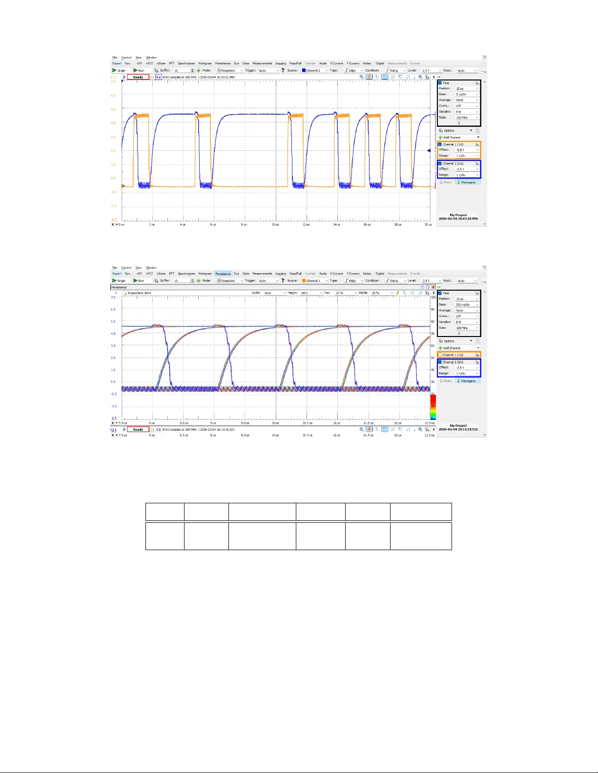
1 A Lo w Cost Discrete Digital Isolator Circuit. Thomas Conway Abstract —This work pr esents a fully discr ete, low-cost digital isolator requiring no specialized ICs and implemented entirely with general-purpose transistors and a two-lay er PCB-embedded air-core transformer . The design avoids vendor lock-in and long-term component obsolescence risks, while pro viding >1 kV isolation, 200 ns propagation delay , and validated NRZ data rates of 1 Mbps. A modified dual-oscillator architecture enables inherent hardware lockout suitable f or half-bridge gate-driver applications. Measured performance and PCB lay out guidelines are provided. Index T erms —Galvanic Isolation, PCB Air Core T ransformer , Discrete Circuit Implementation. I . G A L V A N I C D I G I TA L I S O L AT I O N Galvanic isolation for digital signals is a widespread re- quirement and has been well served for a long time with opto- isolators and more recently integrated micro transformer and capacitiv e coupled commercial IC’ s [1],[2],[3]. Howe ver , for some applications such as lo w volume pro- duction or long lifetime products, a discrete solution using generic components may be desirable. In these cases, a v endor specific IC or specialist process might lead to long lead times or issues with obsolescence. This issue of obsolescence or part discontinuation has been of concern for a long time in the electronics area [4],[5]. There is a need therefore in some applications for a discrete digital isolation implementation that uses widely av ailable components that have multiple sources and are likely to continue in production. Discrete general purpose transistors are one such example and the de vices employed in this design hav e been in production for more that 40 years! I I . D I S C R E T E C I R C U I T I M P L E M E N TA T I O N The circuit described here provides the digital isolation function and consists of a simple, fast startup, discrete LC high frequency oscillator using an air core inductor , that is magnetically coupled to an identical air core inductor on the isolated side and the induced voltage, is rectified to provide a binary digital output. The novelty of the circuit is the simplicity of the design and the use of ubiquitous general purpose transistors with the transformer (i.e. coupled inductors) simply implemented as PCB trace spiral coils on both sides of a standard PCB[8]. The circuit simplicity allo ws the secondary and primary circuits to be implemented using surface mounted components on each respectiv e PCB side without the need for any vias. W ith 1.6mm thick FR4 PCB as used in this design, and the dielectric strength in excess of 20 kV/mm, the breakdown voltages well into the several kV range is easily achiev ed. Thomas Conway is an Associate Professor in the ECE dept. of the Univ ersity of Limerick, Limerick, Ireland Contact: Dr. Thomas Conway Lecturer , ECE Dept Uni versity of Limerick National T echnology Park Limerick, Ireland. T el +353 61 202628, Email thomas.conway@ul.ie Thus high voltage isolation is delivered through the PCB material itself without the need for any high voltage compo- nents or concerns over creep distance specifications[7][9]. A. T ransmitter Side Fig. 1 sho ws the circuit schematic de veloped. The oscillator is the well kno wn cross coupled MOSFET pair which deliv ers a negati ve resistance between the two drain terminals. An LC resonant circuit is normally connected across these two drain terminals, but in this case only an L (inductor) is used, with the parasitic capacitance of the drain source and gate source of the 2N7002 transistors (Q5,Q6) providing the resonance capacitance C. T wo drain resistors (R12,R9) provide the required operating current. The circuit is driven by a 5V logic signal and simply powers the oscillator to transmit a logic 1 or leaves it un-powered, i.e. off for a logic 0. When powered-on, a high frequency oscillation excites the recei ver circuit. This is simply on-off keying in modulation terminology . Prototyping the transmitter circuit indicates a maximum reliable oscillation frequency around 30 MHz with a minimum inductance of 0.4 uH. Choosing a frequency of 15 MHz allows for mar gin in the design and reliable oscillation based on bench measurements with an inductance of 1.6uH. This lev el of inductance is readily achiev able with air core PCB coils of manageable size[8]. Breaking symmetry between the resistors R12, R9 results in a f aster startup of the oscillator and in fact one of the resistors can be completely omitted. B. Receiver Side The isolated receiv er side is based on the identical inductor L2 which is coupled to L1. General purpose NPN transistors (MMBT3904s) Q7 and Q8 in conjunction with R17 and R18 effecti vely implement full wav e rectification and amplification of the induced voltage across L2. T o see this, just consider Q7, L2 and R18 and R17, ignore Q8 which will be turned of f. W ith a positiv e v oltage induced (of more than 2 × V B E ) in L2 (taking its ’ dotted’ side more positiv e) and divided by the potential divider formed by R18 and R17, Q7 turns on, pulling its collector low and outputting a logic 0 at the output (Node D Y). R18 limits the base current into Q7 and the loading added onto the transmitter oscillator . On the opposite polarity of the high frequency c ycle, Q8 (with R17, R18) performs identically pulling the collector of Q4 lo w . During the zero crossings, the output does not go high due to the fact that the transistors Q7 and Q8 are bipolars and subject to saturation when turned on. The slo w recov ery from saturation (typ. 100ns for MMBT3904 at 1mA) effecti vely implements a low pass filter function for the rectified signal and results in a stable logic signal at node D Y . 2 4K7 0V 5V Coupled L1/L2 HV Isolation 5V 0V TRANSMITTER RECEIVER not needed R16 DI DX DY Q8 MMBT3904 Q7 MMBT3904 R17 R18 560 560 560 R9 R12 Q5 Q6 L2 2N7002 2N7002 L1 Fig. 1. Schematic of Digital Isolator using Discrete Components I I I . P C B I M P L E M E N T AT I O N W I T H C O P P E R T R AC E T R A N S F O R M E R Using PCB traces for the coil windings and placing the transmitter part on opposite sides of the PCB provides for a con venient implementation [8]. Using SO T23 devices, i.e. the 2N7002 and MMBT3904 for the transistors with 2010 sized resistors allo ws for the PCB layout sho wn in Fig. 2. An 8 pin DIP packaged IC is also in the picture as a reference scale. (NO TE: The 2N7000 equiv alent SMD device 2N7002 ( < 200mA) should be used and not higher current, lo wer Ron variants as they will not operate satisfactorily with the inductors shown here.) Fig. 2. Layout of transmitter (top side) and receiver (bottom side) for 2 layer PCB The coil is formed with 8 turns of an almost square coil of 200um wide track and 200um track spacing. The length of the inner coil track is 9.7mm on each side. A 2 layer 1.6mm thick FR4 PCB with 35um copper thickness was used for the prototypes. The o verall coil area is about 16mm by 16mm. On the transmitter side, the two 2N7002 devices are placed inside the coil and 2010 SMD pads R9 and R12 are used to bridge across the coil to av oid the need for vias (R12 is actually not needed as mentioned before). R10 and R11 are short circuits (or 0R resistors) with R10 taking the 0V line into the circuit and R11 taking the outside of the coil back into the central circuit. The bottom side coil is identical to the top side coil and directly underneath it to maximize coil magnetic coupling. The resistors R18 and R17 are 1206 size and together with SO T23 transistors Q8 and Q7, fit inside the coil interior . Again bridging resistor pads of 2010 can be 0R resistors to connect across the coil without vias. The pull-up resistor R16 is then outside the coil and can be part of the circuit being driv en in the application. I V . P RO TO T Y P E M E A S U R E D P E R F O R M A N C E The measured performance of the circuit of Fig. 1 imple- mented with the PCB layout of Fig. 2 is sho wn in Fig. 3. The orange trace (DX in Fig. 1) is the input 0/5V digital signal from a 1 Mbps NRZ data source. The blue trace shows the output (node D Y) which is the secondary side data (in verted). A logic propagation delay of around 200ns is seen which should be satisfactory for a range of general purpose applications such as isolated U AR T , or SPI interfaces. Fig. 4 sho ws the corresponding eye diagram which is a good visual representation of the digital transmission ability of the circuit readily supporting a 1 Mbps data transfer rate. The o verall characteristics of the discrete digital ioslator circuit presented in this paper are summarized in table I. V . L O W A N D H I G H S I D E S I G NA L L I N G F O R H A L F B R I D G E D R I V E R One of the motiv ating applications for the circuit develop- ment is for signalling to the high and lo w side driv ers for a half 3 Fig. 3. Measured logic transfer for the prototype PCBs with a 1 Mbps NRZ random data signal Fig. 4. Corresponding Eye Diagram for 1 Mbps NRZ random data T ABLE I O V E RA L L I S O L A T OR C H AR AC T E R IS T I C S V oltage PCB Area Power Propagation Data Rate Est Cost Isolation Dissipation Delay Rate (incl PCB area) > 1kV 3.4 cm 2 TX 25mW (max) 200ns > 1 Mbps 50 ¢ RX 5mW (max) bridge power electronics circuit. When using opto-couplers for this application, it is common to connect the two LEDs in anti- parallel, so that applying a positive voltage turns one on with the other rev erse biased, and a negativ e v oltage turns on the other LED, but both LEDs cannot be simultaneously on, thus providing an inherent hardware lockout to pre vent both the high and low side driv ers simultaneously conducting. Analogous to this, the circuit of Fig 5 employs two digital isolators but combines the two transmitter oscillators into a single circuit, one ’on top’ of the other . W ith the transistor polarities as shown and a 5V logic operation, consider A a logic 0 and B a logic 1, then the v oltage labelled V T X will be +5V and Q12 and Q13 will simply conduct through their internal source-drain diodes supplying power to the oscillator consisting of Q14,Q15, L1 and R21 and coupling the oscillating current of L1 into the coupled coil L2 and pulling the lo w side dri ver signal DLS low (to an activ e lo w power driv er). W ith A a logic 1 and B a logic 0, then V T X will be -5V and Q14 and Q15 will conduct through their internal source- drain diodes supplying po wer to the oscillator consisting of Q12,Q13, L3 and R21 and coupling these oscillating current of L3 into the coupled coil L4 and pulling the lo w side driv er signal DHS low (to an activ e low power driver). W ith A and B both logic 1 or both logic 0, then V T X = 0 and the circuit is un-po wered and neither dri ver acti vated. 4 Coupled L1/L2 HV Isolation TRANSMITTER 4K7 560 560 MMBT3904 MMBT3904 Q5 Q6 R6 High Side RX R5 R8 Coupled L3/L4 4K7 560 560 MMBT3904 MMBT3904 Q3 Q4 R4 R3 R9 Low Side RX DHS HS5V HS0V LS5V LS0V DLS A B L1 L3 L2 560 L4 2N7002 2N7002 2N7002 2N7002 R21 Q14 Q15 Q12 Q13 V TX Fig. 5. High/Low Side Isolation for Half Bridge Application Thus the circuit prev ents both driv ers being activ ated together and is suitable for the half bridge power electronics circuit configuration. Fig. 6 sho ws the measured output for the circuit of Fig 5 implemented on a PCB with similar layouts to those in Fig 2. The measurement shows clean logic wav eforms with a natural dead time of about 300ns (noting that the signals are activ e low). This level of performance is suitable for modest switching frequency power electronics employing IGBT half bridge applications. V I . C O N C L U S I O N S This article has described a simple discrete circuit digital isolator using commonly a v ailable components that achie ves isolation through the use of a PCB transformer with coils on opposite sides of the board and relying on the FR4 board material for the voltage isolation. Such a circuit can easily provide digital data rates of 1 Mbps or can be useful for isolated signalling for power electronics applications such as the high side/low side half bridge power circuit. The ke y attrib ute of the design is the use of ubiquitous general purpose transistors and no special purpose vendor specific parts, thus allowing for a design that supports long life products in critcial applications where single supplier or vendor specific solutions and potential problems with obsoles- cence are of concern. R E F E R E N C E S [1] Broadcom. Optoisolation and Optical Sensor Products. A vailable at: https://docs.broadcom.com/doc/A V00-0254EN [[accessed 21 Mar 2026]. [2] Analog Devices. ADuM361N: 3.0 kV rms 6-Channel Digital Isolator . Rev . D, accessed 21 Mar 2026. A vailable at: https://www .analog.com/en/products/adum361n.html. [3] T exas Instruments. ISO73xx Series Capacitiv e Digital Isolators. TI Dig- ital Isolator Design Guide (Application Note SLLA284). A vailable at: https://www .ti.com/lit/an/slla284g/slla284g.pdf [accessed 21 Mar 2026]. [4] R. Solomon, P . A. Sandborn and M. G. Pecht, "Electronic part life cycle concepts and obsolescence forecasting," in IEEE Transactions on Components and Packaging T echnologies, vol. 23, no. 4, pp. 707-717, Dec. 2000, doi: 10.1109/6144.888857. [5] S. Karaani, M. Zolghadri, M. Besbes, C. Baron, M. Barkallah and M. Haddar, "Systematic Analysis of the Links Between Ob- solescence–Shortage and Reliability–Maintainability–A vailability ," in IEEE Access, vol. 13, pp. 88371-88389, 2025, doi: 10.1109/A C- CESS.2025.3570107. [6] I. Boccato, R. La Rosa, I. Nikiforidis, P . D. Mitcheson, N. Aiello and C. Florian, "A Low-Profile GaN-Based Multi-MHz DC-DC Con verter with an Air-Core PCB Transformer ," 2025 Energy Con version Congress & Expo Europe (ECCE Europe), Birmingham, United Kingdom, 2025, pp. 1-6, doi: 10.1109/ECCE-Europe62795.2025.11238890. [7] J. Sabate, E. Delgado and M. Harfman-T odorovic, "Gate Driver Power Supply for Medium V oltage SiC Mosfets with Air Core Transformer ," 2022 IEEE Energy Con version Congress and Exposition (ECCE), Detroit, MI, USA, 2022, pp. 1-6, doi: 10.1109/ECCE50734.2022.9948213. [8] S. C. T ang, S. Y . Hui and H. S. . -H. Chung, "Characterization of coreless printed circuit board (PCB) transformers," in IEEE Transactions on Power Electronics, vol. 15, no. 6, pp. 1275-1282, Nov . 2000, doi: 10.1109/63.892842. [9] SLUP421 – “Demystifying Clearance and Creepage Dis- tance for High-V oltage End Equipment” A vailable at: https://www .ti.com/lit/pdf/SLUP421 [accessed 21 Mar 2026]. 5 Fig. 6. High side, low side measured output with a 50 kHz ± 5V square wa ve input Thomas Conway received the B.Eng. degree in electronic engineering and the Ph.D. de gree in detec- tion methods for magnetic recording channels from the Univ ersity of Limerick, Ireland, in 1991 and 1996, respectively . He joined Hewlett Packard CPB, Bristol, in 1991 and w orked for two years on the design and de vel- opment of tape drives for computer storage. From 1996 to 1998, he worked as a senior design engineer with Analog Devi ces B.V . Limerick, Ireland and Adaptec Inc., Longmont, CO, USA on disk drive read channels and controllers. He joined the ECE dept at the University of Limerick as a Lecturer in 1999 and lead the Limerick team in the European project on two dimension optical data storage, TWODOS, which was lead by Philips Electronics, NL with teams from TU Eindhoven, NL and Lancaster , UK. He was a Science Foundation Ireland funded inv estigator in the mid 2000s, successfully supervising 3 PhDs each going on to work with industry across Europe. He also started and ran a private consultancy business AL TCWY , providing consultancy to a range of companies both within Ireland and internationally . In the 2010s, he turned his research to a life long interest in electric vehicles and sustainable ener gy . He has published extensiv ely including 14 IEEE T ransactions journals of which he is the primary author on 9, as well as being a named in ventor on 9 patents.
Original Paper
Loading high-quality paper...
Comments & Academic Discussion
Loading comments...
Leave a Comment