A Boost Converter Design with Low Output Ripple Based on Harmonics Feedback
Conventional boost converters are essential to connect low-voltage energy source such as battery with high voltage DC bus in Electric Vehicles due to its simple construction and high conversion efficiency. However, large output capacitor banks must b…
Authors: Haifeng Wang
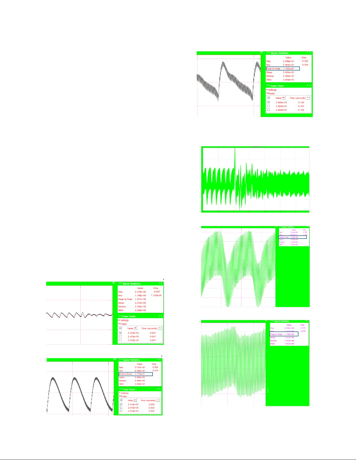
A Boost Con verter Design w ith Low Output Ripple Based on Harmonic s Feedback Haifeng Wang * , Member, IEEE Penn State Univ ersity New Kensington, PA, US * hzw87@ psu.edu Abstract - C onventional boost converters are essential to connect low - vol tage energy source such as batte ry with high v olta ge D C bus in Electric Vehi cles due to its si mple constructi on and hi gh conver sion effi ciency. H owever, larg e output cap acitor banks mus t be used in orde r to reduce t he outp ut vo ltag e rippl es whe n an inv erter i s connec ted to a bo ost converter. In a typica l series hy brid electric vehi cle powertrain, signifi cant voltage and current pertur bati ons wi ll impa ct on batte ry sy stem p erforma nce a nd res ult i n co nsid erable po wer l oss . To address this i ssue, this pa per proposes a ne w control strategy for ripple reduc tion i n the dc - l ink of power electronic converters . In the propos ed met hod, an obs erver i s des igned to adaptiv ely esti mate the dc - link volt age an d current harm onics . The ha rmoni c terms are mult ipl ied by optimi zed ga ins t o control the conv erter’s duty cycle by negative f eedback law. Entire control model for t he p ropose d converte r is illust rate d and robust ness i s veri fi ed. Simul ati on and expe riments show that original volt age and cur rent ri pple magni tude can be reduced significa ntly . Keywords: power electroni cs, observer, feedbac k control 1. Introductio n Elect ric Veh icles such as pu re EV a nd hybrid EV are attractiv e to provide en vironmentally frien dly transpo rtation with rene wable energy. Fi g .1 shows the electrical sy stem configuration in EVs, inclu ding pow er DC - DC con vert er, i nver ter, mo tor a nd bat ter y. Fig .1. EV power convers ion a rchit ec ture Most of the E Vs have both high power dc co nvert er and lo w power conve rter . T he first o ne supplies el ectri c m otor an d th e se cond on e is u sed f o r ventila tion, light ening and other de vices [1, 2] . I n electrical vehicle applic ation s, the major load is typically an inve rter fol lowed by a m otor [3, 4] . The pres enc e of rip pl e an d nois e is an imp orta nt co nsid eratio n in DC co nve rter appl ica tio n s [5] . T he noise s have two compo nents. The first happens at the fundamenta l switchi ng freq uency cal led as ripp le. The second nois e occurs at the very high freque ncy ringing that o ccurs dur ing s witchi ng transitions . The ripple and noise leve ls can be sufficient ly high to advers ely affect other devi ces and parts c onnect ed to the convert er if the ripple are l eft unfilt ered. If electric vehicl es are integrated with electrical grid, the charg ing and dischar g ing circuits w ill induce extra ripples in the orde r of twice the gr id freq uency [6, 7] . Ripp les in t he dc - link are undesirable si nce they cause di stortion a nd pow er l oss , an d gen erate unn ecessary t orque r ipple s . The high freq uency curre nt ripples will enter t he electr ic v ehicl e’s bat te ry sy stem to age battery and deteriora te the a nions’ state of e quilibr ium [6, 8 , 9] . To red uce ri pp le s , interlea ved boost conver ter is widely investigated . But it n eeds shif t sever al chann els so that it has more components and weight as w ell as gener ates high er frequ ency r ipples and losses due t o chan nels’ switch [10] . For ty pical ap plic ation s wher e ripple s a re n o t critic al, they can be filter ed by adding addit ional ceram ic capa cito rs to the DC - D C o utput e nd and input end. B ut t he capacitanc e could be too bi g and vary greatly . In this case, a star tu p prob lem coul d aris e. The output fil ter vol u me w ill be incr eased by adding the extra output capa citors to reduce the output ripple s . I n addition, if “L C” filte ring n etw ork is applie d t o filter rip pl e s , the inductance and the frequenc y of network should be sta ggered with the DC - DC freq uency to avoid mutual interfer ence. Moreover experiments indicates that the vo ltage ripple increases w ith the decreas ing of the ind uctance in small inductanc e condition. The refore, ther e is no doubt that sim ple LC filter cannot ens ure the converter to meet the desired rip pl e requi rements . In noise sensitive appl ications, a need for low r ipp le perform ance is more t han the c onv ert er c an pr ovi de on its own. An external proporti onal - integral fil ter is rec ommen ded to be co nne cte d to t he con vert er’s outp ut. T he fir st step is to cho o se a large va lue of inductor . But l arge induc ta nce will r eq uire a lar ge capacit ance and th e r es pons e of th e fi lter c oul d be significantly slowed. Adding a n ultra - lo w - noise lo w - dro pout regulator or LDO to the converter outp ut is another way to ge t low noise and ripp le in converters. B ut the LDO can only handle a lim ited current that i s usually about 1 A and needs requi r ed capa cito r s along with it. For exa mple, a regu la r LDO an d re qui red c om pon ents nee ds 4 6.8 m m 2 P CB boar d spa ce an d the cost is m ore t han $ 5 f or e ach LDO. T hi s paper prop os es a method to reduce DC - LIN K rip pl e for a ty pical tw o - sta ge conver ter inverter drive circuit that consists of a boost conv ert er c ascad ed by a thr ee - pha s e full br idge inverter and a motor, as depi cte d in Fig. 2. Co mpared with the pre vious wor k [11] , the new ly pro pos ed 7 th orde r au ton om ous LTI control sy stem is applie d to a batter y po wered mo to r drive system . This paper applie s thi s observer based meth od to reduce in ducto r cu rren t harm onics besi des DC - LINK vo ltage ri pples . Moreov er, th e vo lta g e and current harmonic s frequ ency in t he ob ser ver ca n be adapti vely up da ted accord ing to the r eal - time sp eed o f the motor . This p aper al so co mp are s th e r educ ed ri pp l e magnitude with circuit analy sis to prove the effecti veness of the m ethod. Fig .2. Circ uit topol ogy f or a BLDC motor dr iver powere d by a boos t conver ter . 2. Feedback Contr ol design for robus t referenc e tracking and ripple r eduction 2.1 Extractin g rippl e harmon ics v ia an observer Suppo se the above boost converter - inver te r cir c uit is a linear - time - in vari ant (L T I) sy stem repres ented b y its state. I f the sy stem is observable, its state s such as voltag e and cur rent can b e re con str ucted or eva luat ed by an obs erv er. In what fo llows, the se ction expla in s how the dc - link harmoni cs are related t o t he sta te o f the LTI system. T hen t he constructio n of observer follows from st andard p rocedur e [11] . At steady stat e, the dc - link voltage can be expre ssed as ( ) = + cos ( + ) (11) W her e is t he aver ag e of , and are t he magnitude and p hase for the n - th o rder harmonic . β (measur ed in radians) is the frequency of the dc - link rip pl e and is adaptively ad justed based o n motor speed ra tio . T he fir st t hr ee harm onics w ill be s ufficient and they can be used to signi ficantly reduce th e ri pple. So the pape r consider s only the fir st thr ee harmonics. Then ( ) = + cos ( + ) + cos (2 + ) + cos (3 + ) (1 2) DC - LINK volta ge and in duct or cu rrent are t he out put of a 7 th order a utonomous LTI system. Define S = 0 0 0 0 0 0 0 0 0 0 0 0 0 0 0 0 0 0 0 0 0 0 0 0 0 0 0 0 0 0 0 0 0 0 0 0 0 0 0 0 0 0 0 (13) G = [ 1 1 0 1 0 1 0 ] (14) And den ote th e st ate of th e L TI sy stem as x R , then let’s analy ze the vol ta ge first: = , = , ( 0 ) = (15) The t w o des cri ptions (1) an d ( 2) a re rel ated vi a the following eq uations: v = x ( t ) , x = v (16) cos ( + ) = x ( t ) , x x = b cos b sin (17) cos ( 2 + ) = x ( t ) , x x = b cos b sin (18) cos ( 3 + ) = x ( t ) , x x = b cos b sin (19) This m eans t hat each h armoni c can be recon st ru cte d by two of the state v ariables. S ince th e pair (S,G ) is obs erva ble , all its states can be recon st ru cte d from its o utput , which can be eas ily meas ured by AD conv erters . It fol lows that, th e averag e of , all its ha rmonics a nd their derivatives can be ext ract ed fr om via a n obser ver in table 1 . Based on the techno lo gy dealing with unwanted periodi cal signals [2, 12] , the feedback cont rol w ill be constr ucted using no t only the har monics w hich are repr es ented by x 2 , x 4 and x 6 , but als o their der ivatives, x 3 , x 5 and x 7 . Table 1 Funda me ntal a nd ha r monic s fo r the D C volta ge. Funda me ntal Com po nent First Order Harmon ic b cos First Order Harmon ic Der ivativ e b sin Second Order Ha rmonic b cos Secon d O rder Har moni c Der ivativ e b sin Thir d Or der Har monic b cos Thir d Or der Har monic Der ivativ e b sin 2.2 Estim ation of the h armonic s v ia observer Let the state of the obs erver be z a nd the inp ut be : z = ( S LG ) z + L ( 20 ) Let the observer error be e = z x , and e = ( S LG ) e . T his im plies th at the observe r erro r will go to 0 as t tends t o infin ity if S − LG is stab le. L is the observe r gain. Due t o measurement error s, noise, high - frequenc y switching r ipple, the gai n L should be kept within reas onable rang e for accep tabl e conv ergen ce ra te and av oid ove r ampl ify ing nois es . When t he estim ation error e i s suff iciently sm all, the obs erv er state z is be ver y clos e to state x o f t h e LT I system . The harmonics of and thei r deriv atives can be extract ed from the state z. Then state z can be used for d u ty c yc l e feedback control. 2.3 Using t he es timate d harmo nics for feedback Suppo se that the c urrent i L of the inductor L dc i s repr es ented b y a volta ge acros s a resi stor . Le t th e desir ed dc - lin k v oltage be . A s im ple feed back to achie ve robust tracking is D = D + k ( i i ) + k + ( 21 ) W here D is th e duty cycle for th e low side MOSFET of the half - bridge for the dc - dc con vert er and D 0 is a n ominal duty cy cle. i L0 is the nominal inductor current. To red uce dc - link voltage r ipple, an extr a term Kz is added in the abo ve feedba ck co ntrol: D = D + k ( i i ) + k + + ( 22 ) 2.4 The d iscreti zed obser ver a nd dig ital implement ation T he LTI system needs to be discretized for implementatio n in a d igital pr ocessor . Let t he sampling time be T and the discretized state is x [ k ] = x ( kT ) . T he discretized LTI syste m is [ ] = [ ] , [ + 1 ] = [ ] , [ 0 ] = ( 23 ) W here = = 1 0 0 0 0 0 0 0 cos T sin T 0 0 0 0 0 sin T cos T 0 0 0 0 0 0 0 cos T sin T 0 0 0 0 0 sin T cos T 0 0 0 0 0 0 0 cos T sin T 0 0 0 0 0 sin T cos T (24) Sim ilarly , t he state observer is constructed as [ ] = [ ] + ( [ ] [ ] ) ( 25 ) Wher e L d is c ho sen so the eige nval ue s of S L G are withi n t he uni t d isk to keep stable. A simple rule is to choos e the desired eigenvalues wit hin t he unit dis k but v ery c lose t o those of S , which a re a ll o n the unit disk. Let the e ige nva lues of S be , i = 1,2, . . ,7. the eigenvalues of S L G at , i = 1,2, . . ,7. wi t h 0 < < 1 . If the sampling time is v ery small, then shoul d be very close to 1, f or exam ple, great er th an 0.99. Notice that S is 7 b y 7 ma tr i x . T his may s l o w do wn the co mputation in a digital signal p rocess . T o reduce computation time, the system is decomposed i nto o ne fi rst - order sy stem and 3 second order sys tems . 2.5 Sys tem simul ation and Key performa nce eva luation The p rop ose d con tr ol sy stem block diagram is shown i n Fig.3. E ach block in Fig. 3 is ex panded in Fig. 4 for det ails . Fig .3. Bl o ck diagra m for t he ent ire co nt rol sy stem Fig .4. Expanded bl ock di agra m of l ow harm onics boost conve rter - inver ter m otor cont rol m odel The nom inal operating c ondition w as chosen at V s =12V, and V dc =28 V. This re quires the duty cycle for the dc - dc boo st conv ert er to be D 0 = 0.42. And the inductor current for L dc be i L0 =0.9A. The fe edback control was found to be D = D 0. 08 ( i i ) 0. 06 + ( 26 ) w here v is the referen ce val ue for the dc link voltage v . The coeff icien ts were caref ully d esigne d based on a good transient per formance and re asonable steady sta te behavi or. For exam p le, if the coef fici ent for i L − i L0 is l arge, th e duty cy c le will be noisy since the inductor curre nt has large high - frequenc y switching ripple. If this c oefficient is red uced, there w ill be larger overshoo ts in inductor current and v dc . T he co effi cien t for v dc − v ref should be kept small due to t he constraint on the duty cycle and the noises. Increasing the gain f or the integr ator may increas e the overshoots and the ripple siz e. And the duty cycle D is constr ained w ithin [0, 0.8] via a saturat ion function as D must less than 1. For digital im plementation, the paper firs t constr ucted a di scret ized obser ver to e xtr ac t the firs t orde r, the s eco nd - ord er harmoni cs and third - ord er as well as their deriv atives from the state of a 7 th order LTI system. S ince t he r eal r ipple freq uenc y i s 400Hz , = × 400 = 2512ra d /s . With sam pling frequen cy of 18 kHz , the sam p ling peri od i s T = 5. 56 × 10 s . A nd the S is ex pressed as below : S = 1 0 0 0 0 0 0 0 0. 9903 0. 1392 0 0 0 0 0 0. 1392 0. 9903 0 0 0 0 0 0 0 0. 9610 0. 2756 0 0 0 0 0 0. 2756 0. 9610 0 0 0 0 0 0 0 0. 9123 0. 4066 0 0 0 0 0 0. 4066 0. 9123 (27) The desired eigenval ues for S d − L d G ar e ob tained by scaling the eige nvalues of S d with 0.99 [11] . U sing pole placem ent algo rithm, L d i s computed as L = 0. 0098 0. 0195 0. 0019 0. 0192 0. 0037 0. 0189 0. 0047 (28) A s the Fig. 5 shows, t he dc - link voltage is decom posed i nt o a dc com ponent an d harmoni cs by the built observer . Recall that th e first - order and seco nd order harmoni cs corresp ond to z 2 , z 4 and z 6 of the obse rver. z 3 , z 5 a nd z 7 are similar to z 2 , z 4 a nd z 6 but with some ph ase sh ift . Let’s com pare the origin al v dc signal and reco nstructed signals from obser ver states. Fig. 6 (a) shows the ori ginal v dc ( top , bl ue cur v e) a nd t he rec o nstr uc ted v dc (middle, red curve) . Th e estim ati on error i s also plotted as the bl ack curv e at t h e b ot tom of the figur e. The compari son show s the effectiv eness of the obs erver and t hat the 7 th - order model is sufficient for the dc - link voltage. A close up view of the comparison is shown in Fig. 6 (b) . I t is obvious that the curve for the origi nal v dc is fuzzy and thick, due to the high fre quency switchi ng ripple. In c ontrast, the r econstruc ted v dc is clean an d ripple f ree , indic ating that t he high freq uency switching rip ple has been filte red out du e t o effect of the obse rver. Sinc e the fo u rt h - order harmonic is negligible at steady stat e, t he syst e m only need feedbac k the stat e z 2 , z 3 , z 4 , z 5 , z 6 and z 7 to cal culate the duty cycles . A stat e feedba ck is designed b y ad din g two m ore te rm s to as : D = D 0. 08 ( i i ) 0. 06 + 0.3z + 0.2z 0.1z + 0.2z 0. 03 z + 0. 14 z (29) Fig .5. Estimated the d c - link volta ge and its harmonic s (a) (b ) Fig .6. (a ) reconstructed dc - link vo ltage, the original , and the err or; ( b) C lose - up vi ew of recons truct ed dc - link volta ge i n red an d the original in blue The las t tw o coefficien ts are obtained th rough trial and err or. Firs t, th e term for z 3 is set t o 0. By using one di me n sional sea rch an d sim ulation, it is found that t he rip pl e i s minimum when the coefficient of z 2 wa s - 0. 25 . Another one d imensio nal search with the coeff icient of z 2 fixed at - 0. 25 prod uced a value of − 0. 4 for z 3 . T hen other c oeffici ents are dete rm ined in th e sam e way . It should be noted that both terms for z 2 and z 3 are neede d to m inimize ripple si ze. If t he t erm for z 3 i s dis carde d, th e mi nim al rippl e size in creas es. This means that the deriva tive of the first order harmonic also helps to r educe the rippl e size. The same appli es to other har monics. In order to eliminate the output volta ge overshoot and vibra tion at the beginning b ecause o f the observer feedba ck, a delay elemen t i s add ed to the obs erver feedb ack loop with 0.1s. To obser ve the e ffect mo re obvi ous ly , m ore loa d is con n ect ed to t h e m otor . T he load torq ue change increas es the DC - link vo ltage and the voltage ripp les. To reduce th e voltag e rip ple, observe r based control begin to work at 0.1 second. Simulin k is used to con duct t he simu lation of the pro pose d contr ol sy stem. Th e sampl ing ra te can be chosen as 18 kHz . We use 24V DC as the output voltage of boost co nverter to drive 24 V BLDC m otor used i n an experim ent . T he dc - link vo ltage ge nerat ed by th e boos t c onv ert er c ont roll ed by t wo differe nt co ntro l ler s is plotted in Fig . 7 . Fi g.7 (a) sh o w s the volt ag e ri pple redu cti on by switc hing to the har monics feedba ck contr ol ler . The voltage ripple peak to peak value i s quic kly reduced 53 % from 0.37 V s hown in Fig. 7 (b) to 0.17 V sho wn in Fig.7 (c). The response in Fig. 6 clearly shows the reductio n in r ipp le si ze a fter the harm o nic te rm s are fe d back to the du ty cy cle co ntro l ler a fte r t > 0.1 s. Similar to volt age ripple reduction principl e, 3 - order harmoni cs are used in negat ive feed back w ith proper gain to red uce the inp u t curre nt rippl e. T he new ob server feedback gain i s gained by one dimensio nal search a nd si mulation. Curre nt ripple observer based cont rol ler be gin s to work at 0. 2 second. T he inductor current under the mod ified controll er is plotted in Fig.8. T he induc tor curre nt ri pp le reducti on is sho wn in Fig.8 (a). The ripp le peak to peak value i s reduce d 3 0 % fr o m 1.7 A sho wn in Fig. 8 (b ) to 1.2 A sho wn in Fig. 8 (c) . (a) The vol tage r ippl e r educt ion (b) T he or ig ina l vo ltag e r ipp le clo se - up view (c) The red uced voltag e rip ple c los e - up view Fig. 7 . Dc - link voltage rippl e is reduced from 0.37 V to 0 .17V . (a) Ind ucto r cu rrent ripple reduction (b) The origina l current ripp le close - up view (c) The reduced current rip ple close - up view Fig . 8. Indu ctor current ripple peak t o pea k val ue reduce d from 1.688A to 1.156 A To compare the reduced ripple magnitud e in simu lation with ci r cuit an aly sis results , the v o ltage ripple an d cur rent ripp le a re cal culated in next sec tion s. 2.6 Output Volta ge Rip ple Anal ysis To calcu late a mini mum output capac it ance , t he desir ed output vo ltage rippl e percenta ge is set to 1 % of the ra ted output voltage [1 0] . B ased o n Table 2, the o utput capaci tor values for the desired output volta ge rip pl e i s as b elo w : ( min ) = ( ) = . . . = 0. 000337 = 3 37 (7) So a 470 capacitor i s determined to be the output ca pacitor in the tes t. The ES R of the output capa cit or add s mor e rip pl e s. So the total voltage ri pple is given with the equat ion: ( ) = + = 0. 67 (8) Table 2 Compon ents in the sim ulati on model C out (min) =3 37 minimu m output capacita nce Iout (max)= 2. 65 A maxim um output cu rrent D = 0.55 du t y c ycl e fs = 18 kH z minim um switc hing fr eque ncy ΔV out =0.24 V desir ed outpu t voltage ri pple with _ ESR) = 0. 67 With additional out put volta ge ripp le d ue t o capac ito rs ES R ESR = 0.1o hm equ iva lent s eri es resi st anc e of the out put capa citor l =1. 28 A induc tor ripp le curren t V in = 13.9 V typic al input voltage Vout =24 V desi red outpu t voltage L = 0.0 0033 H select ed induc tor valu e 2.7 Input Current Ripple Analy sis The resistance of a CM OS s witch in the closed positi on, re ferre d to as t he on - resistance or R ON , chan ges de pe ndin g on the inp ut volta ge. T his beha vior is usua ll y undesirab le and can signi ficantly disto rt the input signal in some applic ations. A good esti mation for th e in duct or ripple curren t is 20% to 40% of the outp ut cur re nt. = ( 0.2 0.4 ) = (0.9 1.8 ) (9) To calculate the maxi mum switch curr ent is to determine the inductor ripple cu rrent. = = . . . = 1. 28 (10) In sum, the voltage rip ple plotted in simulation is 0 .17 v ( or 0.7% of output DC v oltage) is better than the acc eptable volt age rippl e 0. 67 v calcul ated by a bove circuit analysis. In addition , in ductor curr ent ri ppl e of t he mode l is 1.1 6A (or 43 % of output current) i s also bett er than maximum sw itch current 1.28 A from the a bove circuit analysis. I n a research about t he interleaved boost con verter, t he voltage ripple varies from 0. 3% to 0.43% of outp ut DC vol ta ge when output pow er changes from 20 kw to 70 kw and t he inductor current ripp le var ies from 50 % to 30 % of maximum input curre nt when output power ch anges from 50 kw to 1 70 k w [1 3]. T heir ripple to DC signal ratios, in comparison, are clos e to our resu lts alt h ough the two converter s ’ circuit s and outp ut p owe r a re different. 3. Experiment al Ve rification The experiment circu it in an electric vehicle prototy pe includes DSP con trol ler, boost con ve rter - invert er , b attery and charger, mo t o r d rive r and m otor s sho wn in F ig.9 . Fig . 9 . The electric vehicle prototype in test The detailed experiment parameters are shown in table 3 and table 4. Table 3 BLD C motor parameters Numbe r o f p hase s 3 Back EM F wav eform Trap ezoid al Sta tor phas e resi stan c e (ohm ) 0.41 Sta tor phas e indu ctan c e (H) 0.0007 To rque co nsta nt (N .M/A - peak) 1.4 Back EM F flat area (degrees ) 120 Ine rtia ( J(kg.m^2) ) 9.6 e-5 viscou s d amping ( F(N.m.s) ) 1e -3 pol e pair s 4 Table 4. ALM 12V7s EverSa fe™ b attery: lithiu m - ion batteries Ele ctrical Char acte ristics at 25°C 12V7s EverSaf e™ b att ery Nomin al Volta ge 13.2 V Nom inal Ca pacity 5 Ah Max. Charge Voltage 16 V Reco mmen ded Float Volt age 13.6 - 14.4 V Unde r - v olta ge Limit ( mi n) 8 V Cons tant Power Disc ha rge End Voltage 10V Pro duct Mode l AL M 12V7s, Si ngle U nit W hen motor runs at 100 0 rpm, the co nverter o utput 24 V vo lta ge to power the invert er and drive the motor. Experimental data sh ow th at the boost c onver ter output vol tage ripp le ca n be r ed uced by half. Fig.10 sh ows the volta ge ripple r eductio n by using the har monics feedb ack contro l. T he volta ge ripple peak to pe ak valu e is q uic kly r educed 46% from 0.67 V shown in Fig. 10 (a) to 0 .36 V shown in Fig.10 (b). T his red uc t ion r ati o is approxim ately e qual to the rati o of th e sim ulation exper iment, as demonstr ated in Fig. 6 . (a) (b) Fig. 10 . Conv ert er outpu t volt age ripp le in c lo se - up view : ( a) voltage harmo nics is not fed back to the duty c ycle controller ; (b ) voltage h armoni cs is f ed back to the duty cycle cont ro ller The pr oposed de sign ca n also be used to reduce inductor current rippl e in the b oos t conver ter . T he second te st uses a 0.1 ohm re sistor connec ted in seri es with a n inducto r t o meas ure th e current fl owi ng thro ugh the inductor. Fi g.1 1 plots the curr ent rippl e reduc tion by using the ha rmoni cs feedbac k control. The voltage ripple p eak to peak value is qui ckly reduc ed 22% fro m 306 m v without ha rmo n i cs te r m feedba ck cont rol in Fi g.1 1 (a) to 239 mv w ith the pro pose d h armoni cs f eedback control in F ig.11 (b ) . This rat io of ripple redu ct ion is clo se to the ra tio of the simulatio n exper iment, a s demons trated i n Fig. 7. (a) (b) Fig .11 . Ind uc to r current ripp le sampling wave for m in c lo se - up view: The sys tem d oes n ot u se har moni cs fee db ack in (a); the sy ste m u s es har moni cs fee dback c ontr ol in (b ) 4. Conclusi on The pap er address ed con verter rip ple reduct ion problems for a power system drive n by battery or other DC power so urce s . A cont rol stra teg y for re ducti on of the dc - link ri pple i s propo sed fo r a two st age boo st invert er. The m ain i dea i s t o use an observer to extract the har monics o f the dc - link vo ltage and curr ent to u s e the har monics for feedback contr ol of the dc - dc boo st converter. The mot or's speed i s sam pled and us ed to ada ptive ly ad jus t the freq ue ncy o f the har moni cs i n the observer. The effect iveness of the co ntrol design methods was validat ed by both simul ation an d expe ri ment s . T he results de velo ped in this p aper will find pos sibl e applic ation s in elect ric, hy brid and plug - in hybrid electric vehicles , wind systems and photovoltaic s ystems. Si nce the rip ple red uction i s achieved by f eedback control of observer stat es, the method can be applied to re duce other fix ed frequency ripples b esides voltag e and current ripp les . REFERENCES [1] A. N ahavand i, M. T . Hagh, M . B. B. Sharif ian, and S. Dan yali, " A Nonis olated Multi inp ut Mu ltiout put DC - DC B oost Conv erter for Elec tr ic Vehic le Ap pli cati on s," (in Engl ish) , Ie ee Tr ansactio n s on P owe r El ectro nics, vol. 30 , no. 4, pp . 1818 - 1835 , Apr 2015. [2] H. Jung , H. F . Wang, and T . S. Hu, "Cont rol design for robus t trackin g and smoot h tran sition in power systems wit h bat ter y /supe rca pac itor hy bri d en er gy sto rage devic es," (i n English ), Journa l of Power Sourc es, vol. 267, pp . 566 - 575, Dec 1 2014 . [3] W. C heng sh uai, J. Che n, X . C henf e ng , and L. Z h iyang , "A daptive con trol stra teg y o f a f uel cel l/batte ry h ybr id pow er sy stem," in 2 016 A merica n Co ntro l C onfe rence (ACC), 2016 , pp. 7492 - 7497. [4] D. Zhao , E. W inw ard, Z . Ya ng, R. S tobart, and T. Stef fe n, "De coupl ing contro l o f e le ctrifie d tur bocharged diese l engine s," in 20 16 A merica n Co ntrol Co nfe re nce (ACC), 2016 , pp. 4207 - 4212. [5] M. Ras hed, C . K lumpn er , an d G . A she r, " Hig h Per for mance Mul tilev el Conv er ter Topo lo gy for Inte rf acing E ner gy S tora ge Sy stems with Medi um Voltage Grids, " (in Engl ish), I econ 2010 - 36th Annual Con feren ce on Ieee Indu str ia l Elec tron ics Soc iet y, 2010. [6] K. U ddin, A . D. Mo ore , A. Bar ai, and J . Marco , "T he effec ts of hi gh f requen c y curr ent ri pp le on elect ri c ve hicle battery perfor mance ," A pplied Ene rgy , vol. 178, no. Supplement C, pp. 142 - 154, 2 016/09/1 5/ 2 016. [7] Q. C. Zh ong an d G . C. K onstanto po ulo s, " No nline ar current - limitin g contr ol for grid - tie d inv erter s," in 2 016 America n Contr ol Conferen ce (ACC), 2016 , pp. 7472 - 7477. [8] H. F . Wang , M. Tah an, a nd T . S. H u, " Effects of rest time o n e quiv ale nt circ uit mode l fo r a L i - ion batte ry ," (in En glish), 2 016 America n Cont rol Conferenc e (Acc), pp. 3 101 - 3106 , 2016. [9] L . Devar akonda, H. F . Wang , and T . S . Hu, " Parame ter identif ica tio n of circu it m ode ls f or l ead - acid batte ri es unde r no n - zero in it ial condi tions ," (in Engli sh), 201 4 America n Contr ol Conferen ce (Acc), pp. 4360 - 4365, 2014. [10] H. Q. Wen an d B. Su , "Hyb rid - mod e int erlea ved b oost con vert er des ign for f uel c ell elec tr ic v ehi cles ," (i n Engl ish) , E ne rgy Co nve rsio n and Mana gemen t, vol. 122, pp . 477 - 487, Aug 15 2016. [11] F. F assinou, H. F . Wang , L . Dev arakond a, and T . S . Hu, "Obs erver - based me tho d fo r re duction o f d c - link vol tage rippl e in two - stage boost inverters ," (in Engli sh), 201 4 American Control Confer enc e (Ac c), pp. 4 348 - 4353 , 2014. [12] T. S. H u, A . R. T eel , and Z . L . Lin, "L yapunov charac terizatio n of for ced o scil latio ns," (in E nglis h), Automat ica, vol. 41, n o. 1 0, pp. 1723 - 1735 , Oct 2005 . [13] H W en , and B S u , “P ractic al I mple mentatio n of an Inter lea ve d B oost Con vert er for Elect ri c Veh icl e Applic ation s”, Journa l of Power El ectron ics , vol. 4, no. 4, Jul 201 5.
Original Paper
Loading high-quality paper...
Comments & Academic Discussion
Loading comments...
Leave a Comment