Theory and design of a phase-inverted balanced coupled-line DC-blocker
A planar DC-blocker suitable for differential mode signaling applications is designed and fabricated. The theory of this component is explained in a new form which utilizes the wave scattering transfer matrix. The proposed interpretation of the trans…
Authors: J. H. Lee, S. K. Park, M. Y. Kim
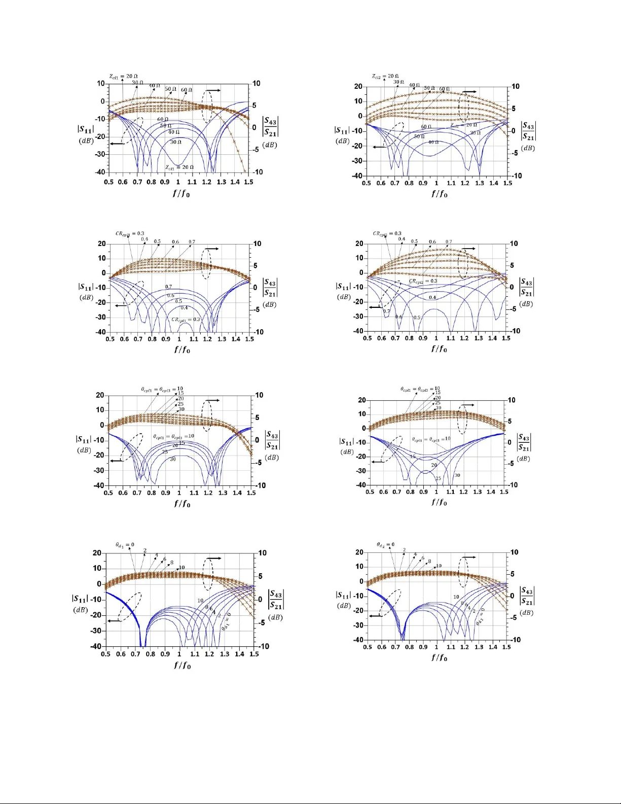
This paper is a preprint of a paper submitted to IET Microwaves, Antennas and Propagation . If accepted, the c opy of record will be available at the IET Digital Library > REPLACE THIS LINE WITH YOUR PAPER IDENTIFICATION N UMBER (DOUBLE-CLICK HERE TO ED IT) < 1 (a) (b) Fig. 2. Difficulties in a double-conductor to triple-con ductor balun transition design: a) abrupt truncation o f the shielding b) electrical connection of the shielding to the global ground. Abstract — A planar DC-blocker suitable for differential mode signaling applications is designed and fabricate d. The theory of this component is explained in a new form which utilizes the wave scattering transfer matr ix. The pr oposed interpretation of the transfer matrix is most suitable for series (cascade) elements like DC-blockers. In addition to the theoretical enhancement, design of a compressed balanced DC -blocker inserted through a shielded broadside coupled stripline (SBCSL) transmission line is presented. The return loss of better than 10 dB is obtained at 50- ohm differential-mode input ports of the fabricated DC -blocker in the entire frequency range of 5.6-8. 4 GHz. The lowest air-gap width in the presented structure is about 10 times bigger than that of a conventional coupled-line structure. So, the structure is much less sensitive to fabrication tolerances. Mor eover, the DC- blocker is likely to tolerate higher DC -voltage differences. Also, a demonstration for a millimeter-wave version of this DC-blocker suitable for integrate d circuits (ICs) ap plications is proposed for future development . The final achievement of this paper is design and fabrication of a wideband substrate integrated waveguide ( SIW )-mediated balun structure for single-ended measurement of a balanced SBCSL component. The fabricated balun exhibits a nearly perfect coaxial-mode to coupled-st ripline differential- mode conversi on in the full range of 5-9 G Hz. The presented balun is successfully utilized to derive the scattering parameters (S -parameters) of the fabricated balanced SBCSL DC-blocker. Index Terms — coupled-line structures, SBCSL, SIW, DC - blocker, differential mode transmission line, balu n. I. I NTRODUCTION HEORY of planar multi-conductor transmission lines (TLs) and coupled-line circuit elements are well established for the decades [1]-[3]. So far, various realizations for filters, directional couplers, baluns, etc. based on coupled-line elements have been proposed [4]. The serie s DC -blocking is a task well suited for coupled-line structures since the structure is wideband due to the intrinsic travelli ng wave effect of coupled lines. [4]. Beside the coupled-line realization, there exist other DC-blocking solutions: like discrete lum ped capacitors for printed circuit boards (PCBs) and metal finger capacitors or metal-insulator-m etal (MIM) capacitors for ICs [5]-[7]. At low frequencies, the lumped capacitors are used This work is under the support of Iran National Science Fo undation (INSF). Mostafa Abdolhamidi is with S chool of ECE, University of Tehran, Tehran, Iran. (email: abdolhamidi@ut.ac.ir) Mahmoud Moh ammad-Taheri is with School of ECE, University of Tehran, Tehran, Iran. (email: mtaheri@ut.ac.ir) due to their small size. Howeve r, at higher frequencies the coupled-line DC-blockers exhibit lower losses, thus they are preferable [4]. In addit ion, for applications like trans former coupling of cascaded IC circuit stages [ 8] – [9], one can modify coupled-line DC-blockers in order to provide extra functionalities such as phase inversion, impedance matching and so on. Successful demonstration of transformer coupled active ICs for millimeter-wave applications can be found in the recent papers [1 0]- [1 3]. In this sense, a modified phase- inverted DC -blocker can be approximately seen as a unit-ratio transformer which can be utilized as an interface of two cascaded active stages with the same characteristic impedances (Fig. 1) . Previously, theory of design and operation of conventional coupled- lin e DC-blockers have been explained in terms of even and odd modes characteristic impedances [2], [4]. In this paper, using the TL capacitance and inductance matrices, we present an alternative derivation based on the wave scattering transfer matrices. This derivation is mostly fit for cascaded circuits where the wave scattering transfer matrix of the whole circuit is simply obtained by successive multiplication of wave scattering transfer matrices of all stages. The derivation of overall wave scattering transfer matrix of a multi-step DC- blocker is covered in section II . In addition, by the presented mathematical analysis, we show that the operational bandwidth of the DC -blocking stage will automatically Theory and Design of a Phase - Inverted Balanced Coupled - Line DC - Blocker Mostafa Abdolhamidi and Mahmoud Mohammad-Taheri T Fig. 1. Equivalence of a phase inverted DC -blocker to a 1:1 transformer. > REPLACE THIS LINE WITH YOUR PAPER IDENTIFICATION N UMBER (DOUBLE-CLICK HERE TO ED IT) < 2 broaden by implem enting the DC -blocking function in side a balanced TL. In the next section, we present a phase-inverted DC -blocker for SBCSL structure . Since aspect ratios (AR) of the m etallic tracks in a PCB are normally very low [14], obtaining high values of couplings between adjacent metallic traces i n a PCB is a difficult task and generally results in extremely close coupled traces . Our propose d design is a single-layer PCB structure in 5-10 GHz frequency range in which the loose coupling problem is properly so lved by use of auxiliary couplings bet ween metallic trace s. The last remarkable contribution of this work is the design of a novel coaxial line- to -SBCSL wideband balun which we use as an interface for the measurement of the DC -blocker S- parameters. In our proposed balun, we have used a SIW-based interface to solve the problems which usually appear in the connection of a shielded balanced TL to an unbalanced TL. These problems are namely the undesired radiation (single- frequency or wideband) (Fig. 2a), and the excitation of unwanted resonant modes within the balun structure (Fig. 2 b) . The former appea rs if the conductor shielding is truncated, while the latter is normally a consequence of short-end termination of the conductor shielding. In addition, the mentioned SI W interface f acilitates the correction of balun phase and amplitude imbalance. This problem exists in balun transitions which have been designed based on lumped element [ 14 ]- [17] or coupled-line Marc hand balun dividers [1 8]- [20] . Al so, our propos ed balun does not require high values of e ven to odd mode impedances ratio which is necessary in the solution proposed by [2 1]. The design procedure of the explained balun is also discussed in section I II . The fabrication and measurem ent processes are presented in section I V. In section V we show that the fabricated microwave PCB phase-invert ed DC-blocker can be redesigned for millim eter wave IC applications. A simulation of a tightly compressed spiral-form DC -blocker in millimeter wave is presented as a future w ork in this section. II. T HEORY I MPROVEMENT A. Wave Scattering Transfer Mat rix Representation Fig. 3a shows a pair of typical common-ground coupl ed traces. The depicted structure if is seen as a four -port network like that of Fig. 3b can be represented by a wave scatterin g transfer matrix ( ), using the procedure rigorously explained in Appendix. The input and output power waves are related to each other throu gh by: (1) According to the derivation given in Appendix, is equivalent to an exponential matrix of the form: (2) where is the coupled-line electrical length and is an involutory matrix (that means ) defined by (a) (b) (c) Fig. 3. Use of a pair of co mm on -ground coupled tracks as a fo ur-port network: a) arrangement of the coupled pair, b) its f our-port equivalent network, c) two-port network which is to be used as the basis of the DC - isolated transition. (a) (b) Fig. 4. Variations of as a functio n of frequency for different values of and CR: a) conto urs, b) contours. > REPLACE THIS LINE WITH YOUR PAPER IDENTIFICATION N UMBER (DOUBLE-CLICK HERE TO ED IT) < 3 (a) (b) Fig. 6. Simple equiv alent circuit of the proposed DC-blocker: a) ci rcuit schematic diagram, b) differential mode and co mmon mode excitations. (A12) and (A15) in Appendix, respectively. Now, suppos e we left ports (2) and (3) of Fig. 3b open to derive an expression for a wave scattering transfer matrix for a two-port network of Fig. 3c which is a si mple circuit model for a one-stage DC- blocker. After some m athematical manipulation one can find that : (3) where (4) In (4), ( )s are the elements of the ) 4 4 ( matrix . According to (4), and (A12), (A15) and (A20) given in Appendix, depends on the op erating frequency ( , coupled-line section length ( ), electromagnetic (EM) wave velocity ( ), the reference impedance ( ), and the capacitance per unit length matrix of the coupled-line structure ( ). The advantage of us ing wave scattering transfer m atrix as propo sed above ov er conventional impedance matrix notations used in classic references [1], [3] is its compatibili ty with cascaded circuit architecture. For instance, overall ) 4 4 ( wave scattering transfer matrix for a multi-step (n- step) DC-blocker, is equal to: (5) or (6) which can be simply writ ten as (7) Then, the wave scattering transfer matrix of the n-step DC- blocker is simply calculated using (4). It is obvious that all other network parameters (like Z-parameters or S-paramet ers) can be directly calculated f ro m the derived . No other network representation, namely the conventional Z - parameters representation has a simple form of (7) for cascaded circuit architecture wh en the port number is greater than 2. B. Bandwidth Improvement in B alanced Architecture In this subsection it will be shown that for a balanced TL architecture, the performance of a coupled-line DC-blocker is better than that of other DC-isolation solutions. This is due to this fact that its frequency response is automatically improved when is used inside a balanced configuration. The scattering parameters of the two-port DC-blocker ( of Fig. 3c can be simply derived from . It is clear from (A20) in Appendix that, regardless of the configuratio n of the coupled-line cross section, the imaginary part of vanishes if (8) This condition is identical to and . Thus, our DC-blocker should be designed to work between two of these transmission nulls. For more convenience we set . Using (4), we can plot the frequency response of for different values of and in the frequency range of , where and are the coupling ratio and coupled-line characteristic impedance, respectively and defined by (A21) and (A22) of Appendix . Fig. 4a shows the CR=0.5 contours in the plane for different values of ; and Fig. 4b shows the contours for different values of CR. (a) (b) (c) Fig. 5. Effect o f differential mode excitation on the reference i mpedance of a two -port network: a) i mpedance representation of the structure of Fig. 3c, b) series connection of two networks with diff erential excitations, c) equivalent single-ended circuits of part (b). > REPLACE THIS LINE WITH YOUR PAPER IDENTIFICATION N UMBER (DOUBLE-CLICK HERE TO ED IT) < 4 (a) (b) (c) (d) (e) (f) (g) (h) Fig. 7. Scattering para meters of the DC-blocker equivalent circuit of Fig. 6a fo r different design parameters values, port numbering is def ined in Fig. 6b: scattering parameters as f unctions of: a) , b) , c) co upling ratio ( ), d ) coupling ratio ( ), e) electrical length ( ), f ) electrical length ( ), g) electrical length ( ), h) electrical leng th ( ). > REPLACE THIS LINE WITH YOUR PAPER IDENTIFICATION N UMBER (DOUBLE-CLICK HERE TO ED IT) < 5 These two figures illustrate that for a fixed CR, lower values of show better frequency response in terms of the return losses. In addition, for a fixed , better return losses in a wider frequency band are obtained for higher values of CR . We know that higher values of CR are achieved by narrowing the dielectric gap between coupled-line conductor traces which, as explained befo re, introduces some pract ical problems. On the other hand, increasing (to decrease ) is identical to using very thin conductor traces which is not a practic al strategy. So, it will be desired to decrease the reference impedance value ( ). If the circuit of Fig. 3c is used as a two port network, it can be described by its impedance parameters (see Fig. 5a ). A series arrangement of two networks like that of Fig. 5a is shown in Fig. 5b. According to the illustrated vo ltage and current signs in Fig. 5b, the excitations of two series networks have opposite signs. Because of this differential excitation, we can convert each excitation port to a series connection of two -ohm ports and set the voltage of their connecting node to the zero. So, the circuit is equivalent to Fig. 5c where it is shown that the scattering parameters at -ohm ports of the network of Fig. 5b are identical to those at -ohm ports in Fig. 5c. Thus, the differential mode excitatio n it self halves the reference impedance value. So, if we design two quadrature wavelength coupled-line structures and insert them in (+) and (-) paths of a differential-mode transmission line, we can achieve a wideband DC-blocker without any need for tightening the dielectric gap between two adjacent conductor traces or decreasing the thicknesses of the conductor traces. III. D ESIGNS AND SIMULATIO NS A. DC -blocker The simplest equivalent circuit for our proposed SBCSL DC -blocker is shown in Fig. 6a. It consists of two separ ate similar paths of open-ended cascaded coupled-li ne sections ( s ) each connects an input SBCSL conductor trace to an output SBCSL trace. It is seen in the figure that each path comprised of a cascaded connection of five separate four-port networks, where the first, thir d and last networks (namely cpl1, cpl 2 and cpl3 ) are coupled-line sections and delay1 and delay2 are isolated delay lines. Since the figure implies that cpl3 and delay2 are rotated copies of cpl1 and delay1, respectively, their corresponding scattering transfer matrices are equal to: (9) (10) where ( 11 ) So, scattering transfer matrix of the cascaded coupled- line sections is derived as (1 2) In (12 ) and are calculated by (2) and is simply equivalent to (1 3) where and are the electrical lengths of the depicted delay lines . The differential mode and common mode equivalent circuits of the DC -blocker are shown in Fig. 6b. It is seen in the figure that in the differential mode, the DC-blocker is approximately equivalent to the series connection of two networks and a phase-inverter block . can be derived from using the same procedure that we calculated from (look (3) and (4)). Also Fig. 6b illustrate s that in the common m ode, the DC-blocker is approximately equivalent to the parallel connection of two networks. According to (A20) - (A23) cpl1, cpl2 and cpl3 sections are characterized by their electrical lengths ( s) , coupling ratios (CRs), matched impedance of the coupled-line sections ( s) and the reference impedance ( ). As we later show, the depicted delay lines are added to the structure only for practical issues and they are assumed m atched to in our primary design. The scattering parameters of the circuit of Fig. 6a as a function of different circuit param eters are plotted in Figs. 7a- 7h. The scattering parameters are calculated at port1, port2 of the differential m ode circuit and port3 and port4 of the common mode circuit as depicted in Fig. 6b . In eac h figure, two groups of curves are plotted which are namely (i n differential mode) and which shows the selectivity of the DC -blocker between the differential mode and common mode signals (or approxim ately the common mode rejection ratio CMRR) . All curves have been plotted as a function of normalized frequency ( ) . is the frequency that the electrical leng th of the coupled-line sections is equal to . It is seen from the figures that one can achieve about 66 % of relative bandwidth for a differential mode input return loss of better than 15 dB and better than 5 dB. Figs. 7a, 7b imply that there is a tradeoff between bandwidth and level for different values of and . This tradeoff is seen in Figs. 7c, 7d for different and values, too. Figs. 7e, 7f show that the electrical lengths of the coupled-line sections (when their total electrical length is equal to ) only affect the input return loss of the DC-blocker. Finally, it is seen in Figs. 7g, 7h that both the bandwidth and bandwidth are shortened when the elect rical lengths of the delay lines ( and ) increase. > REPLACE THIS LINE WITH YOUR PAPER IDENTIFICATION N UMBER (DOUBLE-CLICK HERE TO ED IT) < 6 (a) (b) (c) Fig. 8. Single-layer PCB realization o f the DC -blocker of Fig. 6a: a) and un optimized realization of Table. I, b) ou r propo sed optimized design, c) scattering p arameters of th e optimized desig n for values listed in Table. II. TABLE I U NOPTIMIZED DESIGN VALU ES FOR THE COUPLED - LINE SECTION OF F IG . 8 A (length) TABLE II D ESIRED VALUES FOR TH E D C - BLOCKER OF F IG . 8 B . (a) (b) (c) (d) Fig. 9. Optimized DC -blocker: a) single-layer PC B realization of the component for SBCSL structure , b) input and output SBCSL structu res cross section s, c) detailed specifications of the transition, d) scatte ring parameters based on the ports defin ition of Fig. 6b. Now, we consider the case of an unoptimized DC -blocker with design parameters listed in Table. I. According to Fig. 7a such a DC-blocker shows a wideband be havior around the center frequenc y of (about 66% of relative bandwidth with return losses of better than 15 dB). The cross section of a typical realization of cpl1 and cpl2 with specifications replaced by values in Table I for a single-layer PCB is shown in Fig. 8a. In contrast to the IC realization which is practically feasible, the PCB realization has some limitations due to the quasi-TEM wave propagation which does not have any analytical solution. The even and odd modes of a single-layer PCB coupled-line structure have different effec tive permittivities and so experience different phase velocities. Since, there is no analytical expression for the even and odd modes impedances with res pect to the dimensions of the coupled-line structure, these im pedances should be empirically calculated like those of [ 22 ]. As shown in Fig. 8a, the metallic traces should be very close to each other (0.03 mm). This tight > REPLACE THIS LINE WITH YOUR PAPER IDENTIFICATION N UMBER (DOUBLE-CLICK HERE TO ED IT) < 7 TABLE III V ARIATION OF THE NORMALIZED CENTER FREQUENCY ( ) AS A FUNCTION OF PERTURBATIONS IN THE WIDTH AND LENGTH OF THE DC - BLOCKER 1.07 1.06 1.05 1.04 1.04 1.02 1 1 1 0.98 0.97 0.96 0.98 0.96 0.94 0.93 TABLE IV V ARIATION OF THE NORMALIZED 10 - DB RETURN LOSS BANDWID TH ( ) AS A FUNCTION OF PERT URBATIONS IN THE WIDTH AND LENGT H OF THE DC - BLOCKER 1 1.04 1.09 1.125 0.94 1 1.05 1.09 0.82 0.92 1 1.05 0.74 0.83 0.92 1 spacing of metallic traces is not practically realizable. Even if one can realize this narrow gap, there is a high risk of dielectric breakdown in the case of unequal DC voltages of the traces. Also, the unnecessary 1. 1- mm tra ces widths and low 0.7-mm distances from top and bottom shielding are the other disadvantages of this realization. To avoid the mentioned restrictions, we have designed our DC -blocker in the form illustrated in Fig. 8b. This figure shows a half of the DC-blocker which is a path between the input SBCSL (+) trace and the output SBCSL ( -) trace following Fig. 6a definitions. The other half has the same but rotated structure. The figure shows that and are top- layer and bottom-layer edge-coupled coupl ed-line structures, respectively. But, is a top-bottom broadside-coupled coupled-line structure w hich allo ws the coupling ratio ( ) to be increased to the desired value. In addition, consists of two separate delay sections: a top- layer trace ( ), and a connection of a metalliz ed via and a bottom - layer trace ( ). It is obvious from the figure that this configuration already features the phase inversion property. The design values of the optimized DC-blocker with the configuration of Fig. 8b is listed in Table. II. These values are obtained for the best return loss and common mode rejection performance. It is worth mentioning that a big restriction in our design is the values of and which for the sake of feasibility and fabrication limitations cannot be decreased very much. W e remember from Fig. 7g, 7h that these two parameters seriously affect the design bandwidth. However, Table. II shows that the total electrical length of the proposed DC -blocker is approximately 80 deg which is 10 deg smaller than that of a simple quadrature-length structure. Fig. 8c shows the scattering parameters of the optimized design. It is shown that better than 10 dB of return loss is obtained in a 50% of relative bandwidth. Also the common mode rejection level is better than 5 dB in t he same frequency band. The optimiz ed DC-blocker configuration is simulated in Ansoft HFSS (Fig. 9a). It is connected to the input and output SBCSL structures at both sides. The final structure is finely tuned in Ansoft HFSS for the best possible performance. The shown metalized vias complete the outer metalli c shield inside the Tac onic-30mil-RF35 laminate. The cross section of the input/output SBCSLs (as illustrated in Fig. 9b) are composed of two broadside-coupled 2.2- mm 70 - copper traces spaced 2.5 mm from the top and bottom aluminum shields. In this structure for differential mode propagation. The thorough depiction of the structure in Fig. 9 c (co mpare to the model of Fig. 8b) shows that there is a 0.35- mm airgap between the coupled traces. This is a no ticeable modification to the mentioned 0.03- mm . The traces have 0. 7 mm widths and spaced from the auxiliary grounds. Fig. 9c shows that the top and bottom layers are symmetric but mirrored with respect to each other. The shown 1- mm ground vias and 0.7- mm traces vias are both easy to fabricate. There is not any airgap smaller than in the shown structure. The connecting SBCSL conductor traces of 2.2- mm width are also shown in the figure. The simulated S -parameters of the transition at the input and output 50 -ohm SBCSL ports are shown in Fig. 9d. Assuming the parameters are plotted in the same scale as that of Fig. 8c . The figure implies that the simulate d structure shows frequency responses very close to that of the ideal structure. A return loss of better than 15 dB for a bandwidth of 2.8 GHz (39 %) and 10 dB for a bandwidth of 3.2 GHz ( 45 %) have been achieved. Also, the common mode rejection level is better than 4 dB in the same 50 % of relative bandwidth. The overall length of the transition is 5 mm which is equal to at 7.2 GHz. This length includes the required interconnects and add itional airgaps between the open-end coupled- lin e sect ions and the input / output SBCSLs. It is worth testing th e sensitivity of the designe d phase- inverted DC -blocke r with respect to dimension changes. Since the DC-blocker has too many dimension parameters, we define a width scale factor ( ) and a length scale factor ( ) and calculate the effect of these two fa ctors on the value of the DC -blocker center frequency ( and 10-dB return loss bandwidth ( ). The original DC-blocker has the center frequency of and 10-dB bandwidth of (5.6-8.8 GHz), as shown in Fig. 9d. Also, the width and length of the original design are and , respectively . We have simulated several DC-blockers with perturbed widths ( ) and lengths ( ) and listed the values of their corresponding normalized center frequency ( and normalized 10-dB return loss bandwidth ( in Table. III and Table. IV, respectively. It can be infered from Table. III that increasing either the DC- blocker width or its length will decrease but with different > REPLACE THIS LINE WITH YOUR PAPER IDENTIFICATION N UMBER (DOUBLE-CLICK HERE TO ED IT) < 8 (a) (b) (c) Fig. 10. P roposed n ovel SIW -mediated balun: a) overall configuration, b ) explosive view of the constitu tive parts, c) dimensions, (a) (b) Fig. 11. HFSS simulatio n of the proposed SIW -mediated balun: a) its scattering parameters, b) balu n common -mode r ejection ratio and other figures of merit. scales. However, as shown in Table. IV increa sing DC-blocker width and length have inverse effects on the 10 -dB return loss bandwidth ( . Wider bandwidths can be achieved by either increasing DC-blocker width or decreasing its length. Also, for a same values of width and length scales rem ains unchanged. Moreover, it is obvious from Table. III and Table. IV that is more sensitive to dimension changes in comparison to . B. SIW -mediated Balun For the measurem ent of the balanced DC-blocker S- parameters, we have designed a wideband SIW-mediated balun. This com ponent is expected to properly transform the unbalanced coaxial TEM single-ended mode into the balanced SBCSL quasi-TEM different ial mode. The proposed balun configuration is illustrated in Fig. 10 a. It simply consists of a coaxial- to -SIW and SIW- to -SBCSL transitions. The main role of the intermediate SIW section is to electrically connect all SBCSL condu ctors together, namely (+) , (-) and the shielding. The SBCSL structure is com posed of two copper traces printed on the top and bottom layers of a Taconic-RF35-30mil laminate (w ith and =0.0018), while the whole PCB is surrounded by two aluminum lids (F ig. 10 b). The transition contains of two slots on the top and bo ttom layers which gradually transforms the SIW guiding mode into the differential mode of the SBCSL. Since the slots are entirely covered by the aluminum plates air cavities, there will be no chance for any radiation loss mechanism s. Also, du e to the very small height of the cavities, no resonant modes are excited and probable resonances and total power reflections are all entirely eliminated. It is worth to mention that, the top and the bottom copper layers of the PCB have ident ical patterns. The dimensions of the SBCSL transmission line are chosen similar to those of the DC-blocker of Fig. 8b. Also, the dimensions of the SIW ( like ) are chosen in such a way that in the entire frequency range of 5 .6 - 8.8 GHz (which is our desired transit ion band) it operates in its single-mode condition. The detailed dimensions of the transition (PCB and aluminum lids) are found in Fig. 10 c. In this figure it is seen that the transition slots are placed inside top and bottom cavities. The total length of the transition is about 13 mm. The S -paramet ers of the transition between the SIW and the SBCSL ports (highlighted in Fig. 10 b) are plotted in Fig. 11a wh ich is designed and simulated in Ansoft HFSS. As can be seen, from slightly above the SIW cutoff frequency (4.7 GHz) the return loss exceeds 20 dB and remains above this value in the entire SIW single-mode band. The and figures show no signs of radiation losses or total power ref lections or resonant- like behavior. A completely flat response for is achieved > REPLACE THIS LINE WITH YOUR PAPER IDENTIFICATION N UMBER (DOUBLE-CLICK HERE TO ED IT) < 9 Fig. 13. Designed coaxial- to -SIW tran sition and its S- parameters. Fig. 14. Sch ematic of the DC-blocker prepared for the measure ment by means of balun transitions and coax - to -SIW connectors. Fig. 15. Photo of the fabricated sample, asse mbled and de-assembled views. TABLE V COMPARISON BETWEEN THE PROPOSED BALUN PERFORMANCE WITH SOME OTHER FAMILIAR SOL UTIONS PRESENTED IN F IG . 12. Input/output matching Radiation loss solution1 good weak solution2 weak (resonant behavior) good solution3 weak (narrow band) good our work good good Fig. 12. Co m parison of o ur proposed balun performance with other available solutions. above 5 GHz which is definitely novel in the literature. The E- field intensity distribution is plotted in the same figure which shows proper transition of the electromagnetic wave inside the structure. Also, the E-field vector distribution at the symmetry plane shows that the transition has properly excited the propagating differential m ode of the SBCSL structure. The simulation results of the proposed balun when is used a s divider are depicted in Fig. 11b. More than 40 dB of comm on mode rejection ratio (CMRR) is achieved above 5 GHz. Also the phase and am plitude imbalance are both less than 0.5% above 5 GHz. The sim ulations show that the balun has an excellent behavior as a 180-degree divider, too. A br ief comparison is able to clarify the advantage of the presented structure over other coupled -line balun solutions. To compare, we consider three different solutions (Fig. 12): the shielded parallel plate balun with tapered transition stages [23] (solution1), the parallel plate balun with tapered transition stages and truncated shielding (solution2), and the coaxial- to - SBCSL Marchand balun transition (solution3) [24]. These solutions were compared with our design with respect to the level of the undesired radiation and the input/output matchings levels. As listed in Table. V, the first solution suffers from high levels of radiation losses due to the closeness of the shielding to the tapered sections. In the second solution, single-frequency total power reflections at the input and output ports does not allow the balun to have a wideband behavior. Also, solution3 shows a narrow-band behavior when the familiar Marchand balun is used as a one input one output balun transition. As we discussed earlier, in our proposed balun the level of the undesired radiation is very low and the input and output return losses show non-resonant wideband behaviors. IV. F ABRICATION AND M EASUREMENT The scattering parameters of the coax- to -SIW transition of Fig. 10 a is shown in Fig. 13 . The design and optimization of this transition is based on the CPW- to -SIW transition proposed in [ 25 ]. The figure shows that the return loss of better than 28 dB is ob tained for this transition in the frequency range of 5.2 – 8.4 GHz. More to say, shows a smooth and non-radiative behavior in the fr equency region of interest. Next, for the sake of measurement, the designed coaxial- to -SIW transition, SIW- to -SBCSL balun transition and the SBCSL DC-blocker are all attached together in a series and back- to -back fashion as sho wn in Fig. 14. The fabricated circuit is shown in Fig. 15. It consists of a Taconic RF-35 30mil laminate which is patterned on bot h sides. The circuit is assembled on a machined aluminum plate (Bottom plate). Another machine d aluminum plate (lid) is > REPLACE THIS LINE WITH YOUR PAPER IDENTIFICATION N UMBER (DOUBLE-CLICK HERE TO ED IT) < 10 placed on top of the PCB and is firmly attached to the PCB and the bottom plate. Also, the bottom side of the PCB and the total assembled structure are shown in the figure. The top lid and the bottom plate construct the required closed cavities for the SBCSL structure, DC -blocker and the balun transitions. For eac h S-parameters measurement process, the high frequency SMA connectors will be attached to the assembly from sidewalls. We have designed a si mp le microstrip line on the PCB (it can be seen in Fig. 15) to model the dielectric and conductor losses in our simulations. We have used a piecewise linear model for the utilized dielectric to precisely compensate for highe r values of losses seen in our measurem ents. With this modified dielectric model, 0.3 dB of difference is seen between the sim ulated and measured of the microstrip line in the entire 5.6-8.8 GHz frequency band . Fig. 16a shows the fabricated sample of the structure of Fig. 14. The top aluminum lid is removed in Fig. 16a for a better illustration. T he S-paramet ers are m easured at the depicted coaxial ports. The measure d and simulated results are shown in Fig. 16b. It is seen that t he measurem ent and simulation results have simil ar behavior in the entire frequency band. The cu toff frequency and the nulls of are excellently predicted in the simulati ons. Even the upper band frequency responses of both simulation and measurement are approximately similar. Except for a very narrow frequency band around 6.5 GHz, is better than 10 dB in 5.6-8.4 GHz for the simulations and measurements. This means the relative bandwidth is 40% for the center frequency of 7 GHz . Also, the measured insertion loss is less than 1.6 dB in 5.7-8.4 GHz frequency band which its difference with that of simulation is less than 0.4 dB in the entire 5.9-8.4 GHz band. Since both the DC-blocker and the SIW-based balun (a) (b) Fig. 16 . The fabricated DC-blocker with its connecting balun s. A) photo of the structure, b) its S-para meters. (a) (b) Fig. 17. The calibration kit: a) photo of the calibration k it, b) S - parameters of Line circuit. (a) (b) Fig . 18 . S -parameters of the Error box: a) , b) .. > REPLACE THIS LINE WITH YOUR PAPER IDENTIFICATION N UMBER (DOUBLE-CLICK HERE TO ED IT) < 11 transition contribute the results shown in Fig. 16b, we have fabricated an auxiliary calibration kit to separately extract S- parameters of each component. This kit (as shown in Fig. 17a) consists of Line and Through circuits which are almost identical except for the length of the SBCSL connecting section. Before advancing with the calibration, it is worth looking at the S-param eters of the kit itself. Line circuit S- parameters are depicted in Fig. 1 7b. The figure implies a good agreement between the simulations and measurements results. The SIW cutoff frequency and null frequencies of are properly predicted. The measured inserti on loss is less than 1.5 dB in the frequency range of 5.6-8.4 GHz, while in the same band, the measured return loss is better than 10 dB. The difference between and is less than 0.45dB. Now we return to the calibration process. Since the depicted Error boxes of Fig. 17a are identical, the scattering transfer parameters of Through and L ine circuits are ( 14 ) (15) respectively. We derive and from the measurement results of the calibration kit ( and ). Now, if we assume a new m atrix as (1 6) it is evident from (1 6) that the eigenvalues of are the diagonal elements of while is a matrix whose columns are eigenvectors [ 26 ]. Figs. 18a, b illustrate the calculated S-parameters of the Error box ( ). As the cutoff frequency of second guiding mode for the SIW is around 9.4 GHz, above this frequency, the excitation of the SIW second mode invalidates the calibration method. So, the figures are plotted in the frequency region of 4.5-9.5 GHz. It is seen from Fig. 18a, b that the return loss for the fabricated structure is better than 10 dB in the entire fre quency band of 5 -11 GHz and better than 15 dB in 5.2 -9.4 GHz frequency range. The difference between insertion loss of the fabricated error box and that of simulated is less than 0.5 dB in the frequency region of 5.2-9.4 GHz. Corresponding to the increase in to about -15 dB, the insertion loss increases to about 0.8 dB around 6.5 GHz. It seems that the fabrication tolerances (specifically within the tapered slot transition area) are responsible for t his litt le diffe rence between the simulation and measurement results. In the next step, if we call the scattering transfer matrix of the circuit of Fig. 16 a , we can easily find that (17) Since and networks are identical but mirrored, we have (18) where (19) So, the scattering transfer matrix of the transition is calculated as ( 20 ) The corresponding curves ( are depicted in Figs. 19 a, b. The overall behaviors of simulation and measurement S-parameters are similar. As seen, is less than -10 dB in the whole region of 5.6-8.4 GHz (40% of equivalent relative bandwidth). Also, the insertion loss is better than 1. 5 dB in the same frequency band and better than 1 dB in 5.9-8.4 GHz (about 1/3 of relative bandwidth). The difference between of simulated and that of measured is less than 0.5 dB in 5.6-8.4 GH z. The small increase in the difference of the simulated and measured insertion losses are due to the fact that the attenuation constant which is derived from the applied calibration method is extremely sensitive to the precision of the measurement process. So, even very small errors in the TABLE VI C OMPARISON OF OUR PRO POSED DC - BLOCKER WITH SOME OTHER AVAILABLE SOLUTIONS . DC -blocker type Dimensions Smallest feature size 10 dB return loss bandwidth Insertion loss Single -phase fabrication Balanced configuration Phase inversion Quarter-wave coupled-line [23] 110% 0.5 dB yes no no Interdigital capacitor [24] 33% 0.5 dB yes no no ATC 800b capacitor [25] - 100% 0.4 dB no no no This work 35% 1 dB yes yes yes (a) (b) Fig. 19 . S -parameters of the DC-bloc ker: a) , b) . > REPLACE THIS LINE WITH YOUR PAPER IDENTIFICATION N UMBER (DOUBLE-CLICK HERE TO ED IT) < 12 measured values have no ticeable effects on the calculated attenuation constant. Actually, for this error to be significantly suppressed, we need to use several different length Line circuits and implement the procedure presented i n [ 30 ] which is out of the scope of this paper. Summarily, the fabricated DC-blocker presents an acceptable performance in 5.6-8.2 GHz which is approximately a 1/3 octave frequency region. Since according to Fig. 9c, its total length is only 5 mm or approximately @ 7 GHz ( @ 7 GHz for the SBCSL differential mode) this component can be easily used where a compressed phase-inverted differential mode DC -blocker is required. A short comparison of the proposed component to some other DC blocking solutions is presented in Table. VI. It is seen that the ph ase inversion functionality is only present in this work. Also , none of the other solutions have been designed for bala nced TLs. Except for the ATC capacitor, the smallest feature size of our DC-blocker is much bigger than those of other solutions. In terms of the operational bandwidth, the ATC capacit or and the quarter- wave coupled-line have the best performance, but in the expense of cost and requirement of separate mounting phase in the former and very narrow gap size and feature size in the latter. In addition, the overall dimensions of the presented solutions are approximately in a same order of magnitude. Finally, the ATC capacitor has the best performance in terms of its insertion loss. V. F UTURE WORK We can redesign our fabricated microwave DC-blocker for multi hundreds gigahertz IC applications. In this case both the guided wavelength and the circuit dimensions shrink by approximately comparable scales. Figs. 20a, b show the cross section of a coupled-line sect ion suitable for CMOS IC DC- blocker realization, and a typical 50-ohm SBCSL transmission line, respectively . Both structures are realizable in an identical CMOS IC. The differential mode guided wavelength in the depicted SBCSL is around in 300 GHz which is more than on e hundred times greater than the depicted traces widths and thicknesses and inter-trace spaces. So, the millimeter band IC DC-blocker will occupy very large area with respect to the SBCSL cross section and needs to be significantly miniaturized. To decrease the DC-blocker size without degrading its performance, we use the idea of spiral-form coupled structures which has been previously reported by authors [ 31 ], [ 32 ]. First, we stretch the input SBCSL (+) trace in an inward right-hand spiral-form in the upper layer. W e put a metalized via at the spiral end and stretch the trace on the lower metal layer in an outward left-handed spiral-form. We set the total si ze of the open-ended trace at at 300 GH z. This trace forms a coupled-line section if is put near another trace stretched right-handed inward in the lower metal layer and left-handed outward in the upper layer (Fig. 2 0c ). To form the phase inverted balanced DC-blocker it is enough to place a similar spiral-form cou pled-line structure in the input SBCSL (-) trace path, as depicted in Fig. 2 0d . The figure shows that the total length of the millimeter-wave IC DC-blocker is at the center frequency which is similar to our fabricated microwave PCB DC-blocker. W e simulate the structure in Ansoft HFSS and calculate at the shown input SBCSL differential port. The result that is shown in Fig. 20e illustrates that the input return loss is better than 10 dB in a170-420 GHz frequency band. Two more simulation results are also depicted in the figure which belong to DC -blockers comprised of coupled-line sections with and coupling ratios of and , respectively. Although the coupled- line sections of our spiral-form DC-blocker have coupling (a) (b) (c) (d) (e) Fig. 20. The millimeter-wave IC DC-blocker: a) cross section of the SBCSL input TL co m pleter structure, b) cross section of the coupled -line section c) layer- by -layer illustration of th e coupled-spiral sections, d) paths of all four conductor traces of the input and output trans m ission lines, e) mathematical model respo nse and A nsoft HFSS si m ulation results for part (d) > REPLACE THIS LINE WITH YOUR PAPER IDENTIFICATION N UMBER (DOUBLE-CLICK HERE TO ED IT) < 13 ratios of , the overall spiral DC-blocker scattering parameters are sim ilar to those of s sim ple balanced DC- blocker with . It shows that the overall coupling ratio has been increased in our structure by using the proposed spiral configuration. It means that the space between coupled traces can be increased. As a consequence, the tolerance of the DC voltage difference will be sign ificantl y improved. Since more detailed discussi on needs precise measurement results, we leave it hear for a possible future fabrication and measurement processes. VI. C ONCLUSION In this paper we first proposed a wave transfer matrix representation for a coupled-line configuration. We expressed the superiority of this method over other solutions for cascade circuits architecture. Then we theoretically describe that the couple-line structu re is very s uitable for the reali zation of DC -blockers inside balanced transition lines. W e proposed a compact coupled-li ne DC-blocker with built-in phase inversion capability for 5 -10 GHz applications. Also, a very wideband SIW-based coax- to -SBCSL balun transition was proposed which was successfully used for the measurement of the fabricated DC-blocker. Our measurem ent results show that both the DC-blocker and the balun transition can be used for differential signaling applications. In addition, we showed that the coupled-line phase inverted DC-blocker can be properly designed and integrated for millimeter-wave IC applications using a two-step spiral- form configuration. A CKNOWLEDGMENT The authors would like to thank Iran National Scientific Foundation (INSF) for financial supporting this research work. The authors also would like to thank Mr. Ahmadi Ali-Abad of Fara-Afrand co. for his support i n circuits fabrication. A PPENDIX The wave scattering transfer matrix of an infinitesim al length of a coupled-line TEM structure can be simply derived from its relevant equivalent circuit (Fig. A1 a). Based on the figure notations, the voltages and currents have the following relations: (A1) (A2) where (A3) (A4) The input and output power wave vectors can be derived from the corresponding voltages and currents defined at a real reference impedance , as (A5) (A6) We consider the circuit of Fig. A1 a as a four-port network of Fig. A1 b and assign a four- dimensional wave scattering transfer matrix ( ) to it, as (A7) Eq. ( A1 ) to ( A7 ) result in the following relation for (A8) In (A8) represents a ) 4 4 ( identity matrix. ( A8 ) can be simplified since we have assumed a lossless TEM wave transmission along the coupled-line structure. This assumption which is a good primary approximation for the case of PCB and IC transmission line structures has an important outcome: Both the scalar electric potential and l ongitudinal part of the vector ma gnetic potential satisfy Laplace’s equation. It means that if we define a capacitance per unit length matrix ( ) and an inductance per unit length matrix ( ) for the coupled-line structure, these two matrices are related to each other by (a) (b) Fig. A1. The eq uivalent circuit o f an infinitesimal length of a TEM coupled-line structure: (a) LC repr esentation, (b) fo ur-port equivalent network. Fig. A2. The eq uivalent circuit o f an infinitesimal length of a TEM coupled-line structure: (a) LC repr esentation, (b) fo ur-port equivalent network. Fig. A3. A pair of quarter-wavelengt h couple-line as a directional coupler. > REPLACE THIS LINE WITH YOUR PAPER IDENTIFICATION N UMBER (DOUBLE-CLICK HERE TO ED IT) < 14 (A9) where is the velocity of electromagnetic wave propagation along our transmission line. These matrices are related to and by (A10) (A11) where is the total length of the coupled-line section and is the infinitesimal length associated with the coupled-line element of Fig. A1 a. Using ( A9 )-( A11 ) and by defining the electrical length param eter ( ) as (A12) Eq. A8 can be rewritten as: (A13) where (A14) (A15) and matrices contains information of power distribution inside the four-port network. By this definition, the wave scattering transfer matrix of a cascade connection of four-port networks (like that of Fig. A1 b) in the style depicted in Fig. A2 is sim ply equal to: (A16) if the contribution of vanishes and (A17) This shows that the scattering transfer matrix of a coupled-line section can be described in the form of a matrix exponential. Since is an involutory m atrix, we have (A18) This characteristic is useful in Taylor series representation of : (A19) or (A20) We can look at the coupled-line section a s a -matched coupled-line structure (Fig. A3 ). If we suppose that the coupled-line structures are symmetric ( becomes a symmetrical matrix) we ha ve [16]: (A21) (A22) where and are odd and even impeda nces of the coupled-line structure and and are related to by ( A4 ) and (A 10 ) and CR is the coupling ratio of the quarter- wavelength couple-line structure if used as a directional coupler in the configuration of Fig. A3 . By some m athematical manipulation, we obtain: (A23) By this interpretation can been directly expressed in terms of , and using (A20). R EFERENCES [1] George L. Matthaei, Leo Young, E. M. T. Jones, “Microwave filters, impedance matching networks and coupling structures,”, 1st ed . Artech house, 1985, ch. 13. [2] Ra mesh Garg, In d er Bahl, Maurizzio Bozzi, “Microstrip lines and slotlines”, 3 rd ed. Artech house, 2013, ch. 8. [3] D. M. Pozar, “Microwave engin eering,”, 4th ed. John Wile y & sons, 2012, ch. 7. [4] Rajesh Mongia, Inder Bahl, Prakash Bhartia, “RF and microwave coupled-line circui ts,”, 1st ed. Artech House, 19 99, ch. 3 - 13. [5] Q.S.I. Lim, A.V Kordesch, R.A. Keating, "Performance Comparison of MIM Capacitors and Metal Finger Capacitors for Analog and RF Applications", Pr oceedings RF an d Microwave C onference 2004. RFM2004 , pp. 85-89, 5 – 6 Oct 2004. [6] Eun seok Song, Kyoungchoul Koo, Jun So Pak, Joungho Kim, "Through - Silicon- Via -Based Decoupling Capacitor Stacked Chip in 3-DICs", Components Packaging and Manufacturing Techn ology IEEE Transactions on , vol. 3, pp. 1467 -1480, 2013, ISSN 2156- 3950. [7] Kalavath i Subramaniam, Alb ert Victor Kordesch, Mazlina Esa, "Increased Capac itance Density with Metal -Insulator-Metal – Metal Finger Cap acitor (MIM-MFC )", Semiconducto r Electronics 2006. ICSE '06. IEEE International Conference on , pp. 567-571, 2006. [8] Alan W. L. Ng, Howard C. Luong, "A 1-V 17-GHz 5- mW CMOS Quadrature VCO Based on Transformer Coupling", Solid-State Cir cuits IEEE Journal of , vol. 42, pp. 1933 -1941, 2007, ISSN 0018-9200. [9] T. A. Tran, S. Vehring, Y. Ding, A. Hamidian, and G. Bo eck, "Evaluation of transformer an d capacitor coupling in W-band broadband CMOS power amplifiers", Wire less Symposium (IWS), 2016 IEEE MTTS International , March 2016. [ 10 ] M. Vigiliante, P. Reynaert, “ Analysis and design o f an E -band transformer-coupled low-noise quadrature VCO in 2 8- nm CMOS”, IEEE Trans. Microw. Th eory Techn. , vol. 64, no. 4, pp. 11 22-1132, Feb. 2016. [ 11 ] T. LaRo cca, J. -C. Liu, and M.-C. Chang, "60 GHz CMOS A mplifiers Using Transformer-Coupling and Artif icial Dielectric Differential Transmission Line s for Compact Des ign," IEEE Journal of Solid -State Circuits , vol. 44, no. 5, pp. 1425 -1435, May 2009. [ 12 ] A. Vishnipolsky, E. Socher , "A compact power efficient transformer coupled differential W-ban d CMOS amplifier", Proc. IEEE 26-th Conv. Elect. Electron. Eng. Israel , pp. 869 -872 , 2010. > REPLACE THIS LINE WITH YOUR PAPER IDENTIFICATION N UMBER (DOUBLE-CLICK HERE TO ED IT) < 15 [ 13 ] N. Defer m and P. Reynaert, "A 100 GHz transformer -coupled fully differential amplifier in 90 nm CMOS," in Rad io Frequency Integrated Circuits Symposium, RFIC 2010, IEEE, pp. 35 9-362, May 2010. [ 14 ] D. Kuylenstierna, P. Linner, "Desig n of broad -band lumped-element baluns with inherent impedance transformation", Microwave Theory and Techniques IEEE Transactions on , vol. 52, pp. 2739-2745, 2004. [ 15 ] Yu Ye, Ling-Yun Li, Jian-Zhong Gu, Xiao-Wei Sun, "A Bandwidth Improved Broadband Compact Lumped -Element Balun With Tail Inductor", Microwave and Wireless Components Letters IEEE , vol. 23, pp. 415-417, 2013, ISSN 1531 -1309. [ 16 ] F. Zhu, W. Hong, J. X. Chen, K. Wu, "Ultra-wideband single and dual balun based on substrate integrate d coaxial line te chnology", IEEE Trans. Microw. Theory Techn. , vol. 60, no. 10, pp. 3013-3022, Oct. 2012. [ 17 ] K. S. Ang, Y. C. Leong, C. H. Lee , "Analysis and design of miniaturized lumped-distributed impedance-transforming baluns", IEEE Trans. Microw. Theory Tech. , vol. 51, no. 3, pp. 1009 -1017, Mar. 2003. [ 18 ] T. G. Ma, Y. T. Cheng, "A miniaturized multilayered marchand balun using coupled artificial transmission lines", IEEE Microw. Wireless Compon. Lett. , vol. 19, no. 7, pp. 446 -448, Jul. 2009. [ 19 ] H. -X. Xu, G.-M. Wang, X. Chen, T.-P. Li, "Broadband balu n usin g fully artificial fractal-shaped co mposite right/left handed transmission line", IEEE Microw. Wireless Compon. Lett. , vol. 22, no. 1, pp. 16- 18, Jan. 2012. [ 20 ] Chia -Hui Lin, Cheng-Hsun Wu, Guan-Ting Zho u, Tzyh-Ghuang Ma, "General compensati on Method for a Marchand Balun with an arbitrary connecting segment between the bal ance ports", Micro wave Theory and Techniques IEEE Transactions on , vol. 61, pp . 2821 -2830, 2 013, ISSN 0018 -9480. [ 21 ] R. Sturdivant, “Balun d esigns for wireless, mixers, a mplifie rs, and antennas,” Applied Microwave , Vol. 5, summer 1993, pp. 34- 44. [ 22 ] D. M. Pozar, “Microwave engineeri ng,”, 4th ed. John Wiley & sons, 2012, ch. 7, sec. 6, pp. 350, Fig. 7.30. [ 23 ] Rajesh Mongia, Inder Bahl, Prakash Bhartia, “RF and microwave coupled-line circ uits,”, 1st ed. Artech Hou se, 1999, ch. 11, pp. 395 -399. [ 24 ] J. -C. Lu, C.-C. Lin, C.-Y. Chang, "Exact synthesis and i m plementation of new high-order wideband marchand baluns", IEEE Trans. Micr ow. Theory Techn. , vol. 59, no. 1, pp. 80 -86, Jan. 2011. [ 25 ] Taringou , F., Dou sset, D., Borne mann, J., and Wu, K., "Substrate - Integrated Waveg uide Transitions to Planar Trans mission-Line Technologies," IEEE MTT-S International Microwave Symposium Digest, 1-3, 2012. [ 26 ] F. Xu, K. Wu, and W. Hong, “Domain decomposition FDTD algorit hm combined with numerical TL calibration technique and its app lication in parameter extraction of substrate integrated circuits,” IE EE Trans Microw. Theory Tech. , vol. 54, no. 1, pp. 329 – 338, Jan. 2006. [ 27 ] D. Lacombe, and J. cohen, “Octave band microstrip D C blocks,” IEEE Trans, Microwave Theory Tech ., Vol. 22, Aug. 1972, pp. 555- 556. [ 28 ] Inder Bahl, “Lumped elements for RF and microwave circuits,”, 1st ed. Artech House, 2003, ch. 7, pp. 238 - 242. [ 29 ] Inder Bahl, “Lumped elements for RF and microwave circuits,”, 1st ed. Artech House, 2003, ch. 5, pp. 167 - 170. [ 30 ] D. C. DeGroot, J. A. Jargo n, R. B. Marks, "Multiline TRL revealed ", ARFTG Conference Digest Fall 200 2 60th , pp. 131-155, 2002. [ 31 ] M. Ab dolhamidi and M. Moha mmad- Taheri, “A compact wideband differential interconnect f or co mplete series DC-isolati on of integrated circuits above 100 GHz” Proceedings Asian Pacific Microwave Co nf. (APMC) 2016. [ 32 ] M. Abdolh amidi and M. Mohammad - Taheri, “Conta ct -free solution for millimeter-wave on - wafer VNA measurements” Proceedings Iranian Conf. Millimeter-wave THz Technol. (MMWaTT) 2016. [ 33 ] D. M. Pozar, “Microwave engineering,”, 4th ed. John Wiley & sons, 2012, ch. 7, sec. 6, pp. 351 – 355. Mostafa Abdolhamidi was born in Tehran, Iran. He received the B.S. and M.S. degrees in Fields and Waves in Communication engineering from University of Tehran, Iran in 2004 and 2008 respectively, and now is work ing toward Ph.D. in the same field and the same university. From 2008 he has started a close collaboration with Fara-Afrand Co. in Tehran where he has focused on the design and manufacture of different passive and active RF circuits for high power terrestrial video and audio broadcasting applications. During these years the company was successful in the pro duction of the first m ulti-kilowatt national digital video broadcast transmitter system and has continued to the mass production of nationwide high power broadcasting systems and sub-systems. In parallel to the industrial activity, Mr. Abdolhamidi started to work on leading-edge millim eter- wave technology during his Ph.D. where he is designing novel passive interconnects for IC m illimeter-wave applications. Mahmoud Mohammad-Taheri was born in Saryazd, Yazd, Iran. He received the B.Sc. degree in electrical engineering from the Sharif University of Technology, Tehran, Iran, in 1979, and the M.Sc. degree in telecommunication systems and the Ph.D. degree in microwave engineering from the University of Essex, Essex, U.K., in 1986 and 1990, respectively. From 1982 to 1985 and 1990 to 1991, he was with the Telecommunication Research Center as a Microwave Research Engineer and Project Manager. From 1997 to 2001, he was involved with the Oil Ministry of Iran as a consultant in offshore and on shore telecommunication projects. From October 2001 to November 2002, he was on sabbatical leave with the University of Waterloo, where he taught electromagnetic and he was involved with the design and analysis of ultra-wideband distributed amplifiers (DAs). From August 2008 to September 2011, he was a Post-Doctora l Fellow with the University of W aterloo, worked in the area of design and fabrication of millim eter wav e low noise amplifier. Since 1991, he has been a member of the School of Electrical and Computer Engineering, Faculty of Engineering, University of Tehran, Tehran, Iran, where he is currently an Associate Professor. He has authored or co-aut hored over 60 papers in well-known journals and conferences. He has authored four books. His research interests are multimode dielectric-loaded cavity microwave filters, radio wav e propagation, microwave remote sensing, ultra-wideband DAs, and millimeter and sub-m illimeter wave low noise am plifiers.
Original Paper
Loading high-quality paper...
Comments & Academic Discussion
Loading comments...
Leave a Comment