Image Processing with Dipole-Coupled Nanomagnets: Noise Suppression and Edge Enhancement Detection
Hardware based image processing offers speed and convenience not found in software-centric approaches. Here, we show theoretically that a two-dimensional periodic array of dipole-coupled elliptical nanomagnets, delineated on a piezoelectric substrate…
Authors: Md Ahsanul Abeed, Ayan K. Biswas, Md Mamun Al-Rashid
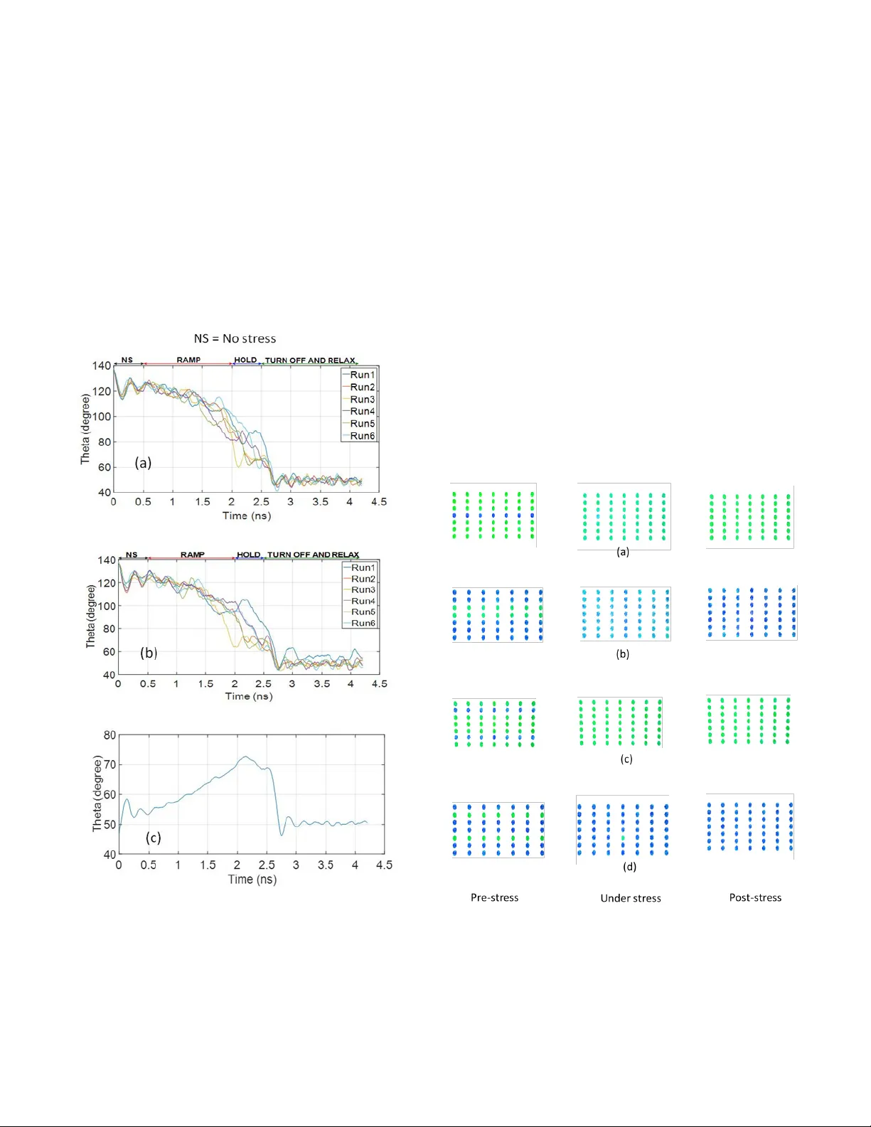
1 Abstract — H ardware based i mage processi ng offers spee d and conve nie nce n ot fo und i n sof twar e - centri c approac hes. Here, we show theoretically that a two - di mensi onal peri odic a rray of dipole - coup led elliptical nan omagnets, delineat ed o n a piezoelect ric subst rate, ca n act as a dynamical sy ste m for speci fic imag e proc essi ng f uncti ons . Eac h nan omag net has tw o st able magnetizati on states t hat enco de pix el color (blac k or whit e). An imag e cont ai ning blac k a nd w hite pix el s is f irst c onv ert ed t o voltage states and then mapped into the magnetization states of a nano mag net arr ay w it h magneto - t un neling j uncti ons (M TJs) . The s a me MTJ s are empl oye d to r ea d out the pr ocess ed pix el colors later. Dipole inte ract ion betw een the nanomagn ets i mpl e me nt s s p eci fic i mage processi ng tasks such as noise reduction and edge e nhance ment detection. These fu nctions a re trig ger ed by a pply ing a g lo bal s trai n to th e nan omag net s wi th a voltage dro pped across t he piezoele ctric subst rate. An i mage cont aini ng an arbitr ary n umbe r of bl ack and w hi te pix el s ca n be processed i n few nanoseconds wi th very low energy cost. Index Terms — Image Processi ng, Micro magnetics Nano magnetic Devic es, S traint roni cs. I. I NTRODUCTION ARDW ARE based image processing can be extremely fast and yet c onsumes l ittle ene rgy. Here, w e propose an d anal yze a magne tic syste m f or t his p urpo se and sho w tha t it can carry out specific image processing tasks in a few nan oseconds w hile con suming m iniscu le amount of en ergy. T he c hoice of nano ma gnet s for i mage p roc essi ng is motivated b y the desire for e nergy efficienc y. Traditional hardware platforms for ima ge processing emplo y field - programmable gate arrays [1] , dio des [2] , nan owir es [3] or quan tum dots [4 ]. The im age processing function is implemented via charge exchange between these elemen ts, whic h al ways r es ults i n c urr ent fl ow a nd as soc iated 2 IR po wer los s. I n co ntras t, no cur rent ha s to p ass t hro ugh This w or k is supp orted in part by the Common wealth of Virgi nia, Center for I nn ovative Techn ology (CIT) via the Comm onwealt h R esear ch Commerci aliza tion Fund (C RCF) Matchin g Funds Program MF - 15 - 006 - MS . M.A.A , A .K.B. and S .B. ar e w ith the D epartme nt of Electr ical and Comp uter E ngine ering , Vir ginia Co mmonw eal th Unive rsity , R ichmond, VA 232 84 USA (e - m ail: abeedma@v cu.ed u, biswasa k@vcu.e du, sband y@vcu.edu ). M.M.A and J.A. a re w ith both th e Dep art ment of Elec tri ca l and Compu ter Engi nee ring and the Dep art ment of M echan ica l and N ucl ear Engi nee ring , Virg inia Com mo nwe alth Univ ers ity, Ric hm o nd, V A 232 84 U SA (e - mail: alrashi dmm@v cu.ed u , jatulas im ha @vcu. edu) nano magne ts in a n i mage p ro cessing funct io n, whi ch eliminates the 2 IR loss i n the devi ce. F urther mor e, the interaction between nanomagnets is “wireless” (no physical wires) and is mediated by dipole interaction. Hence there is no ener gy los s in i nte rco nnect s ei ther , whic h fur ther i mpr oves t he energy efficiency. These con siderations make n anomagnetic systems a very attractive ch oice for image processing. II. T HEORY In thi s paper, we will consi der processi ng of blac k and white images only, i.e. each pix el is either black or whit e. We will encode a pixel’s color – black or white – in a sta ble magnetizatio n orientation of a nano magnet. T his will requir e the nano ma gnet to have only two stabl e mag netiza ti on orientations. T he simple st way to achie ve that is to choo se nanomagnets that are s haped like an elliptical disk . A static fixe d m agnetic field is directed along the minor axis of the ellipse as shown i n Fig. 1(a). That will ensure that the nano magne t’s magnet iza tion will have onl y t wo sta ble orientations in the ellipse ’s plane as sho wn i n Fig. 1 [5 ]. The angle ϕ b etw een th em is a functio n o f the str engt h of t he magnetic field an d the eccentricity of the ell ipse. It can be adjust ed to ~90 0 by tuni ng t he magnetic field stre ngth [5][ 6 ]. Next consider a two - dime nsio nal a rra y of na no magnet s in a global magnetic field directed along the ellipses’ mi nor axes as sho wn i n Fi g. 1( b) . Eac h nano magne t wil l no w exp eri ence a dipole f ield du e to dipole intera ction with its ne ighbors . Thi s fiel d depends , among oth er things, on the nanom agnet’s own magnetizatio n state, as well a s the states of its ne ighb or s. The eff ect of the dipole f ield on any nanomagn et is to m ake on e of the two stable magnetization orientation s preferred over the other. Which on e is pref erred wil l depend on the magnetization stat es of the neighbors. Therefore, the preferred colo r ( black or white) of the p ixel enco ded in a ny nano mag net will be dictat ed by the c olors of the surroun ding pix els. This dependenc y resul ts in s pecifi c image pr ocess ing functi ons. A. Trigge ring the image proce ssing ac tion The image p roc essin g func tio n req uir es a nanomagnet to transition to it s preferred magnetiztion o rientatio n. However , this does not happen auto matically. T he potential ene rgy profil e of an isolate d nanoma gnet has two de gener ate mi nima corresp onding to the two stab le magnetizatio n orientations. When a nano mag net is p lace d in the vici nity o f othe rs, t he Image Processing with Dipole-Coupled Nanomagnets: Noise Suppression and Edge Enhancement Detection Md Ahsanul Abeed, Ay an K. Biswas, Md Mamun A l- Rashid, Jayasimha A tulasi mha and Supriyo Bandyopadhyay H 2 dipole inter action makes o ne of t he two minim a lo wer in ener gy tha n the o ther, there by ma ki ng one sta ble o rie ntati on (correspon ding to th e low er energy minim um) preferred over the other. For the nano magnet’s magnetiza tion to reo rient in the more preferred direction, it must be able to trans ition to the lower energy minimum. That may not happen if there are energy barrier(s) separating the higher (local) en e rg y mini mum fr om t he lo wer (global) energy min imum . In that case, an external agent must be employed to erode the energy barrier(s) tem po rarily and allo w the system to migrate to the lower energy state, thus completing the image processing function. The external agent acts as a “clock” to trigger the image processing activity. B. Strain as the tr igger Many external agents can act as the clock . H owe ver, the mo st e ne r g y - ef ficient cloc king agent is mechanical str ain [7][8 ] which lowers the potential barrier between the stable magnetizatio n orientation s in a magnetostr ictive nano magnet and s witc hes t he magnet iza tion fro m the non - preferred orientat ion to the preferred one in the presence of in ter - ma g n et dipole inter action. Strain is generate d in the follo wing wa y. The nanomagnets are delineated on a piezoelectric su bstrate and a voltage is applied across the latter with electrodes delineated on the su rface of the substrate. By placing the electrodes in an appropriate f ashion, one can gen erate biaxial strain (tensile alo ng the maj or axis of the ellipti cal nano magne t and co mpre ssi ve al ong t he minor axi s, or vic e vers a, dependi ng on t he pola rity of the volta ge). T his strain is par tiall y or wholl y tran sfer red to t he nano magne ts a nd reorients each one’s magnetization to the preferred direction [9][10][11 ], thus co mple ting t he i mage p roc essi ng act ion. C. Reading and wri ting of pix els int o na nomag nets For su ch a paradi gm to work, w e must firs t be able to wri te pixel infor mation into the magnetiz ation states and the n be able to re ad them. For the purpose of “wr iti n g”, we wil l fabricate a skewed magnet o - t unneli ng j uncti on ( MT J) on t op of the el liptica l nano mag net as sho wn in Fi g. 2. T he nanomagnet will act as the soft layer of the MT J and the hard layer of the MT J (implemented with a synthetic a nti - ferromagnet) will be permanently magnetized along one of the two stable ma gnetization dire ctions o f t he so ft l ayer . A negative potential applied between the h ard layer and sof t l ayer (negative polarity of the voltag e source connected to the hard layer) will inje ct electro ns from the hard into t he so ft layer and o rient that la tter’s magnetiza tion alo n g tha t o f the ha rd l a yer b y s p in - trans fer torque. T his will, say, write a bla ck pixel state into the sof t layer. Reversi ng the polarit y of the potential will extract electrons from the soft layer into the hard layer and switc h t he ma gnet iza tion o f the so ft layer to the other stable s tate, thus writing the white pixel. T he actual p ixel color can be converted to a voltage with a photodetector that generates a voltage pr oportio nal to the br ightness (white pixels high volta ge a nd bla ck pi xels l o w volta ge). A le vel s hifter then transduces a white pi xel state to a p ositive volta ge and a black pixel state to a negati ve volta ge, resulting in direct co nversio n of pixel color to magnetizatio n state. To “read” a stored pixel s tate, we will measure th e correspon ding MT J’s resistance. A low resistance state will imply that the magnetizations of the hard and soft layer are parallel and hence t he stored pixel is black, whil e a high resistance state will imply that the t wo magnetizatio n states are approximately perpendic ular and the stored p ixel is white. Having established the read/w rite scheme, we will now proceed to discus s the image processing functionality. We firs t Fig . 1 . ( a) A n isol ated e lliptic al nano magne t, pl ac ed in a magn etic field directe d al ong the mino r axis of the ellips e, has tw o sta ble m agnetiz atio n orien ta tion s tha t are eq ual ly prefer re d. Th e angle ϕ bet ween th em can be adjus ted by vary ing the stre ngth of the magne tic fie ld. ( b) A two - dime nsio nal array o f ell iptica l nano mag nets i n a gl obal mag netic f iel d. Dipo le inter acti on mak es on e stable o rien tat ion prefer red over the o ther and which is the pref erre d orie ntatio n is de ter mine d by the orie ntatio ns o f the neig hbors . Fig . 2. A skew ed m agne to - tunneli ng junc tion whose soft layer ha s two stable magne tiza tion or ie ntation s that c orrespond to black and whit e pixels. A magne tic fiel d dire cted along the mi nor ax is of the s oft l ayer is pre se nt and not sho w n. The har d lay er is per manentl y magne tiz ed al ong o ne o f the stabl e orie ntatio ns. A black o r white pixel state ca n b e s tore d or writ ten by apply ing a negati ve or posi tive voltage bet ween the hard and soft layers with cont acts not sho w n. The same conta cts ca n be use d to re ad the re sista nce o f the MT J and ded uce the stor ed pixel color. 3 disc uss t he na noma gnet pro pert ies i n Secti on I II a nd pr es ent the image processing results in S ection IV. III. NANOM AGNET PROP ERT IES The magnetostrictive na no magnet s (so ft la yers of t he MT J ) in this study are assumed to be m ade of Terfenol - D whic h is among the most magnetostr ictive materials known. The dimens ions of the ell iptica l nanom agnets are 100 nm (major axis) , 60 nm ( mino r a xis) a nd 16 nm (t hickness). T able I lists the pr op erti es of the nano mag nets. We will desi gnate the magnetizatio n orientatio n of a nano magne t (o r, equivalentl y, the p ixel color encoded in that nano magne t ) b y the a ngl e θ s ubtend ed wit h the maj or axis of the ellipse. If we as sume that the z - axi s i s alo ng t he ma jo r axis of the ellipse a nd the y - a xis is alo ng t he mi nor a xis, t hen in spherical coordinates, θ is the p olar angle an d we will call the azimuthal angle φ . Fo r the na noma gnet dim ensi ons an d the magnetic field st r engt h giv en in T abl e I, the t wo sta ble magnetizatio n orientations are computed to be ( θ = 48. 6 o , φ = 90 o ) and ( θ = 131.4 o , φ = 90 o ) following the meth od of [6] . The angular separation between them ( ϕ ) is 82.8 o . These two orientations w ill encode “ black” and “white”, respecti vely. In Fig. 3, we sho w the two sta ble magnetization or ientations and the potential energy profile of an isolated nanomagnet (as a func tio n of θ , assuming φ = 90 o ) in the absence of any stress or dipolar i ntera ction from neig hbors . As expected, t here are two degenerate minima at θ = 48.6 o and 131.4 o , ind icati ng t hat these are the stable orientations. The potential barrier bet ween them is 42 kT ( T = 300 K). This fig ure is calculated fro m the expres sion for t he potent ial energy as a function of θ give n in [8]. In the presence of st ress, dipolar interaction and thermal noise, the spins in each magnet ostrictive nanomagnet experience six different magnetic fields: a demagnetization field due to th e na no magne t's (elli ptic al) shape ani sot rop y, a dipolar field arising fro m dipole interactio n due to the nanomagnet's neigh bors, the global m agnetic field that defines the two stab le states o f a nanomagnet, a field d ue to an y stress generated in the magnet ostrictive na nomagnet, a field due to excha nge i nter acti on be twee n sp ins wi thi n a na no magnet, and a random field due to th ermal noise. Since there is no current flo w thro ugh t he na noma gne ts, the re is no S hot no ise or flicker noise. We will ignor e any field du e to m agneto - crystalline an isotrop y si nce the nanomagnets are assum ed to be amorphous. These six fields determine the spin t exture (or ienta tions o f spi ns) within each na noma gnet a nd he nce its magnetizatio n orientation. IV. IM AGE PRO CESSIN G A. Correcti ng sing le pixel error Recall that the color “black” is encoded in the θ = 48.6 o state and the color “white” in the θ = 131.4 o state. N ow, consi der a bla ck segme nt o f a n ima ge co nsi sting of 77 × pixels where every, except one, pixel is bl ac k and the e rra nt p ixel is white. The white pixel represents noise or defect in t he black segment of the image. The pixels are mapped into a 77 × array of na noma gnets sho wn in Fi g. 4(a ) [usin g the writi ng sc heme described earlier] wh ere the vertical separation betw een the centers of two nearest neighbor nanomagnets is 150 nm and the h orizon tal separa tion i s 285 nm . Because of dipole interaction fro m the neighbors, the potential ener gy pro file of the er rant na no magne t loo ks l ike that in Fig. 4(b), where the θ = 48.6 o state is act ually slightl y lower i n ener g y than the θ = 131.4 o state and there is an energy barrier of 4.6 kT at θ = 90 o separating the two minima. The dipole interaction has lifted the degeneracy of the two stable states and m ade the “black” state p referred over the “white”. Dipo le interaction actua lly also c hange s t he t wo stable o rientations slig htly fro m θ = 48.6 o , 131.4 o (which are t he stable o rientations o f an isolated nano magne t), b ut since this is a small ef fect and of no impo rt , we will contin ue to label the stab le orientation s as θ ≈ 48.6 o and θ ≈ 131.4 o states. We would expect that the errant n anomagnet would pref er to migrate to t he lower energy state a nd t he corrupted white pixel would spo nta neousl y tur n bla ck, ther eb y auto - correcting and e limina tin g noi se b y virt ue of t he di pole inter actio n. T his actually does h appen in this case since th e energy barrier separat ing th e two minim a is a m ere 4.6 kT and t herma l fluctuations can transcend this barrier. Therefore, the corrupte d pixel auto - co rre cts. Ho wever, this would no t have happ ened if t he ba rrie r were muc h hi gher than 4 .6 kT . In t hat case, the nanomagnet w ould hav e re maine d stuc k in t he hig her energy metastable st ate (white pixel) and could not decay to the ground state (black pixel), thereby preventing error TA B LE I N ANOMAGNET PARAMETERS [ 12][13] [14][15] Sym bo l Quant ity Valu e M s Satur ation Mag ne tizatio n 8 × 10 5 A/m A Exch ang e para meter 9 × 10 - 12 λ s Magne tostr iction coe fficie nt 600 p pm B Globa l magn etic fi eld 82 mT Fig . 3. (a) T he tw o s table magne tiz ation or ienta tio ns. (b) The poten tial ene rgy pr of ile in the mag net’s pl ane ( φ = 90 0 ) as a fu nction of the polar angle θ of th e magn etiza tion . The b arri er sep ara tin g the t wo degener ate m in ima i s 42 kT ( T = 300 K ). 4 correction. To remedy this situation, a compressive global stress can be applied along the major axis of t he ellipses as sho wn in F ig. 4 (a) . T he str ess a dds a n e xtra t er m to t he potential energy of every nanomagnet: 2 3 cos 2 stress s E λs θ = −Ω , where s λ is the magneto striction co efficient of the magnet ( it is a posit ive quant ity for Terf enol - D), s is the stres s (positi ve for tensio n a nd negat ive fo r co mpre ssio n) and θ is the an gle between the stress axis and magnetization, which also happens to be th e pol ar an gle of the mag netization vector. This energy ter m is mini mum whe n θ = 90 o , whi ch means that compressive stress w ould re move th e energy barrier at θ = 90 o and allow the corrupted pixel to auto - correct. B. Two nei ghboring pixels in err or In Fi g. 5, we s how the sp in te xture s o f na noma gnets i n a 77 × array corresponding to the black segment ( 77 × pixels) of an image wh ere t wo vertical ly nei ghboring pixels in the fourth column have been corrupted and becom e white. In this case, thermal fluctuations alon e cannot auto - correct the errant pixels since the barrier separating t he two e ner gy mi ni ma in t he potent ial prof iles of these two n anom agnets is too hig h for thermal fluctua tions to overc ome. However, a pplication of a global compressive stress of magn itude 10.5 MP a along the major axes of the ellipses suppresses the en ergy barriers and rot ates the magne tiza tio n of e ver y nanoma gnet. Subs equ ent removal of stre ss changes the magnetizatio n states of the t wo err ant na noma gnets only , s o the colors of the tw o corrupted pixels are restored to approxi mately the right color wh ile the c olors o f the uncorrupted p ixels are left practicall y intact. The micromag netic simulatio ns to obtain the results i n Fig. 5 were carrie d out wit h the M uMa x3 pa ckage [ 16 ]. The cell size used in the simulati on was progressively decreased until the re sult s b eca me independent of cell size. This cell size was 3 nm × 3 nm × 2 nm. Note two importan t features i n Fig. 5. F irst, not all the spin s in a nanomagnet representing a black pixel are pointi ng in exactly the θ = 48.6 o direction. This h appens because excha nge i nter acti on be twee n t he spi ns will al wa ys sli ghtl y reorient some spins to minimize the exchange energy. The same will b e tr ue fo r the sp in te xtur e in a na noma gnet representing a white pixel, i.e. not every spin will be po inting in exac tl y the θ = 131.4 o dir ection. The spin texture will also fluctuate slightly with time becaus e of thermal noise, but this doe s not i mpact the i mage p ro cessi ng func tio n in a ny wa y. Second, note that t he black pixels i n the fi nal processed image are not identic al to tho se in the i nitial image, b ut are very close to them. T herefore, if w e digitize the read - out volta ges, then t he cl ose - to - bl ack pixels will be interpreted a s black and the de - noisi ng wo uld be p erfe ct. E ven othe rw i se, the Fig . 4. (a) A 77 × array of nanomag nets st oring a 77 × array of pixels (n ot to sca le). Al l pix els are b lack excep t the on e in th e cent er whi ch has turned whi te due to no ise . (b) The po tent ial ene rgy pro file of the er rant nanom agn et in the pre sence of dipo le i ntera ctio n w ith the neig hbo rs. T he de ge ner acy be tw ee n the tw o minim a has b een lifte d by dipol e inte ract ions. (c) T her mal fluc tuat ions are able to ta ke t he e rrant nano mag net to th e gl obal min imum in ~0. 4 nano se conds wi thout the appl ic atio n of any stre ss. ( d) T he corr upte d whi te pix el s pon tane ousl y t urns blac k, the reby auto ma tical ly re mov ing the noi se. Fig . 5. (a ) Spin texture of a 77 × pi xel arra y repr esent in g the b lack s egmen t of a n imag e w here two conse cutiv e pix el s in the fo urth co lum n are of the wro ng co lor. (b) S pin tex ture s o f the arr ay after applic atio n of 10.5 MP a o f comp ress ive st ress alon g th e major a xes of t he el lip ses. (c) S pin textu res after withdr awal of s tress show ing that the errant pixel s are no l onger white. A ll pixe ls hav e tur ned a ppr oxim atel y black. I n the botto m pane l, w e sh ow ( from le ft to rig ht) s pin te xture of nanoma gne ts e ncodi ng bla ck an d white pixe ls , the c olor co ding s chem e ( θ = 0 o is bl ue and θ = 180 o is gr een; int ermedi ate colors rep resen t θ valu es bet ween 0 o and 1 80 0 ), and t he a pplie d s tres s pro file in time . 5 large brightness gradient at the center of the image has been eliminated and the overall n oise reduced. Note that since the applied stress is globa l , it affects every nanomagnet in the array. Therefore, every pixel changes color - t he corrupted o nes c hange si gnifi cant ly fr om white t o ne ar - blac k, wh ile the u ncor rup ted ones cha nge s lig htly fro m bla ck to near - blac k. I n Fig. 6, we show the t ime e vol utio ns o f the magnetizatio n orientations (polar a ngle θ ) of the two nano magne ts e nco ding t he c or rupt ed p ixels, as wel l as that of a nano mag net e ncod ing an unco rrup ted p ixel. The app lied stress profile is sho wn at the bo ttom of Fig. 5. Note that the uncor rupt ed nano magne t re tur ns clo se to its ori gina l sta te of θ = 48.6 o after completion of the stress cycle while a corrupted one c hange s si gnific antl y fr om θ ≈ 131.4 o to θ ≈ 48.6 o . The switchin g trajecto ries sho wn in Fig. 6 will vary fro m one run to another of the MuMax3 simulation because the field actin g on t he na noma gnets due to ther mal no ise is rand om in time . T hat is why we ha ve p lotte d si x dif fer ent t races, each corresponding t o a different simulation run. Note that although the trajectories v ary somewhat because of thermal noise, each trajectory inevitably results in successful evolut io n of t he err ant nano magnet fro m θ ≈ 131.4 o to θ ≈ 48.6 o . We have repeated the simulations for the converse situation when t he tw o corrupted pi xels are blac k and t he s urroundin g ones are white (thi s would corres pond to th e white segm ent of an ima ge). The blac k pixel s tur n nearl y white after stre ss applicatio n and the white pixe ls remain nearly white, sho wing that error correction is independen t of pixel color. C. En tire rows in erro r In Fig. 7(a ), we sho w that i f an ent ire r ow is corr upte d, the n the applicatio n of global stre ss along t he major axes of t he elliptical nanomagnets can correct the corrupted row. In Fig. 7(b), we show that the sam e is true if two consecutive rows are corrupt ed. In Fi gs. 7(c) a nd 7(d), w e show th at we can even correct two non - consecutive rows, reg ardless of whe the r the corrupted pixels are black or w hite. Fig . 6. Te mpor al evol ution of the ma gnetiz atio n orie ntatio n of the (a) bo tto m and ( b) top e rr ant nano mag net i n Fi g. 5 fr om θ ≈ 131.4 o t o θ ≈ 4 8.6 o . Since the magne tic fiel d due to t her mal no ise is ra ndom, w e ran six dif fer ent simula tio ns for each o f the tw o nano mag nets. T he six sw itching trajec tori es vary slig htly but al l re sult in transiti oning to t he correct pixel col or corresp ondin g to θ = 48. 6 o . (c) Th e tempora l evoluti on of th e magn etization of th e nano mag net in t he to p rig ht co rne r (row 1, co lumn 7) in F ig. 5. T his nano magne t cor re spon ds to an unc orr upted pixe l, but beca use it too is subje cted to gl obal s tress and ther mal noise , its mag netiz ation chang es w ith time. H owe ver, it returns to its o rigi nal sta te afte r a brie f so journ sho wing that the stress d oes not corrupt an uncorrupt ed pixel. The t ime to sett le (im age pr ocess in g time) is ~3 nan osecond s. Fig. 7. (a ) Spin textures of an array of 77 × nan omagn ets rep resen ti ng w hite seg me nt of an i mage w here t he e ntire four th row has be en corrupted and turne d bl ack. Appl ica tio n an d subs eque nt w ith draw al o f g loba l str ess along the m ajor a xes corre cts the cor rupt ed row . ( b) An ar ray of blac k pixe ls in t he blac k se gme nt of a n im age where t wo con sec uti ve rows h ave b een c orru pted and tur ne d white . Str ess appli catio n an d wi thdraw al cor rects bo th cor rupt ed row s. (c ) An ar ray o f white pi xel s whe re tw o non - consec utive ro ws have bee n cor rupte d and tur ned bl ack . A str ess cyc le co rrec ts b oth rows. (d) An arra y o f bl ack pix el s w here t wo no n - conse cut ive r ow s hav e be en co rrupt ed and tur ned w hite. A gain, a s tre ss cycle corr ects bot h row s. 6 D. Random pix els in e rror In Fig. 8, we sho w that e ven i f rand o m pixel s are c orr upte d, as long as the corrupted pixels are a minority , application and withdrawal of global stress can correct the corrupted pixels. E. Edge enhancemen t detection In Fig. 9, we sho w that i f an image has t wo se gme nts suc h that in one segmen t black pix els domina te and in th e other white pixels are more abun dant, then application of global stress t urns the first seg ment al l - black and the secon d s egment all - white. This enhances the contrast between the two segments and sharpens th e edge bet w een them. F. Excepti ons and f ailures There are some cases where th e approach fails, an example of whic h is sho wn in Fi g. 10 . What causes the failure in this case is the nature of dipole coup ling. If t he li ne jo inin g the centers of two nanoma gnets is collinear with their majo r axis, then dipo le coupling will te nd to make their magnetization s mutually parallel (ferro magnetic ordering), whereas if that line is collinear with the minor axis, then dipo le coupling will make their magnetizations a nti - parallel (ant - ferromagnetic ordering). The ferromagnetic coup ling i s str onge r t han t he a nti - ferro magnetic co upling [ 17 ]. Here, three consecutive errant nanomagnets are ferromagnetically cou pled in the fourth column. There are tw o ferromagnetically coupled nanomagnets above and two below in that column which are in the correct state. The ferromagnetic coupling of the three in the incorrect states over whel ms tha t of t he two abo ve and two be lo w in the correct state and ultimat el y cor rupts the entire colu mn to ma ke it ferromagnetically ordered, i.e. every nanomagnet in t he column is magnetized i n the sa me directio n, albeit the wrong direction. Thus, the approach fails in the rare case when consecutive pixels in a column are corrupted a nd the unc orrupted pi xels abov e or below are fewer in number tha n the corrupted pixels. V. CONCLUSION In conclusion, we have dem onstrated a parad igm f or re moving image noi se a nd ed ge e nha nceme nt d etec tion usi ng an array of dipole - coup led magne to stric tive nan o magnets whose magnetizations are sensitive to stress. There is significant intere st in all - hard w are based image processing [1 ][ 2 ][ 3 ][ 4 ][ 17 ] [18] because of th e speed and convenience. The p resent syst em serve s this pur pose for spec ific applicatio ns. The tim e ta ken to complete the image processing tasks considered here is a few nanoseconds and will be relatively independent of image size (number of pixels) since corrupted pixels are corrected simultaneously and not sequentiall y, i.e. the proc essing is paralle l and not seria l. Equally important, the en ergy dissipated to complete these tasks will b e very small since ver y little energ y is dissipate d to switch the magnetiza tion of mag netostrictive na nomagnets, delineated on a piezoelectri c substrate, with e l ectric ally generated strain [1 9] [20 ]. This r esul ts in a n ima ge p roc essi ng paradigm with exceptionally lo w energy - delay product. R EFERENCES [1] M. Bal aji a nd S. A . Chris te, " FPGA impl eme ntation of vario us image p roc essing a lgo rithms using Xil inx sy stem gener ator" , in Comput ational Intel ligence in Data Mi ning, v ol. 2, E ds. L. C. J ain, H. S. Be hera, J . K. Mom dal a nd D. P . Moha patra, (S pring er, New York, 201 5), pp. 59 - 68. [2] W. H . Lee and P. Mazumde r, "Col or im age pr oc essin g with multi - peak r eso nant tun nel ing dio des ", ACM J. on Emerg ing Tech nolo gies in Com puti ng Sys tems , Vol . 9, no. 3, 18, 2013. [3] V. P. Roychow dhury , D. B. J anes, S. Bandy opad hyay and X. D. Wang , "Col lectiv e co mputati onal ac tiv ity in se lf - ass embl ed a r ra ys of quant um dots: A novel ne uromorp hic arch itecture for nan oelect roni cs" , IEEE Trans. E lec. Dev. , Vol. 43. no. 10 , pp. 16 88 - 1699, 1996 . [4] K. K arahalilo glu, S. Bal kir, S. Pram ani k and S. Ba ndyo padhyay , "A quantu m dot i mage p rocessor" , IEEE Trans. Elec . Dev. , Vol . 50. no . 7, pp . 1610 - 1616, 2 003 . [5] N. Ti erceli n, Y . Dus ch, V. Preobr azh ensky, a nd P. Perno d, Fig . 8. A 77 × arra y cor re spondi ng to the bl ack se gme nt of an imag e with ran domly co rrupte d pix el s (bl ack pix el s turne d w hite) . Appl icat ion a nd sub sequent remova l of global st ress a pplied alon g the major a xes of the elli pt ical nan oma gnet s correc ts t he corru pt ed pix els an d turns the m all bla ck. Fig . 9 . Edge en han cemen t det ecti on. The le ft s egmen t (t hree c olumn s) has majo rity white pixe ls a nd the r ight seg ment ( four col umns) h as majo rity blac k se gme nts. A fter applica tio n and re moval of glo bal str es s applie d alo ng the ma jor ax es o f the e ll iptical nano magne ts, the whi te - domi nant segmen t turns all - white and the bla ck - dominant segmen t tu rns a ll - blac k. Thi s enh anc es the ed ge and contr ast b etween th e two seg men ts. Fig . 10. Failure to cor rect pixel s . The le ft pane l sho w s a 77 × arra y w here thre e co nsecut ive me mber s of a co lumn have bee n corr upte d. A pplic ati on and sub sequent removal of globa l s tres s alon g th e maj or axes of th e ellip ses cor rupts the enti re co lum n. 7 “Magn etoelectri c memory us ing orth ogonal ma gnetizat ion stat es and magne toel astic switc hing,” J . Appl. Phys . , vol. 1 09, n o. 7, pp. 1– 4, 2011. [6 ] A. K . Biswas, S. Bandy opad hyay, and J. A tulasim ha, “Ene rgy - eff icient mag neto elas tic non - volati le memory,” Appl. Phys. Lett. , vol. 1 04, p . 23240 3, 2014 . [7] K. Roy, S. Bandy opdhy ay and J. A tula simha , "Hy br id spin tron ics and stra intronic s: A magneti c techn ol ogy fo r ul tral ow e ner gy comput ing and s ignal proc essing", Appl. P hys. Le tt ., vol. 99, no. 6, 023914 , 2011. [8] M. Sale hi - Fash ami, K . Roy , J. Atul asimha a nd S. Ba ndyo padhyay , "Magne tiz ation dy nam ics, Be nne t t cl ocking and ass ocia ted e nerg y dissip atio n in mu l tiferroic logic", Nan otechno logy , vol. 22, 15 5201, 2011. [9] J. Z. C ui, J. L . H ockel, P . K. N ordeen, D . M. P isani , C - y Liang, G . P. Carma n and C. S. L ynch, " A method to contro l mag netism i n ind ividua l strain - medi ated magn etoel ectr ic i sland s", Appl. P hys. Lett ., vol. 103, 23 2905, 2 013. [10] C- y L iang, S. M. K el ler, A. E. S epulve da, W. Y . Sun, J. Z . Cui, C. S. Ly nch and G. P . Carman, "El ectrical control of sing le magneto elas tic domai n structur e on a cl amped piez oele ctric thin film - analysis ", J. Appl. Phys . , vol. 11 6, 123909 , 2014. [11] J. Z. Cu i, C - y Liang, E. A . Paisl ey, A . Se pulveda, J. F . Ihl efeld, G . P. Carma n and C. S. L ynch, " Ge neration o f local ized str ain in a thi n film piezo ele ctric to co ntro l in divid ual mag netoe le ctric heterostru ctures", Ap pl. Phy s . Let t. , vol. 107 , 09290 3, 2015 . [ 12 ] G. Dewar, “Ef fect of th e large m agn eto stri cti on of Terf enol - D on microw ave transm ission ,” J. Ap pl. Phys. , vol. 81, no. 8, pp . 571 3 – 5715, 1997. [13 ] J. L. Butl er, App lic atio n ma nual f or the desi gn of E TRE MA Ter feno l - D magnetostr ictive tr ans ducers . ET REMA Pro ducts, Inc orpo rate d, 198 8. [14 ] P. F arber and H. K ronmül ler, “Cry stal lization be haviour and magne tic pro pertie s of highly mag netos trictiv e Fe – Tb – Dy thin films ,” J. Magn . Magn . Mat er. , vol. 214, n o. 3, pp. 15 9 – 166, 2000. [15 ] D. B. G opman, J . W. L au, K. P. Mo hanchandra, K . W etzlar , and G. P. Car man, “De ter mina tion of the excha nge cons tan t of T b 0.3 Dy 0.7 F e 2 by bro adban d fer rom agne tic re sona nce spectr osc opy ,” Phys. R ev. B , vol. 93, no. 06 4425, 2 016. [16] A. V ansteenkiste , J. Le liaer t, M. Dvornik, M. Hel sen, F. Gar cia - San chez, and B. Van Waeyen ber ge, “Th e des ign and veri fica ti on of MuMax3 ,” AI P Adv . , vol. 4 , no. 10, p. 10713 3, 2014. [ 17 ] N. D'Souza , J. A tulasimh a and S. Ba ndyopad hyay , “An ultr afast ima ge re cov ery an d recogn ition s ystem imp lemented with nano magne ts po sse ssing b iaxi al mag neto cry stal line anisotr opy ,” IEEE Tra ns.Nanot echnol . , V ol. 11, no. 5, 896 - 90 1, 2012 . [18] A. K hitun, M. Q. Bao and K . L . Wang , "Magne tic cel lular nonline ar netw ork w ith spi n wave bu s for i mage pr ocessin g", Su perla tt. Mi cro str uc t ., Vol. 47, no . 3, pp. 464 - 483, 2010. [19] H. A hmad, J . A tulas imha and S . Bandy opa dhy ay , "Re ver sible stra in - indu ced ma gne tiz atio n sw itc hing i n F eGa n anom agne ts: Pathway to a re - writable , non - volatile , n on - toggl e extremely lo w energ y stra in troni c memor y", Sci. Rep. , Vol. 5, 1826 4, 2015 . [20 ] N. D' Souza, M. Sal ehi - F asha mi, S . Ba ndy opadhy ay and J. Atu lasim ha, " Expe rime ntal clo cking of nanomag nets wit h str ain fo r ultra low power B oolean logic", Nano Lett. , Vol . 16, no. 2, pp. 1 069 - 1075, 2016.
Original Paper
Loading high-quality paper...
Comments & Academic Discussion
Loading comments...
Leave a Comment