Energy-efficient hybrid spintronic-straintronic reconfigurable bit comparator
We propose a reconfigurable bit comparator implemented with a nanowire spin valve whose two contacts are magnetostrictive with bistable magnetization. Reference and input bits are "written" into the magnetization states of the two contacts with elect…
Authors: Ayan K. Biswas, Jayasimha Atulasimha, Supriyo B
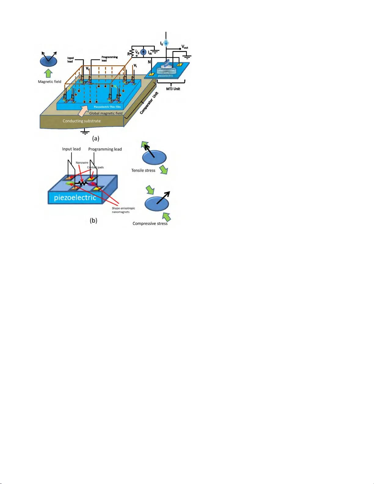
Applied Physics Letters(2015) Energy-efficient hyb rid spintronic-straintronic reconfigurable bit compa rato r Ay an K . Bisw as, 1 Jay asimha A tula simha, 2 and Supr iyo Bandy opa dhy ay 1 1) Dep artment of Ele ctric al and Computer Engine ering, Vir ginia Commonwe alth Uni versity, Richmond, Vir ginia 23284, USA 2) Dep artment of Me chanic al and Nucle ar Engine ering, Vir ginia Comm onwe alth University, Richmond, Vir ginia 23284, USA (Dated: 2 July 2021) W e prop ose a reconfigurable bit comparato r implemen ted with a nanowire spin v alve whose contacts a re magnetostrictive and po ssess bistable magnetization. Reference and input bits ar e “ written” into the magne - tization states o f the tw o co nt a c ts with electrically gener ated strain and the spin-v alve’s r esistance is low ere d if the bits match. Multiple compara tors can b e interfaced in parallel with a magneto-tunneling junction to determine if an N-bit input stream matc hes an N-bit reference stream bit by bit. The sy stem is robust against thermal noise a t ro o m temper a ture and a 16-bit comparator can op era te at ∼ 294 MHz while dissipating at most ∼ 19 fJ per cycle. Keywords: Co mparator , ener gy-efficient dig ital signal pro cessing, straintronics, nano ma gnets Digital sig nal pro cessing employing electron spins to store and pro cess bit infor mation offers certain adv an- tages over tr aditional charge-ba sed paradigms 1,2 . Here, we prop ose a hybrid spintronic-straintronic digita l r e- configurable N-bit co mparator that can op erate a t ro o m temper ature with reasonable speed while diss ipating v er y little energy . It is also “non-volatile”, meaning that the input bits, referenc e bits and the r esult of the bit stream compariso n (i.e. whether the input and reference bit streams ma tc h or not) can b e stor e d p ermanently in the magnetization states of magnets. Figure 1 (a ) shows the schematic o f an N-bit co mpara- tor fabr icated on a conducting n + -Si s ubstrate and a piezo electric lay er. A single bit compara tor blo ck is shown in the left panel o f Fig. 1(b) and cons ists of a nanowire “spin v alve” whose tw o fer romagnetic contacts are essentially tw o -phase multif er roics made of a magne- tostrictive material elas tica lly coupled to an under lying piezo electric film. The spacer layer of the spin v alve is a semiconductor nanowire in which electron transp or t is single-channeled and hence immune to D’yakono v-Perel’ spin relaxa tion 3 . Strong suppressio n of spin relaxation due to s ing le-channeled transp or t ha s b een obser ved in 50-nm diameter electro chemically self assembled InSb nanowires at ro om temperatur e 4 and pro g ressive sup- pression with decreasing width of a nanowire has be e n rep orted in InGa As nanowires 5 . T o fabricate the spin v alv e s tr ucture, a single ∼ 5 0 nm diameter InSb nanowire can b e ca ptur ed b etw een tw o lithog raphically delineated magnetostrictive contacts (depo sited on a piezo ele ctric film) using dielectropho resis 6 . The co n tacts are sha ped like elliptical disks and a global static magnetic field is directed along their mi- nor a xes. This makes the magnetiza tio n o r ientation of either co n tac t bistable . The tw o sta ble orientations lie in tw o a djacent quadra n ts in the ellipse’s plane b etw een the ma jor a nd minor a xes and subtend a n angle o f ∼ 90 ◦ with each o ther 7,8 as shown in the to p left co rner o f Fig. 1(a). Uniaxial tensile stres s of sufficient stre n gt h applied along one of these stable orientations will drive the mag- netization of a contact to that stable o rientation while compressive stress of sufficient strength will drive it to the other stable o rientation if the mag netostriction co ef- ficient of the co nt a c t mater ial is p ositive (the reverse will happ en if it is negative) 7,8 . This is shown in the right panel of Fig. 1(b). Two pairs of electrically shorted (non-magnetic) elec- tro des ar e als o delineated o n the piezo electric film, with each pair flanking a magnetostr ic tiv e contact such that the line joining the centers o f the electro des in a pair is approximately collinear with one stable mag netiza tion orientation of that contact [see left panel of Fig . 1(b)]. Application of a voltage (of appropr iate sign and mag- nitude) b etw een a n electro de pair and the underlying grounded n + -Si substrate will pro duce a tensile stress along the line joining the elec tr o de centers and a co m- pressive stress in the in-pla ne direc tion p erp endicular to that line 9 . V oltag e of the opp osite p olar it y will inter- change the signs of the stress e s 9 . This str essing scheme requires certain g eometrical co nstraints t o b e imp osed o n electro de size a nd separa tion, which a re describ ed in ref. [9] a nd not discussed here. In the end, b y a pplying a po sitive v olta ge at the electro de pair , we can ma ke the magnetization of the interposed mag netostrictive con tact of the spin v alv e o rient alo ng o ne stable direction, while by applying a negative voltage, we ca n make it orient along the other stable directio n. The wa y a sing le bit comparator works is as follows: First, a reference bit is “wr itten” a nd stored in the c om- parator by activ ating the electro de pair surro unding one magnetostrictive c o nt a ct of the spin v alve. This will ori- ent that c o nt a ct’s magnetiza tion alo ng one o f its tw o sta- ble s tates. Let us assume tha t the state attained when the electro de voltage is p ositive enco de s bit ‘1’ a nd the other state (attained when the electro de voltage is neg- ative) enco des bit ‘0’. Thus, a p ositive electro de voltage will write and store the bit 1 while a neg ative voltage will wr ite a nd stor e the bit 0. This electro de pair will bec ome the “prog r amming lea d” since it pr ograms the stored (r eference) bit. Since the sto red bit can be a lways Applied Physics Letters(2 0 15) 2 FIG. 1. (a) A strain tronic-spintronic m u lti- b it co mparator in- tegrated with a magneto-tunneling junction whose resistance indicates whether the input and reference bit streams match bit by bit. The MTJ unit and th e comparator unit share the same (grounded) conducting substrate although that has not b een sho wn explicitly in the fi gure for the sake of clar- it y . (b ) [Left panel] A single bit comparator unit showing the nanow ire spin v alve with magnetostrictive contacts fabricated on a piezoelectric lay er. The programming and inpu t leads are show n . [Right panel] Uniaxial tensile stress applied along one stable orientation of the nanomagnet takes the magneti- zation to that orientation while compressi ve stress takes the magnetization to the other orien tation. “re-pro grammed” with the programming lead, the co m- parator is r e c onfigur able . Next, to car ry out the bit com- parison, the voltage enco ding the input bit (po sitive volt- age = 1; neg a tive voltage = 0) is applied to the electr o de pair surr o unding the other co nt a c t o f the spin v alve (this electro de pair is ther efore called the “input lead”). If the input a nd the stored (reference) bits are the same, then the po larities of the voltages applied at the input lead and pro g ramming lead will hav e b een the same, mak- ing the magnetizations o f the spin v alve’s tw o contacts mutual ly p ar al lel . This will reduce the spin-v alve’s elec- trical resistance. O n the other hand, if the input and reference bits ar e different, then the ma gnetizations of the tw o contacts will b e in the t wo different orientations, which ar e roughly p er pendicula r, and the spin v alve r e - sistance will b e higher. Thus, the spin v alve’s r esistanc e is the indicator of match/mismatc h b etw een the input and reference bits. The ratio o f the res istances indicat- ing mismatch and ma tc h is 1 + η 1 η 2 1 (assuming no spin relaxatio n in the spacer lay er ), wher e the η -s are the spin injection and detection efficiencies of the t wo c o nt a cts. A t ro o m temp era ture, s pin injection efficiencies of ∼ 70% hav e been demonstra ted 10 ; therefore, this ratio can be ∼ 1.5 . Note tha t it would have b een further low er e d if there was s ignificant spin relaxa tion in the s pacer, which is why it is imp ortant to suppress relax a tion by ensur ing single channeled transp ort in the spacer layer. The ma gneto-tunneling junction (MTJ) unit in Fig. 1(a) is fabricated on the s a me (gro unded) conducting substrate and the piezo electric film as the spin v alve com- parator s. Its role is to deter mine if an N-bit input stream and a pre-progr ammed N-bit refer ence stream stored in the comparato r s match exactly bit by bit and store the re- sult (“yes” or “no ”) in its bistable r esistance sta te. The soft la yer of the MTJ is an elliptical magnetos trictive nanomagnet in elas tic co nt a ct with the underlying piezo- electric la yer and it ha s t wo stable magnetization o rien- tations that are roughly p erp endicular to ea ch other and lie in the plane of the so ft layer in t wo adjacent quad- rants b etw een the ma jor and minor axes , just like the magnetostrictive c o nt a cts of the spin v alves. The har d lay er of the MTJ is elliptical with v ery high ecce n tricity and its tw o stable states ar e roughly along the ma jor axis of the ellipse because of the very high shap e anis otropy . The ha rd na nomagnet is placed such that its ma jor axis is collinea r with one of the sta ble magnetization o r ienta- tions o f the soft nano magnet (resulting in a “skew ed MTJ stack” wher e the ma jor a xes of the tw o nanomagnets a r e at an a ngle). The hard na nomagnet is then mag ne tized per manently in a direc tion that is anti-p ar al lel to the stable magnetization direction of the so ft magnet. Th us, when the soft nano magnet is in one stable state, the mag- netizations of the hard and soft lay ers are a n ti-pa rallel (high MTJ res istance), while when the soft na nomagnet is in the o ther stable s tate, the ma g netizations of the tw o lay ers ar e r oughly p erp endicular (lo w MTJ resista nc e ). There are tw o contact pads flanking the MTJ and the line joining their centers is aligne d alo ng the mag - netization of the hard lay er (which als o happ ens to b e collinear with o ne stable magnetizatio n or ie n tatio n of the soft lay er). At the b eginning of any compar ison cycle , the MTJ resis tance is “reset” ; the soft layer’s mag netiza- tion is oriented in the sta ble direction that is anti-parallel to that of the har d lay er ’s b y applying a voltage of the appropria te p o larity b etw een the con tact pads and sub- strate [using co nnections not shown in Fig. 1(a) for the sake of clar it y] that generates tensile s tr ess in that direc- tion. The appr opriate p olarity dep ends on the direction of piezo electric po ling and the sign of the soft lay er ’s magnetostrictio n co efficient. O nce the reset o pe r ation is ov er, the MTJ is left in the hig h re sistance state. The wa y the MTJ unit works to determine match or mismatch b e t ween the input and refer ence bit str eams is Applied Physics Letters(2 0 15) 3 FIG. 2. Equiv alent circuit of th e N -bit comparator including the comparison and decision making units. as follows: O ne c ontact of each spin v alve is connected to a co mmon voltage source V I while the o ther contact is connected to one termina l of a passive resistor R whose remaining terminal is gr ounded as shown in Fig . 1(a). The corresp onding circuit is shown in Fig. 2. Using su- per p o sition, the v oltag e V 0 app earing acro ss the resistor R (and he nc e across the piezo electr ic layer underne a th the MTJ – see Fig. 1(a)) is found to b e V 0 = V I N X n =1 R n R n + r n , (1) where R n = R k r 1 k r 2 k · · · k r n − 1 k r n +1 k · · · k r N and r n is the resis tance of the n -th spin v alve. The ab ov e equation reduces to V 0 ≈ V I N X n =1 R r n = V I RG k if R n ≪ r n , (2) where G k is the s um of the spin v alve conductances ( G k = P N n =1 1 r n ). The strong inequalit y in the last equa tion is realistic since single nanowires tend to have very hig h resistances. It is easy to see now that when the input and reference bit streams match exactly bit by bit, the output voltage V 0 is maximum b ecause G k is maximum. W e ca ll this v alue of V 0 “ V match ”. When one o r more bits do no t match, V 0 < V match . Note tha t the voltage V 0 is applied at the MTJ elec- tro des. There is a threshold p ositive voltage V th which, when applied a t these electro des, will gener ate enough compressive stres s in the s oft lay er of the MTJ to ro- tate its magnetizatio n from the initia l (“res e t”) orienta- tion to the o ther stable o rientation that is roughly p er- pendicula r to the ma gnetization of the har d lay er. A t this thre shold voltage, the str ain energ y ov er comes the energy barrier betw een the tw o stable orientations to make the switching o ccur. This will abruptly take the MTJ from the initial (po st-reset) high-resistance state to the low-resistance state and reduce the res istance b y a factor of 1 / (1 − η 1 η 2 ). The MTJ is biase d by a co n- stant current source I 0 which generates a n output voltage V out = I 0 R M T J , where R M T J is the MTJ resistance. If V 0 ≥ V th , then V out is low (b ecause R M T J is low); other- wise, V out is hig h. W e will now set V match = V th . This will ensure that V out will be low if and only if the bit strea m and the reference str e am match exactly bit by bit. Otherwise, V out will be high. Thu s , b y monito ring V out , we ca n determine if the bit streams match ex a ctly . A compara tor of this type ha s been pr op osed earlie r by Datta et al. 11 where the magnets are switched with spin torque and no spin v alves a re used. There are t w o wa ys to ensure that the equality V match = V th holds. W e can design the soft lay er o f the MTJ (shap e, ma terial a nd dimensions) a s well a s the global mag netic field to make V th satisfy this equality , but it is c halleng ing to co nt r ol V th . An easier w ay is to fine tune V 0 with a v aria ble current source I dc as shown in Fig. 1(a). This will add an extra term I dc R to V 0 and change the r equired eq uality to V match + I dc R = V th . W e now do not ha ve to precisely craft V th . Instead, we will tune I dc to enforce the ab ove equality . All of the ab ove discussio n app ear s relev ant only to 0 K temp era ture when there is no thermal no ise to smear the sha rp V th . A t ro om temper ature, there will b e a broadening o f the threshold to V th ± ∆ V / 2. Therefore , to make the scheme work at ro om temper ature, we hav e to ensure that if even one bit do es not match , the re s ulting V 0 app earing acros s the resis tor R is consider ably less than V th − ∆ V / 2. This can be ensured by choo sing V I , R , I dc and the spin v alve resis ta nces in the low- and high- resistance states judiciously . First, we need to determine the smearing of V th by simulating the MTJ switc hing dyna mics at ro o m tem- per ature. W e assume that the soft lay er of the MTJ is made of T erfenol-D and shaped like a n elliptical disk o f ma jor axis 1 00 nm, minor axis 42 nm and thickness 16.5 nm. These dimensions ensure that the s oft nano ma gnet has a sing le domain 12 and the energy barr ie r b e t ween its t wo stable magnetiza tion sta tes is ∼ 7 3 kT at ro om tem- per ature if the glo bal magnetic field is 0 .14 T esla 13 . The stress g enerated in the soft nanomag net by a given volt- age applied at the MTJ ’s electro de pair is estima ted from ref. [9] assuming that the piez o electric layer is a 10 0- nm thick lea d- zirconate-titana te (PZT) film. W e simu- late the magneto dynamics of the soft nanoma gnet under stress in the presence of ther mal noise in the manner o f refs. [14] and [15], i.e. by simu la ting switching tra jecto- ries a ccording to the sto chastic Landau- Lifshitz-Gilber t (LLG) equation 19 . When the soft layer switches from one stable ma g netization sta te to the other, the MTJ re- sistance changes by a fa ctor of 1 / (1 − η 1 η 2 ) ≈ 2 if we Applied Physics Letters(2 0 15) 4 FIG. 3. Switching characteristic of the MTJ switc h R ( V ) ver- sus V in the presence of thermal n oise at ro om temp erature. This plot is generated by simulating 10 5 switc hing tra jecto- ries in th e manner of refs. [14] an d [15] to find the thermal spread in the switching th reshold. assume η 1 = η 2 = 0 . 7 10 . Higher resistance r atios exceed- ing 6:1 ha ve b een de mo nstrated at r o om temper a ture 18 , but we will b e conser v ativ e a nd a s sume the ratio to b e 2:1. Fig. 3 shows the resistance R ( V ) /R low versus V where R ( V ) is the MTJ re sistance when a voltage V is applied at the electro de pair a nd R low is the low re- sistance o f the MTJ . T o generate this s catter plot, 1 0 5 switching tr a jectories were simulated at ro o m temp er- ature. Clearly , r o om-temp erature fluctuations broaden the switching threshold by ∼ 2 2 mV (i.e. ∆ V = 22 mV), and switching can o ccur anywhere b etw een 75.6 and 97.6 mV applied at the MTJ’s electro de pair. W e will now hav e to ensure that when all bits in the in- put a nd refer ence streams match, V 0 = V I RG max k + I dc R ≥ 97.6 mV, a nd when there is just one mismatch, V 0 = V I RG 1 − mismatch k + I dc R ≤ 75.6 mV. W e ensure this by choosing V I = 10 V, I dc = 1.51 µ A, R = 1.525 MΩ, low r esistance of the spin v alve 100 MΩ and high res is- tance 15 0 MΩ. These choices r esult in V I RG max k + I dc R = 110.19 mV and V I RG 1 − mismatch k + I dc R = 69 .67 mV. Thu s , even at ro om temp erature, we can detect a sing le bit mismatch b etw een the tw o streams with a probabil- it y exceeding 99.999 9% (since 10 5 switching tra jectorie s were simulated). The sto chastic LLG equation also a llows us to deter- mine the switching time and the energ y dissipa ted dur ing switching of a n y mag ne to strictive na nomagnet (whether it is the MTJ’s soft lay er during decision making, or the spin v alv e’s contacts during writing o f r eference and in- put bits) in the pr esence of ro om-temp eratur e ther ma l noise 14–17 . Fig . 4 shows the ro o m-temper ature mag - netization dynamics , i.e. the ma g netization orientation (represented b y the angle θ tha t the magnetiza tio n vector subtends with a na nomagnet’s ma jor axis) as a function of time a fter a voltage V = V 0 = 110 mV is applied to a pair o f ele c tr o des to g enerate s tress in a magnetostrictive nanomagnet and initiate switchin g . The voltage is a p- plied abruptly at time t = 0 and withdrawn abruptly at time t = 1.2 ns . The stress duration of 1 .2 ns ensures that all 10 5 tra jectorie s simulated switch successfully (switch- ing error pro babilit y < 10 − 5 ). F or each tra jectory , the magnetization vector starts out fro m ar ound the s table state at θ = 45 ◦ and switches to a state that is aro und the stable state at θ = 13 5 ◦ . Beca us e of ther ma l no ise, there is so me fluctuation of the initial state a round θ = 45 ◦ and the final state around θ = 13 5 ◦ . The temp or al charac- teristics for arbitrar ily pick ed 1000 switching tra jecto ries are plotted in Fig . 4. The max imum time it ta kes for any tra jector y to switch is 1.15 ns. FIG. 4. Switching dyn amics of a nanomagnet in the p resence of room-temp erature thermal noise. A v oltage is applied to the electro des abrup tly at time t = 0 and withdrawn abruptly at time t = 1.2 ns. The initial orien tation of the magnetiza tion is near one stable state at θ = 45 ◦ and the fi nal orientation is around the other stable state at θ = 135 ◦ . There is some fluc- tuation around these states o wing to th ermal noise. All 10 5 tra jectories simulated switch within 1.15 ns. The plot shows arbitrarily pic ked 1000 tra jectories. Here, thermal fluctua- tions are not considered after switching. The energ y dissipated dur ing switching ha s tw o co n- tributions – internal dissipatio n due to Gilb er t damping in the nanomag ne t and (1 / 2 ) C V 2 dissipation as so ciated with charging a nd discharging the ele ctro de capacitances non-adiabatica lly . The former contribution is found to be 1.45 a J (after av er aging ov er 10 5 switching tra jectorie s ) 17 and the latter is 10 .64 aJ sinc e V = V 0 = 11 0 mV and C for e a ch of the tw o electro des is 0 .88 fF based on elec- tro de area of 100 nm × 10 0 nm a nd P ZT layer thick- ness of 10 0 nm (the rela tive dielectric constant of P Z T is roughly 1,0 00). There fore, the to ta l energy diss ipated to progra m a r eference bit, o r write an input bit, is ∼ 12.1 Applied Physics Letters(2 0 15) 5 aJ. In a 16 -bit co mparator , the energy dissipa ted to pro- gram 16 r eference bits (o r write 16 input bits) will b e 16 × 12 .1 aJ = 19 3.6 aJ. Even if a refere nce bit (or input bit) do es not change from the previo us cycle, we will not know that a pr iori since we do not read the s tored bit. Therefore, we will hav e to rewrite every bit and th us all 16 reference bits will hav e to b e r eprogr ammed and all 16 input bits will hav e to b e rewritten. The ene r gy dissipated to switch the soft layer of the MTJ (and hence make its resista nc e s w itch) is obviously also ∼ 12.1 aJ. The time to charge the capacitance in the MTJ unit is τ = R eq C, where R eq = R k r 1 k r 2 k · · · k r 16 = 1.2 2 MΩ. Hence, the RC time constant asso ciated with charging turns out to b e 1 ns. In addition to the ener gy dissipated during switc hing, there is dissipation caused by the cur rent a nd voltage sources in the spin v alv e r esistances r n , the bia s res is- tance R , and the MTJ resistance R M T J . W e can tur n on the current and voltage sources only when a n in- put bit strea m arrives in or der to avoid standby energy dissipation. W e will keep V I and I dc on for the dura- tion t ON = 1.2 ns and I 0 on for the switc hing dura - tion t s to ensure b oth corr ect decision making and cor- rect reading of the decis ion with > 99 .9999% proba bility . The energ y dissipated in the n -th spin v alve is a t mo s t (( V I − V 0 ) 2 /r low n ) t ON = (9.89 V) 2 × 1.2 ns /100 MΩ = 1.17 fJ during the compar ison op eration and so in a 16 bit comparato r, this dis s ipation is 18.7 fJ. The energ y dis- sipated in the resistor R is ( V 2 0 /R ) t ON = (110 mV) 2 × 1.2 ns /1 .525 MΩ = 9 .5 aJ. The ener gy dissipated in the MTJ is I 2 0 R M T J t s which can b e ma de arbitra rily small by ma k ing I 0 arbitrar ily small. Ther efore in a complete cycle consis ting o f pr ogra mming all 16 bits, r eceiving 16 inputs a nd then compar ing the pro g rammed bits with the input bits, the total energy dis sipation is 193 .6 aJ + 193.6 aJ + 12 .1 a J + 18.7 fJ + 9.5 aJ = 1 9 .1 fJ. The total time r equired to progr a m 16 bits while rece iving 16 input bits at the same time (and als o “resetting” the MTJ at the sa me time) is 1.2 ns, the time required to pro duce the decision (match or no match) by switching the MTJ resistance after the compa rison is over is another 1.2 ns (to ensure that the err or probability is less than 10 − 5 ), and the additional capa citor charging time is 1 ns, r esult- ing in a total delay of 3.4 ns. Therefor e, the maximum op erating sp eed is 1/3 .4 ns = 294 MHz. In conclusion, we hav e pro p os ed and analyze d a spintronic-straintronic re c onfigurable N-bit comparato r (whic h uses s pin prop erties for device functiona lit y and strain to switch the device) and shown that it is remark - ably e ne r gy-efficient, r e la tively error-re silient and reaso n- ably fast a t ro om temp eratur e. Such compara tors ha ve the additional adv antage that the re s ult of the compar- ison can b e sto r ed indefinitely in the resistance state of the MTJ, resulting in non-volatility . This work was supp orted by the US Nationa l Sci- ence F oundation under grants ECCS-1 1247 1 4 and CCF- 12166 14. J. A. would also like to a c knowledge the NSF CAREER grant CCF-1253 370. 1 S. Bandyop adhy ay and M. Cahay , Intr o duction to Spintr onics (CR C Press, Boca Raton, 2008). 2 S. A. W olf, D. D. Awschalom, R. A. Buhrman, J. M . Daughton , S. von Molnar, M. L. Roukes, A. Y. Chtc helk ano v a and D. M. T reger, Science 294 , 1488 (2001). 3 See, for example, S. Pr amanik, S. Bandy opadh ya y and M. Caha y , IEEE T r ans. Nanotec hnol. 4 , 2 (2005). 4 S. Bandy opadh ya y , Md. I Hossain, H. Ahmad, J. Atulasimha and S. Bandy opadhy a y , Small 10 , 4379 (2014). 5 A. W. Holl eitner, V . Sih, R. C. Myers, A. C. Gossard and D. D. Awsch alom, Ph ys. Rev. Lett. 9 7 , 036805 (2006). 6 D. Xu, A. Subramanian, L. X. Dong and B. J. Nelson, IEEE T rans. Nanotechn ol. 8 , 449 (2009). 7 N. Tier celi n, Y. D usch, V. Pr eobrazhensky and P . Pernod, J. Appl. Phys. 109 , 07D726 (2011). 8 S. Giordano, Y. Dusch, N. Ti ercelin, P . Pernod and V . Preo- brazhensky , Phy s. Rev. B 85 , 155321 (2012) 9 J. Cui, J. L. Ho ck el, P . K. Nor deen, D . M. Pis ani, C. Y. Liang, G. P . Carman and C. S. Lync h, Appl. Phys. Lett. 103 , 232905 (2013). 10 G. Salis, R. W ang, X. Jiang, R. M . Shelb y , S. S. P . Parkin, S. R. Bank and J. S. Har is, A ppl . Phy s. Lett. 87 , 262503 (2005). 11 S. Datta , S. Salahuddin and B. Behin-Aein, Appl. Ph ys. Lett. 101 , 252411 (2012). 12 R. P . Cowburn, D. K. Koltso v, A. O. Adeyey e, M. E. W elland and D. M. T rick er, Phy s. Rev. Lett. 83 , 1042 (1999). 13 M. Beleggia, M. De Graef, Y. T. Millev, D. A. Goode and G. Ro wl ands, J. Phys. D: Appl. Phys. 38 , 3333 (2005). 14 K. Ro y , S. Bandy opadhy a y and J. Atulasimha, J. Appl. Ph ys. 112 , 023914 (2012). 15 A. K. Biswas, S. Bandy opadhy a y and J. Atulasimha, Appl. Phys. Lett. 104 , 232403 (2014). 16 W. Scholz, T. Sch r efl and J. Fidler, J. Mag. Mag. Mat. 233 , 296, (2001) 17 T. V. Lyutyy , S. I. Denisov, A. Y . Pelet skyi, and C. Binns, arXiv:1502.04222v1[cond-mat.mes-hall] (2015). 18 S. Ikeda, J. H a yak a wa, Y. Ashizaw a, Y. M. Lee , K. Miura, H. Hasega wa, M. Tsuno da, F. M atsukura and H. Ohno, Appl. Phys. Lett. 93 , 082508 (2008). 19 F. M. Sp edalieri, A. P . Jacob, D. E. Nikono v and V. P . Roy - c howdh ury , IEEE T r ans. Nanotec hnol. 10 , 537 (2011).
Original Paper
Loading high-quality paper...
Comments & Academic Discussion
Loading comments...
Leave a Comment