Erase-hidden and Drivability-improved Magnetic Non-Volatile Flip-Flops with NAND-SPIN Devices
Non-volatile flip-flops (NVFFs) using power gating techniques promise to overcome the soaring leakage power consumption issue with the scaling of CMOS technology. Magnetic tunnel junction (MTJ) is a good candidate for constructing the NVFF thanks to …
Authors: Ziyi Wang, Zhaohao Wang, Yansong Xu
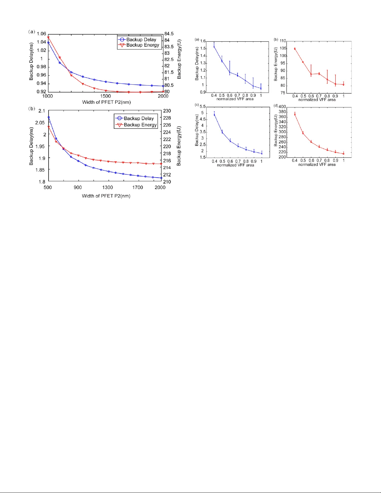
> REPLACE THIS LINE WI TH YOUR PAPER IDENT IFICATION NUM BER (DOUBLE - CLICK HERE TO EDIT) < 1 Abstract — Non-volatile flip-flops (NVFFs) using power gating techniques promise to overcome the soaring leakage power consumption issue with the scaling of CMOS tec hno logy. Ma gnetic tunnel junction (MTJ) is a good candida te for constructing the NVFF thanks to its low powe r, high speed, good CMOS compatibility, etc. In th is paper, we propose a novel magnetic NVFF based on an emerging memory device called NAND-SPIN. The data writing of NAND-SPIN is a chieved by successively applying two unidirectional currents, which respectively generate the spin orb it torque (SOT) and spin transfer torque (STT) fo r erase and pro gramming o perations. This characteristic allo ws us to design an erase-h idden and drivability -improved magnetic NVFF. Furthermore, more design flexibility could be obtained since the backup operation of the proposed NVFF is not l imited by the inherent slave latch. Simulation results show that our p roposed NVFF achieves performance improvement in term s of power , delay a nd area, compared with conventional sl ave-latch-driven SOT-NVFF designs. Index Ter ms — Non-volatile flip-flo p, NAND-SPIN, spin orbit torque, spin transfer torque, magnetic tunnel junction I. I NTRODUCTION S key units in digital system s, flip-flops (FFs) store computing data for the central processing unit (CPU), micro controller unit (MCU), and so on. However, with CMOS technology scalin g down, leakage po wer of the conventional flip-flops is b ecoming more and mo re sign ificant [1][2]. In a microprocessor, the leakage power may exceed 40% of the total system po wer b elow 65 nm technology nod e [3 ]. Power gating (PG) technology, which makes the inactive circuits disconn ected from the p ower supply in the standby mode, is a popular solution to eliminate the leakage po wer [4][5] . Nevertheless, the conven tional CMOS FFs cannot r etain the data d uring the power off , thus the data have to be backup into the main memory or disk drivers before triggering the PG , which result s in additional speed and energy ov erhead. These bottlenecks can b e overcome by designing a non -volatile flip- flop (NVFF) [6]-[11], which is a hybrid a rchitectu re comb ining the conventional CMOS FF with th e emer ging non -volatile Ziyi Wang, Yansong Xu and Bi Wu are with the School of Electronics and Information E ngineering, Beihang Un iversity, Beijing 100191, China. Zhaohao Wang and Weisheng Zhao are with School of Microelectronics , Beijing Advanced Innovation Center for Big Data and Brain Computing memories (NVMs). While the PG i s ac tivated in a NVFF, t he data can b e b ackup into the local NVMs rather than be moved to the other modules. Thus, add itional cost in the speed an d energy could be avoided. Amongst the NVFFs, magnetic NVFFs employing m agnetic tunnel jun ction (MTJ) have been paid m uch attention due to high speed , low p ower, unlimited endur ance and go od CMOS compatibility [11]-[26]. Spin transfer torque (STT) is most widely used for th e write operation of the MT J [27] -[30], an d hence for the backup operation of th e magnetic NVFF. However, the performance of the STT -NVFF s i s deteriorated by the asym metry o f backup operation between two write directions, which is attributed to the asymmetr ical STT switching efficiency . In ad dition, the backup operation requires a pair of opposite currents to w rite ‘0’ and ‘1’, respectively , thus the source degeneration effect d egrades the drivab ility of the related transistors, due to the different gate-sou rce biases while writing ‘0’ and ‘1’ [31] . As a result , the transistors ha ve to be large enough to tolerate the worst case of two switching even ts . However, it would induce overlarge current for the othe r case , which incurs larg er energy dissipation and threatens the reliability of the dev ices . Although spin orb it torque (SOT) have been recently exp lored as an alter native to the STT [32]- [34], the source degener ation effect remain s unresolv ed in the SOT-NVFF since the SOT switching cu rrent is still bi- directional. In the mo st of the area-efficient mag netic NVFFs, the MTJs are direc tly switched b y a pair of co upled CMOS inver ters in the slave latch du ring the backup op eration [21], [23] , [25], [30] . Large-size tran sistors are requ ired to ensur e the driv ability of the slave latch, which may degrade the p erformance of the CMOS part (i.e. volatile flip-flop structure) . Moreover, most of the SOT-NVFFs emplo y two complementary SOT-MTJs to store 1-bit non -volatile data. The current channels (i.e. the heavy metal b elow the MTJ) have to b e oppositely placed so that the MTJs are always written into the complementary states [11], [19], [23], [25], [ 26] . This type of layout will lead to difficulty in the practical fabrication pr ocess. To overcom e th e af orementioned drawbacks of both STT - NVFFs and SOT-NVFFs, in th is pap er we propose an erase- (BDBC), Fert Beijing Research Institute, Beihan g Univer ti sy, Beijing 100191, China (e-mail: zha ohao.wang@buaa.edu .cn; weisheng.zhao@buaa. edu.cn). Erase-hidden and Drivability-improved Magnetic Non-V olatile Flip Flops with NAND - SPIN Devices Ziyi Wang, Zhaoh ao Wang, Member, IEEE , Yansong X u, Bi Wu, and Weisheng Zhao, Fellow, IEEE A > REPLACE THIS LINE WI TH YOUR PAPER IDENT IFICATION NUM BER (DOUBLE - CLICK HERE TO EDIT) < 2 hidden and drivability- improved magnetic NVFF based on a high-p erformance magnetic memo ry structure ca lled NAND- SPIN [3 5]. Gen erally, the data is written into th e NAND -SPIN by applying two unidir ectional curr ents, which perform a SOT- induced erasing and a STT -driven programing, respectively. The erase o peration is hid den into the ac tive mode to redu ce the backup delay. Furthermore, the source degen eration effect is eliminated thanks to th e use of unid irectional switching currents. More impo rtantly, the proposed NVFF relaxes the requ irement on the drivability of the inherent slave latch , and therefore allows a more flexib le design . Two embodiments o f the proposed NVFF, wh ich uses p erpendicular - an d in-plane- anisotropy MTJs, ar e designed and simulated with an electrical model of the SOT- MTJ and CMOS 40 nm design k it . Comparison among various NVFFs is shown based on the simulation results. The r emainder of this pap er is o rganized as follows. Section II introduces the fundamentals of NAND-SPIN devices. In section III, we elaborate th e circuit structure and operation of the pro posed NVFF . The simulation resu lts are d iscussed and evaluated in sectio n IV . An exten sion work is described in section V. Finally , section VI conclu des this paper. II. F UNDAMENTAL OF NAND -SPIN D EVICE The NAND-SPIN device used in this work is composed of two MTJs and a heavy-metal strip, as shown in Fig . 1. An MTJ comprises of two ferr omagnetic lay ers, called free lay er (FL) and pinn ed layer (PL), separated by a tun neling o xide bar rier. The magn et ization of the PL is fixed whereas the FL magn et ization can be switched between par allel and antiparallel (P an d AP) to that of the PL, corresponding to low and high tunnel resistances, respectively . Two MTJs of the NAND-SPIN device are always switched to complem entary resistance states, which repr esents 1-bit non-v olatile data. Here the MTJs are switched by a SOT- induced erasing and a STT-driven programing. The detailed operation is descr ib ed as follows [35]. First, a current is ap plied to the heavy metal and induces the SOT, which switches both the MTJs to AP states. Thus, this step is called erase operation. Then the programming operation is perfor med. The SOT curren t is turned off, and another current flowing th rough o ne MTJ will switch it to P state by the STT. The other MTJ remains at AP state. As a result, two MTJs are switch ed to P an d AP states, respectively. Depending on the relativ e states between two MTJs, th e data ‘0’ or ‘1’ is stored . Compared with th e conventional STT - or SOT -MTJs, NAND -SPIN shows extraord inary properties in energy efficiency and area efficiency for t hr ee reasons. First, AP and P states are respectively written by the SOT and STT. Th erefore, the write currents are unidirectional, wh ich allows more compact circuit structure and avoids the source deg eneration of the tran sistors [3 1]. Second, the asymmetry of the STT is alleviated since the STT is only used for the easier AP- to - P switching. Third, NAND -SPIN device could be fabricate d as a whole by self-aligned process [36], which simplifies the procedure and improves the integratio n density. An electrical m odel of NAND-SPIN is developed for the simulation an d evaluation in this paper . The resistance of the MTJ is modeled by Brinkman model, bias- dependent tunneling magnetoresistance effect, Slonczewski mod el, etc. More details could be found in [ 37]. The m agnetization switching is described by a Landau-Lifsh itz-Gilbert (LLG) equation , which considers bo th the STT and SOT, as where and are the un it vectors along the magn etization orientation of the FL an d PL, respectively. is th e polarization direction of the SOT-ind uced spin accumulation . and are the STT and SHE write cur rent densities, respectively. is the effective magnetic field. is the gyromagnetic ratio, is the vacu um permeability , with the reduced Planck constant, the TABLE I S IMULATION P ARAMETE RS Parameters iMTJ device [ 19 ][21][ 23 ][ 38 ] pMTJ device [19][35] [ 38 ][ 39] Free layer volume Dimensions of W strip ( ) Damping consta nt ( ) Resistance-area product ( ) Saturation magnetization ( ) Spin Hall angle ( ) 0.3 0.3 Tu nneling spin polarization ( ) 0.62 0.62 TMR ratio 120% 120% Heavy metal resistivity ( ) Thermal stabilit y barrier ( ) Asymmetrical STT efficie ncy ( ) 1.3 1.3 Bias magnetic fie ld ( ) - -0.005/ Fig. 1 S chemati c structure and operation currents of a p -NANS-SPIN device. > REPLACE THIS LINE WI TH YOUR PAPER IDENT IFICATION NUM BER (DOUBLE - CLICK HERE TO EDIT) < 3 elementary charge, and the thickness of the FL. Othe r parameters ar e exhibited in Table I . The asymmetr y of the STT is reflected by , as where is a factor [38]. The larger induces more asymmetrical STT efficiency between two switching directio ns. will eliminate the asymmetry of the STT. III. P ROPOSED NVFF D ESIGN WITH NAN D-SPIN This section presents the schematic and operation of the proposed NAND-SPIN b ased NVFF using both perpendicu lar- and in-plane-anisotropy MTJs (named as p- NAND -SPIN and i- NAND -SPIN). NVFF s tar geting PG arch itectures cou ld work in four modes: active, bac kup, standb y, and restore mo des. In the active mode, the NVFF operates as a normal volatile flip - flop (VFF) . Before triggering the PG, the volatile d ata need to be written into the non- volatile NAND-SPIN in the backup mode. Then th e power supply co uld be t urned off in the standby mode to avoid th e leak age power. Once the power supply is restarted, the non -volatile data inside the NAND -SPIN n eed to be written back to the volatile flip-flop in the restore mode. As mentioned in Section II, the data is written into the NAND - SPIN through an erase operation an d a program ming operation. It is wo rth notin g that the polarity of the written d ata is determined by the program ming operation rather than the erase operation. Th erefore, we intentionally hide the er ase o peration inside the active m ode so that on ly programming operation occurs in the backup mod e. With this erase-hid den design , th e backup laten cy is redu ced, mea nwhile th e size of driving transistors could be tuned more flexibly. A. Circuit Operation The schematic of the p -NAND-SPIN NVFF is illu strated in Fig. 2 (a), including a CMOS -based VFF part (outside the dashed region) and a NAND-SPIN based non -volatile part (inside the dashed region). A slave latch is comb ined with o ne NAND -SPIN and six additional transistors (P1-2 and N1-4) for data retention during the standby mode. This non-volatile slave latch is connected with a clocked CMOS master latch to form the NVFF. The i- NAND -SPIN NVFF is not shown here for the simplicity, because it can be designed with th e same stru cture as Fig. 2(a) except for the anisotropy direction of th e MTJ. (a) (b) (c) (d) (e) Fig. 2(a)The schematic of t he prop osed p-NAN D-SPIN NVFF. (b) Erase operation of the p-NAND-SPIN NVFF. Here the orange-colored components are activated, i.e. the erase operation is hidden in the active mode. (c) Restore operation of the p -NAND- SPIN NVFF. (d) Backup ‘1’ operation of the p-NAND- SPIN NVFF. (e) Backup ‘0’ operation of the p -NAND-S PIN NVFF. > REPLACE THIS LINE WI TH YOUR PAPER IDENT IFICATION NUM BER (DOUBLE - CLICK HERE TO EDIT) < 4 During the active mode, as shown in Fig. 2(b), EQ = ‘1’ , Ctrl = ‘0’ and REN = ‘0’ , thus P1 , N1 and N3- 4 are deactivated. As a result, the NVFF acts as a C MOS-b ased VFF wh ich is iso lated from the NAND -SPIN. Once th e NVFF just en ters the active mode, transistor s P2 and N2 is turn ed on for a short time to initializ e the NAND- SPIN to state ‘11’, which means that two MTJs are initialized to AP state s (i.e. the erase operation mentioned above) . This erase operation of the NAND-SPIN does not interfere with the normal operation of CMOS-b ased VFF due to the disconnected structure . As a result, the erase operation is h idden inside the active mode withou t additional latency. Before the system en ters the standb y mode th rough the PG technology, the run time data in the NVFF need to be backup into the NAND -SPIN. To perform a bac kup, the CTRL sign al and the PSL signal are asserted high, th e CLK signal holds low fo r storing data i n to the slave latch. As mentioned above, both MTJ1 and MTJ2 have been erased to AP states during the active mod e. T hus, one of two MTJs nee ds to be switched to P state for comp leting the backup. Assum e QT = ‘1’ and QC = ‘0’ , as shown in Fig. 2(d), transistors P2 and P6 work together as the current source, wh ile transistor N5 acts as th e curren t sin k. Two cu rrents (I w1 and Iw2) driven by P2 and P6 are applied to the NAND-SPIN. As a result, MTJ2 is switched to P state through the STT, meanwhile MTJ1 rem ains at AP state. Similarly, if QT = ‘ 0’ and QC = ‘1’ (see Fig . 2 (e)), MTJ1 and MTJ2 are respectiv ely set to P and AP states. In summary, d epending on the level o f QT/QC, t he two MTJs of the NAND -SPIN are pro grammed to complemen tary states ‘P/AP’ or ‘AP/P’ during the backup mode. It is impor tant to mentio n that the STT is only responsible for AP- to -P switching, which requires smaller current and shorter latency compared to P - to -AP switching . The restore operation is illustrated in Fig. 2(c). Once the power supply is restarted, EQ is kept at low level so that transistor P1 sho rts QT and QC, and thu s the power supply charge QT and QC to . Me anwhile the sign al REN is pulled down and transistor N1 is open . Thus, QT and QC start discharging to form two read currents (Ir1 and Ir2) passing through MTJ1 and MTJ2, respectively. At this time th e signal EQ is pulled up again to isolate QT from QC. As MTJ1 and MTJ2 h ave been written into comp lementary states durin g the backup mode, the discharg ing in the low MTJ resistance branch is faster than that in the other b ranch. As a result, the node on the low MTJ r esistance branch dr ops to ground and the o ther node is pulled u p to VDD . In this way, the complementary states in th e NAND - SPIN are restore d to the slave latch of VFF. B. Advan tages of the Proposed NVFF Generally, m ost of the SOT-NVFF arch itectures rely on the inherent slav e latch to achieve the bac kup operation . However, these ar chitectures ex hibit p oor p erformance in backup delay and energy consumption. Below we will demonstrate how our proposed NVFF im proves the speed an d energy efficiency. For the existing SOT-NVFFs, the polarity of the written data is depen dent on the direc tion of the applied current. Therefore, bi -directional current need to be g enerated by the dr iving circuits. A common solution is to construct an independent write dr iver with additional four transistors [19 ], [20] , but it leads to large area overhead. To achieve an ar ea-efficient design , this bi- directional cu rrent is mo stly provid ed by an inherent slave latch (e. g. transistors P5-6 an d N5-6 in Fig. 2). To ensure sufficient write current, the transistors of the s lave latch have to be larg e, which may deg rade the performance of CMOS-based VFF par t, such as large ar ea ov erhead an d stron g parasitic effects. In contrast, our proposed NVFF employs unidirectional current to ac hiev e the backup oper ation. Thus, the write current could be directly provided by the power sup ply rath er th an the slave latch. Only two access transistors (P2 and N2 in Fig. 2 ) are add ed for the efficient contr olling. Furthermore, transistor P2 shows the largest drivability since it is directly connected to the power supply t o ma ximize its source -gate bias (i.e. t he source degeneration effect is eliminated) . The same ben efit is obtained by transistor N2 during the er ase operatio n, as the unidirection al current is direc tly injected to g round. Thanks to this novel design, the current for the backup operation could be TABLE II C OMPARISON AMONG THE VARIOUS NVFF S . Parameter p- y type i- y type [23] [25] p- x type i- x type Delay (ns) Backup 1.04 1.87 4.95 4.32 0.99 1 .8 68 Restore 0.66 0.66 0 .6 6 0 .6 6 0 .6 6 0 .6 6 Energy (fJ) Backup 84.3 216.5 281.7 239.5 84.1 216.4 Erase 8 4. 1 1 19.9 - - 196.0 229.2 Restore 56.0 54 .0 67.6 53.0 58.4 64.4 The trans istor sizes of PFET and NFET in VFF part of all N VFFs above are set to 400/40 and 29 0/40, respectively. I n the p ropose d NVFF s (p -y type, i- y type, i-x type), the driving transistor P2 is set to 1000/40 ; in the p ro posed p -x type NVFF, the driving transistor P2 is set t o 2000/40 to ensure a successful erase. The definitions of x- type and y-type will b e described in Section V. Fig. 3 Timing diagra m of the proposed p -NAND-S PIN NVFF. The MT J1 and MTJ2 signals are normalized z-compone nt magnetization of the free layer. Othe rs are voltage sign als. > REPLACE THIS LINE WI TH YOUR PAPER IDENT IFICATION NUM BER (DOUBLE - CLICK HERE TO EDIT) < 5 tuned by adjusting transistors P2 and N2, not limited by the size of the slave latch . In addition, som e SOT -NVFFs emp loy a p air o f oppo sitely- placed SOT-MT Js to store complementary states [1 1], [19], [23], [ 25], [ 26] . However, it causes the d ifficulty of manufacture since two SOT-MTJs have to be etched in the opposite po sition. In our proposed NAND -SPIN based N VFF, two MTJs share the sam e heavy metal strip which could be easily fabricated by self-aligned etch ing process [36] . IV. R ESULTS AND D ISCUSSION In this sectio n the pr oposed NVFFs are simulated wi th a CMOS 40 nm desig n kit and a SOT- MTJ model mentioned in section II. The comparison of perform ance among vario us NVFFs is shown based on the simulation results. The optimization strategy of the p roposed NVFF is discussed by investigating th e roles of key parameters. A. Evaluatio n of Different SOT ba sed NVFF Architectures Fig. 3 shows the transient simu lation results of the pr oposed p- NAND -SPIN NVFF. The sig nal wav eforms r eproduce the behavior s of th e four operation modes described in section III - A. The timing diag ram of i - NAND -SPIN NVF F can b e obtained in a similar way, thus it would not be presented here for the simplicity . Two NVFFs presented in [23] and [25] are cho se as th e baseline fo r co mparison, because they showed more excellent performance than the existing other pro posals. For a fair comparison , the same model and parameters are u sed among the various NVFFs. The detailed co mparison results ar e listed in Table II. The proposed i- NAND -SPIN NVFF design offer s 10 % lower backup energy with nearly 43 % red uction o f the backup delay compared to [2 5]. This improvement is mainly attributed to two reasons: first, in the i- NAND -SPIN NVFF the magnitude of the write curren t is not limited by the slave latch. In stead larger write current could be driven by the transistor P2. Second, only AP - to - P STT switching is performed in the backup mode, which costs smaller energy and shorter delay than the P- to -A P case due to the asymm etrical STT eff iciency . For instance , P- to -AP STT switching d elay of the proposed p- NAND -SPIN NVFF is as larg e as ~5.7 ns under the above parameter settings. Thus, in our proposed NAND -SPIN NVF F the AP state is written by the SOT -induced erase operatio n rather than the S TT for avoiding the excessive co st in the speed and energy. I n addition, the proposed i- NAND -SPIN offers 23% lower energy and 2.6 × fa ster backup speed co mpared with [23], using the same operatio n mechanism. As fo r the pro posed p -NAND-SPIN NV FF, 65 % lowe r backup energy and 4.2 × faster backup speed can be achieved compared with [25] . The improvemen t is more significant than the case of i- NAND -SPIN NVFF, which is attrib uted to the fact that the perpendicular- anisotropy optimizes the STT efficiency. It should be p ointed ou t that concealment of erase operation also lar gely r educes delay and energy during the per iod of backup . All the NVFFs mentio ned above perform a r estore operation in the same way , thus few er differen ces can be seen from the comparison shown in Table II. B. Drivability an alysis on the Prop osed NVFF As mentioned ab ove, the currents fo r the backup o peration mainly arise from the driving transistor P2 rather than the inherent slave latch. Ther efore, more design flexibility cou ld be Fig. 4 Backup p erf ormance as a f unction of P2 t ransistor size with PFET/NF ET of VFF set to 400/290. (a) p - NAND -SPIN NVFF (y-type) (b) i - NAND -SPI N NVFF (y-type). Fig. 5 The change of backup performance with the scaling of VFF area, and VFF area is normalized to the standard area with PFET/NFET = 400/300. H ere the standard a rea is evaluated t o be 1.6 3.9 according to CMOS 40 nm design kit. (a)-(b) p- NAND -SPIN NVFF (y -type); (c)-(d) i- NAND -SPIN NVFF (y -type). The error bar indicates the range of backup performance while varying the P2 size. > REPLACE THIS LINE WI TH YOUR PAPER IDENT IFICATION NUM BER (DOUBLE - CLICK HERE TO EDIT) < 6 obtained. Here we study the backu p performan ce as a function of P2 trans istor size, as shown in Fig. 4 . Given a f ixed VFF area, we observe th e change of b ackup performance by sweeping the width of the drivin g transistor P2 in both p - and i- NAND -SPIN NVFFs. As shown in Fig. 4(b), when the wid th of P2 varies from 500nm to 2000 nm, the backup delay and energy of i- NAND -SPIN NVFF are reduced by 12.4% and 5%, respec tively. Similarly , as sho wn in Fig. 4(a), they decrease by 10.2% and 5% when the width of P2 changes from 1000nm to 2 000nm in th e p - NAND -SPIN NV FF. This tendency could be easily understood since P2 acts as a cur rent source offering the backup current. From th e results, a trade -off could be obtained b etween the backu p performance and P2 size: faster and more energy -efficient backup operation of NAND - SPIN NVFFs requir e a larger P2. C. Performan ce of the Propo sed NVFF with CMOS -based VFF Scaling In addition to the driving transistor P2 , the CMOS-based VFF part also h as a non-negligible influence the backup performance. Figures 5-6 shows the backup p erformance as a function of th e various VFF area. At each VFF area, a r ange of performance variation is obtained by adjusting the size of P2. It is seen that th e backu p per formance is d egraded with th e scaling of the VFF, because the current source or current s ink transistor is decreased to limit the total backu p current. The degradation could be comp ensated by adjusting ap propriately the P2 size, which is consistent with th e co nclusion of Fig. 4 . For the p- NAND -SPIN NVFF, the ranges o f variation at different VFF areas ar e not unifo rm, which could be attribu ted to the non - linear dependen ce of the switching speed on th e current. Although the bac kup performance is dep endent on the VFF area, we argue that o ur NAND-SPIN NVFF has a more relaxed requirement on th e VFF area . In contrast, previously proposed NVFFs are very sensitive to th e VFF area, it can work only at a limited range of VFF area. In Fig. 6, we show the d etailed comparison between our p roposal and pre vio us slave-latch- driven NVFFs. Clearly , the NVFF in [ 23 ] fails to perfo rm a backup operation wh en the wid th of PFET/NFET in VFF is scaled down to 320/ 240 and 240 /180, due to th e inad equate driving current. Th e similar phen omenon could be observed from the NVFF in [ 25 ]. However, in our prop osal, th e unique characteristic of NAND -SPIN allows the use of P2 to provide additional drivability. Therefore, the b ackup operation is n ot easily blocked by the scaling VFF. I n o ther words, our proposed NAND -SPIN N VFFs cou ld achiev e efficient backup operation in a wid e r ange o f VFF area. From instance, in Fig . 5 (c) and (d), wh en the PFET and NFET of VFF are respectively scaled from 400/40 and 300/40 to 2 40/40 and 180/40, the increment of backup delay and energy of i- NAND -SPIN NVFF are less than 1 ns an d 5 0 fJ, r espectively. These results mean that an area - efficient NVFF could be designed by scaling the VFF parts in our proposal. (a) ( b) Fig. 7 (a) Schematic structure of a x -type p-NAND-SPIN device. ( b) Schematic of a N VFF with x-type p-N AND-SPIN device. ( a) ( b) Fig. 6 Backup performan ce versus VFF area for various NVFFs. VFF area is normalized to the standard area with PFET/NFET = 400 /300. > REPLACE THIS LINE WI TH YOUR PAPER IDENT IFICATION NUM BER (DOUBLE - CLICK HERE TO EDIT) < 7 V. E XTENSION AND D ISCUSSION As an extension of the p roposed NVFF, here we design a n ew type of NAND-SPIN d evice with anoth er g eometry, and evaluate its app lication in the NVFF. A. x -type NAND-SPI N In Fig. 1, the er ase current is app lied to NAND -SPIN along y-axis. Actu a lly , it is also feasible to ap ply it along x-axis, as shown in Fig. 7(a). T hus, we named th em as y -type and x-type NAND -SPINs, respectiv ely. It is worth noting that the exchang e bias direction of x -type p- NAND -SPIN needs to be changed to x-axis for the deterministic switching . Similarly, the magnetization direction of x-type i- NAND -SPIN sho uld be changed to y -axis. The wo rking mechanisms of x -type and y -type NAND - SPINs are iden tical, ex cept for the direction of the ap plied current, as shown in Fig. 7(a). It is important to men tion that the terminals of x -type NAND-SPIN is less than y -type NAND- SPIN, which mean s a smaller area ov erhead. B. x -type NAND-SPI N NVFF The schematic of x -type NAND-SPIN NV FF are shown in Fig. 7(b) . Compared to y-type NAND -SPIN NVFF, the programming currents f or ‘0’ and ‘1’ are more sy mmetrical thanks to the altered geometry. The detailed performance metrics is listed in Table I. Th e erase operation of x -type NAND -SPIN NVFF req uires longer delay , since the current is ap plied to a lar ger later al area of the heavy metal for dr iving two MTJs in p arallel. Nevertheless, the perfor mance of NVFF is not d eteriorated since th e erase operation is hidden in to the active mode. For the backup an d r estore perform ances, all the conclusion s obtained from y -type NANS-SPIN NVFFs r emain correct in th e case of x- type NAND-SPIN NVFFs, due to the same operatio n mechanism. VI. C ONCLUSION We have propo sed a novel NV FF by utilizing the advantages of the NAND-SPIN devices. Th e erase operation is hidden into the active mode for improving the operation speed. The unidirection al programming cur rent of the NAND -SPIN devices allow to use an additional curren t source transistor to enhance th e d rivability, meanwhile relaxes the req uirement on the VFF par ts. Simu lation resu lts show the advan tages of our proposed NVFF over the previous solu tions. Moreover, more considerable tolerance to the VFF scaling is obtained in the proposed NAND -SPIN NVFF. In this work we suppose that the prog raming operation of NAND -SPIN dev ice is achiev ed by the sole STT mechanism. Actually, recent ex periments h ave demo nstrated that the programming current in the NAND-SPIN device inev itably passes the partial heavy met al and induces additional SOT effect, which is help ful to the mag netizatio n switch ing [39], [40]. In addition, the current is no n-uniformly distributed at the heavy- metal/MTJ interface, which assists the do main nucleation and reduce the switching current [40]. Therefore, all the above simulated results of the NAND-SPIN NVFF promise to be improved in the practical realization. R EFERENCES [1] M. Horowitz, E. Alon, D. Patil, S. Naffziger, R. K umar, and K. Bernstein, “Scaling, po wer, and the future o f CMOS,” in IEEE I nt ernat ional Electron D evices Meeting, 2005. IEDM Technical Digest. , Washington, D.C., USA, 200 5, pp. 7 - 15 . [2] N. S. Kim et al. , “Leaka ge Current: Moore’s Law Meets Static Power ,” Computer , vol. 3 6, no. 12, pp. 68-75, D ec. 2003. [3] H. K im, J. H. Ahn, and J. Kim, “Exploiting replicat ed cache blocks to reduce l2 ca che leak age in C MPs,” IEEE Trans. Very L arge Scale I ntegr. Syst. , vol. 21, no. 10, pp. 1863 – 1877, Oct. 2 013. [4] Z. Hu, A. Buyukt osunoglu, V. Srinivasan, V. Zyuban, H. Jacobso n, and P. Bose, “Microarchitectural Techni ques for Power Gating of Execution Units,” in Proceedings of the Internation al Symposium on Low Power Electronics and Des ign , Newport Beach, CA, USA, 2004, pp. 32- 37 . [5] S. Shigematsu, S. Mut oh, Y. Matsuya, Y. Tanabe, and J. Yamada, “A 1 - V hi gh -speed M TC MOS circuit scheme for power -down application circuits,” IEEE J. Solid-State Circuits , vol. 32, no. 6, pp.861 -869, June 1997. [6] I. Kazi et a l. , “Energy/reliability trade -offs in low-voltage ReRAM-base d non-volatile flip- flo p design,” IEEE Trans. Circuits Syst. I Regul. Pap. , vol. 61, no. 11, p p.3155-3164, Nov. 2014. [7] A. Lee et al. , “A Re RAM -Based Nonvolati le Flip-Flop With Self-Write- Termination Sc heme for Frequent-OFF Fast-Wake-Up Nonvolat ile Processors,” IEEE J. Solid-State Circuits , v ol. 52, no. 8, pp. 2194-2207, Aug. 2017. [8] Y. Ye, Y. Du, D. Gao, Y. Kang, Z. Song, and B. Chen , “A non -volatil e flip-flop based on diode -s elected PCM for ultra- low power systems ,” in Int. Work. Inf. D ata Storage Tenth Int. Symp. Opt. Storage , Changzhou, China, 2016, pp. 9 8180J-1-98180J-6. [9] C. M. Jung, K. H. Jo, E. S. Lee, H. M . Vo, and K. S. M in , “Zero -sleep- leakage flip-flop circ uit with conditional-storing memr istor retention latch,” IEEE Trans. Nanotechnol. , vol. 11, no. 2, pp. 360-366, Mar. 2012. [10] M. Qazi, A. Amerasekera, and A. P. C handrakas an, “A 3.4 -pj feram- enabled d flip-flop i n 0.13- μm CMOS for nonvolatile processing in digital systems,” IEEE J . Solid -St ate Circuits , v ol. 49, no. 1, pp. 202-211, Jan. 2014. [11] N. Sakimura, T. Sugibayashi, R. Nebashi, and N. K asai, “Nonvolat ile magnetic flip-flop for standby-p ower- free SoCs,” IEEE J. Solid-State Circuits , vol. 44, no. 8, pp. 22 40-2250, Aug. 2009. [12] D. Chabi et al. , “Ultra low power magnetic flip -flop based o n checkpointing/p ower gating and self- enable mechanisms, ” IEEE Trans. Circuits Syst. I R egul. Pap. , vol. 61, no. 6, pp. 1755 – 1765, June 2014. [13] D. Suzuki and T. Hanyu, “Magnetic -tunnel-junctio n based low-energy nonvolatile flip-flop using an area-efficient self- terminated write driver,” J. Appl. Phys. , v ol. 117, no.17, pp. 17B50 4, Jan. 201 5. [14] R. Bishnoi, F. Oboril, and M. B. Tahoori, “Design o f Defect and Fault- Tolerant Non volatile Spintronic Flip- Flops,” IEEE Trans. Very Large Scale Integr. Syst . , vol. 25, no. 4, pp. 142 1 -1432, Apr. 20 17. [15] K. Ryu, J . Kim, J. Jung, J. P. Kim, S. H. Kang, and S. O. Jung, “A magnetic tunnel junction based zero standby leakage current retention flip- flop,” IEEE Trans. Ve ry Large Scale Integr. Syst. , vol. 20, no. 11, pp. 2044-2053, Nov. 2012. [16] M. Kazemi, E. Ipek, and E. G. Friedman, “Energy -Efficient Nonvolatil e Flip-Flop with Sub nanosecond Data Back up Tim e for Fine-Grai n Po w er Gating,” IEE E Trans. Circuits Syst. II Express Briefs , vol. 62, no. 12, pp. 1154-1158, Dec. 2015. [17] H. Cai, Y. Wang, W. Zha o, and L. A. De Barros Naviner, “M ultiplexing sense-amplifier-base d ma gnetic flip-flop in a 28-nm FDSOI tech nology,” IEEE Trans. Na notechnol. , vol. 14, no. 4, pp. 761-767, July 2015. [18] A. S. Iyengar, S. Ghosh, and J. W. Jang, “MTJ -Based State Retentive Flip-Flop with Enhanced-Scan Capability to Sus tain Sudden Power Failure,” I EEE Trans. Circuits Syst. I Regul. Pap. , vol. 62, no. 8, pp. 2062-2068, Aug. 2015. [19] K. Jabeur , G. Di Pen dina, F. Bernard- Granger, and G. Prenat, “Spin orbit torque non-volatile flip - flop for high s peed and low energy applications,” IEEE Electron Dev ice Lett. , vol. 35, no. 3, pp. 408-410, Mar. 2014. [20] Z. Wang, W. Zhao, E. Deng, Y. Zhang, and J. O. Klein, “Magnetic non - volatile flip-flop with spin- Hall assistance,” Phys. Status Solidi - Rapid Res. Lett. , vol. 9, no. 6, pp. 375-378, May 2015. [21] K. W. K won, S. H. Choday, Y. K im, X. Fong, S. P. Park, and K. Roy, “SHE -NVFF: Spin hall effect-base d nonvolatile flip -flop for power gating architectur e,” IEEE Ele ctron Device Lett. , vol. 35, no. 4, pp. 488- 490, Apr. 2014. > REPLACE THIS LINE WI TH YOUR PAPER IDENT IFICATION NUM BER (DOUBLE - CLICK HERE TO EDIT) < 8 [22] W. Kang, Y. Ran, W. Lv, Y. Z h ang, a nd W. Zhao, “High -Speed, Lo w- Power, Magnetic Non -Vola tile Flip-Flop with Voltage-Controlled, Magnetic Anisotropy Assistance,” IEEE Magn. Lett. , vol. 7, pp. 1 -5, Nov. 2016. [23] K. Ali, F. Li, S. Y. H. L ua, C. H eng, and S. Memb er, “Energy - and Area- Efficient S pin-Orbit Torque Nonvolatile Flip -Flo p for Power Gating Architecture,” IEEE Tra ns. Very L arge Scale I ntegr. Syst. , vol. 26, no. 4 , pp. 630 – 638, Apr. 2018. [24] A. Jaiswal, R. Andrawis, and K. Roy, “ Area -Efficient Nonvolatile Flip- Flop Based on Spin Ha ll Effect,” IEEE Magn. Lett. , vol. 9, pp. 1- 4, May 2018. [25] W. Kang, W. Lv, Y. Zhang, and W. Z hao, “Low Store Power High -Speed High-Density N onvolatile SRAM Design With Spin Hall Effect-Driven Magnetic Tunnel Junct ions,” IEEE Trans. N anotec hnol. , vol. 16, no. 1, pp. 148-154, Ja n. 2017. [26] R. Bishnoi, F. Oboril, and M. B. Tahoori, “ Non -Volatile Non-Shadow flip-flop using Spin Orbit Torque for efficient normal ly - of f comp uting,” in ASP-DAC , Macau, China, 2 016, pp. 769 – 774. [27] J. C. Slonczewski, “Current - driven excitation of magnetic multilayers, ” J. Magn. Magn. Mater. , vol. 159, no. 1, p p. L1 -L7, 1 996. [28] L. Berger, “Emission of spin waves by a magnetic multilayer traversed by a current, ” Phys. Rev. B - Condens. Matter Mater. Phys . , vol. 54, no. 13, pp. 9353-9358, Oct. 1996. [29] X. Fong, Y . Kim, R. Venkatesan, S . H. Choda y, A. Ragh unathan, and K . Roy, “Spi n- Transfer Torque Memories: Devices, Circuits, and Systems,” Proc . IEEE ., v ol. 104, no. 7, pp. 144 9-1488, July 2016. [30] S. Yamamoto, Y. Shuto, and S. Sugahara, “Nonvolatile flip -flop using pseudo-spin-transi stor architec tu re and its p ower- gating ap plications,” in ISCDG , Gren oble, France, 2012, pp. 17 – 20. [31] C. J. Lin et al. , “45nm low power CMOS logic compatible embedded STT MRAM utilizing a reverse- connection 1T/1MTJ cell,” in IEDM , Baltimore, MD, 2009, pp. 1- 4. [32] I. M . Miron et al. , “Perpendicular switching of a single ferromagnetic layer i nduced by in- plane curre nt injection,” Nature ., vol. 476, pp. 189- 193, Aug.2011. [33] L. Liu, C. F. Pai, Y. Li, H. W. Tseng, D. C. Ralph, and R. A. Buhrman, “Spin -torque sw itching with the gia nt spin hall effect of tantalum,” Science , vol. 33 6, no. 6081, pp. 555-558, Ma y 2012. [34] M. Cubukcu et al. , “Spin -orbit torque magnetization switching of a three - terminal perpendicular magnetic tunnel junctio n,” Appl. Phys. Lett. , vol. 104, no. 4, pp. 042406, Jan. 2014. [35] Z. Wang et al. , “High -Density NAND-Like Spin Transfer Torqu e Memory with Spin Orbit Torque Erase Operation,” IEEE Electron Device Lett. , vol. 39, no. 3, pp. 343 – 346, Mar. 2018. [36] S. Shi rot ori et al. , “Voltage -Control Spintronics Memory with a Self- Aligned Heavy- Metal Electrode,” IEEE Trans. Magn. , vol. 53, no. 11, pp. 1-4, Nov. 20 17. [37] Z. Wang, W. Zhao, and E. Deng, “Perpendicular -anisotropy magnetic tunnel junction switched by spin-Hall- assisted spin- transfer torque,” J. Phys. D Appl. P hys , vol. 48, no. 6, pp. 65001, Jan. 2015. [ 38] D. Apalkov, S. Wat ts, A . Dr iskill-Smith, E. C hen, Z. D iao and V. N ikitin, “ Comparison o f Scaling of In-Plane and Perpendicular Spin Transfer Switching Techno logies b y Micromagnetic Simulation, ” IEEE Trans. on Magn. , vol. 46, no. 6, pp. 2240-2243, June 20 10. [ 39] K. Garello, et al. “Spin -Orbit Torq ue MRAM for ultrafast embedded memories from fundam entals to large scale technology integration,” in IEEE 11th Inter national Memory Wor kshop (IMW) , 2019. [ 40 ] J. Xiao, A . Zangwill , and M. D. Stiles, “Boltzmann test o f Slon czews ki’s theory o f spin- transfer torque,” Phys. Rev. B - C onde ns. Matter Mater. Phys. , vol. 70, no. 17, pp. 172405, No v. 2004. [ 41] S. - W. Chung, et al. “4Gbit density STT -MRAM using perpendicular MTJ realized with compact cell structure,” in Proc. IEEE Int. Electron Dev. Meeting , pp. 27.1.1 – 27.1.4, Dec. 2016. [ 42] S. H. Choday, et a l. “Write -Optim ized STT-MRAM Bi t-Cells Usi ng Asymmetr ically Do ped Transistors,” IEEE E lectron Device Lett ., 2014. [43] N. Sato, F. Xue, R. M. White, C. Bi, and S. X. Wang, “Two -terminal spin –orbit torque magnetoresistive random access memory,” Nat. Electron. , vol. 1, no. 9, pp. 508-511, Sep. 2018 . [4 4] M. Wang et al. , “Field -free sw itching of a perpendicular ma gnetic tu nnel junction through the interplay of spin – orbit and spin- transfer torques,” Nat. Electron. , vo l. 1, no. 11, pp. 582-588, No v. 2018 . [ 45] S. Shi, Y. Ou, S. V. Aradhya, D. C. Ralph, and R. A. Buhrman, "Fast Low-Current Spin-Or bit-Torque Switching o f Magnetic Tunnel Junctions t hrough Atomic Modifications of the Free-Layer Interfaces," Phys. Rev. Appl. , vol. 9, p. 011002, 2018. > REPLACE THIS LINE WI TH YOUR PAPER IDENT IFICATION NUM BER (DOUBLE - CLICK HERE TO EDIT) < 9 TABLE III M EAN AND STANDARD DEVIATION (S TD DEV ) OF QT, QC AND I W (I W 1 + I W 2) DURING THE BACKUP MODE . p-y backup 0 p-y backup 1 QT (V) QC (V) Iw (A) QT (V) QC (V) Iw (A) Mean 124.1m 1.1 78.9u 1.1 122.3m 79.4u Std dev 11.29m 86.67u 5.183u 95.46u 10.88m 5.308u i-y backup 0 i-y backup 1 QT (V) QC (V) Iw (A) QT (V) QC (V) Iw (A) Mean 180.7m 1.1 104.5u 1.1 178.6m 104.2u Std dev 14.08m 402.9u 5.074u 478.6u 13.31m 4.997u p-x backup 0 p-x backup 1 QT (V) QC (V) Iw (A) QT (V) QC (V) Iw (A) Mean 125.1m 1.1 79.79u 1.1 125.5m 80.13u Std dev 1 1.46m 144.7u 4.903u 84.44u 1 1.57m 5.363u i-x backup 0 i-x backup 1 QT (V) QC (V) Iw (A) QT (V) QC (V) Iw (A) Mean 175.2m 1.1 102.8u 1.1 175.5m 103.1u Std dev 13.54m 576.4u 4.405u 349.7u 13.4m 4.905u Fig. 8 Monte-Car lo simulation results of the backup operatio n. (a) p -y type ( b) i-y type (c) p-x type (d) i -x ty pe
Original Paper
Loading high-quality paper...
Comments & Academic Discussion
Loading comments...
Leave a Comment