FPGA based Implementation of Frequency and Phase Matching Technique for Grid Tied Applications
A grid tied inverter converts DC voltage into AC voltage, while synchronizing it with the supply line phase and frequency. This paper presents an efficient, robust, and easy-to-implement grid tie mechanism. First, the grid tie mechanism was simulated…
Authors: Uzair Nadeem, Muhammad Shahzaib Atif, Rizwan Ahmed
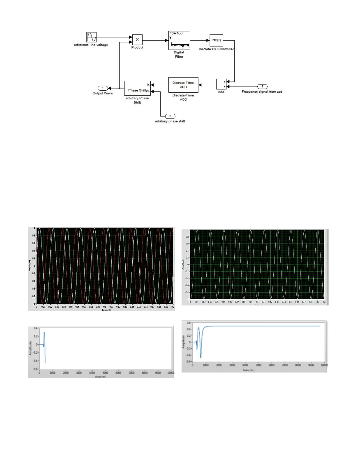
FPGA based Implementation of Frequenc y and Phase Matching T echnique for Grid T ied Applications Uzair Nadeem Department of Electrical Engineering, Colle ge of EME National University of Sciences and T ec hnology (NUST) Rawalpindi, P akistan uzairnadeem92@outlook.com Muhammad Shahzaib Atif Department of Electrical Engineering, Colle ge of EME National University of Sciences and T ec hnology (NUST) Rawalpindi, P akistan shahzaibmsa@gmail.com Rizwan Ahmed Department of Electrical Engineering, Colle ge of EME National University of Sciences and T ec hnology (NUST) Rawalpindi, P akistan rizwanahmed32@ee.ceme.edu.pk Hassan T ouqeer Department of Electrical Engineering, Colle ge of EME National University of Sciences and T ec hnology (NUST) Rawalpindi, P akistan hassantouqeer32@ee.ceme.edu.pk Hamood Ur Rahman Khaw aja Department of Electrical Engineering, Colle ge of EME National University of Sciences and T ec hnology (NUST) Rawalpindi, P akistan hamood@ceme.nust.edu.pk Abstract —A grid tied in verter con v erts DC voltage into A C voltage, while synchronizing it with the supply line phase and frequency . This paper presents an efficient, rob ust, and easy- to-implement grid tie mechanism. First, the grid tie mechanism was simulated in software using LabVIEW and Multisim. Then, the whole system was practically implemented on hardwar e. A prototype hardware was de veloped to produce A C voltage from solar panels. Phase and frequency of the generated voltage were synchr onized with those of a reference sinusoidal signal. The synchronization mechanism was digitally implemented on an FPGA, which also controlled the whole system. W e achieved real time frequency matching with an improved Zero Crossing Detection (ZCD) technique. Phase matching was also achieved in real time using a modified Phase Locked Loop (PLL) algorithm, which r etains stability while being simpler than the general PLL algorithm. Experiments demonstrated that the proposed grid tied system reliably synchronized the phase and frequency of the voltage generated by the implemented hardware with those of the reference grid voltage. Index T erms —Grid Tied Inv erter , Frequency Matching, Phase Matching, Zero Crossing Detection (ZCD), Phase Locked Loop (PLL), FPGA, GPIC (General Purpose Inv erter Controller) I . I N T R O D U C T I O N The ev er increasing energy requirement is one of the biggest challenges faced by the modern world. The depletion of fossil fuels for energy generation is one of the major concerns of the modern age. This has led to a vast exploration of various methods employed for the generation of electricity from renew able sources. The use of solar energy as (virtually) an infinite source of power seems to be the most plausible answer to this situation. Solar panels and photo-voltaic (PV) cells ha ve become the center of attention in this entire scenario. Solar energy can become a viable solution to the problem of energy crisis [1]. Howe ver , there are still many challenges for the ef fectiv e utilization of solar energy . One of the challenges is the efficient con version of Direct Current (DC) electricity harnessed from solar panels to Alternating Current (A C) electricity . Many different in verter designs hav e been proposed so far for the conv ersion of DC to A C [2], [3]. The next major challenge for utilizing solar energy in the national grid is the frequency and phase matching of the generated A C voltage with that of the grid. The implementation of grid tie mechanism on smart local devices is a challenging task [4]. This paper deals with the implementation of frequency and phase matching algorithms on a prototype hardware. The hardware consists of solar panels, a DC-DC con v erter , a full H-bridge in verter , an analog filter , and an FPGA [5]. Output of the solar panels was passed through a DC-DC conv erter , and then fed to a full H-bridge in v erter . Sinusoidal Pulse Width Modulation (SPWM) was used to driv e the in verter circuit [6]. In v erter was followed by an analog filter to produce a sinusoidal output voltage. Phase and frequency of the gener- ated output voltage were synchronized with that of the grid’ s voltage. The synchronization was controlled using the FPGA of the General Purpose Inv erter Controller (GPIC) of National Instruments (NI). Rest of the paper is or ganized as follo ws: Section II dis- cusses the overall mechanism of the grid tied system. Section Fig. 1: A representation of the impro ved Zero Crossing De- tection (ZCD) technique and the hysteresis levels. III describes the simulations and the implementation of the proposed frequency matching technique. Details of the phase matching and PLL (Phase Locked Loop) are presented in Section IV. Finally , the paper is concluded in Section V. I I . D E S C R I P T I O N O F T H E G R I D T I E D O P E R A T I O N In order to grid tie the produced AC voltage, frequency and phase of the generated output voltage are to be matched with those of the grid’ s voltage. W e used Zero Crossing Detection (ZCD) technique to match the frequenc y of the generated signal with the frequency of the A C signal obtained from the national grid. Phase of the generated signal was also matched with the phase of the grid’ s signal using Phase locked Loop (PLL), which was vital in achieving phase synchronization. Both ZCD and PLL were implemented digitally on the FPGA of GPIC. Appropriately scaled feedback from the generated voltage and the grid’ s voltage were used as inputs to the FPGA. Based on the values of these feedback signals, FPGA controlled the SPWM fed to the in verter , which in turn was responsible for performing frequency and phase matching tasks. The disadvantage of using normal square pulse train to operate an H-bridge is that the resulting sinusoidal wav eform contains higher frequency harmonics, ev en after filtration. Therefore, SPWM was used as an input to the in v erter . SPWM greatly reduced the third and higher order harmonics in the output voltage of the in verter . FPGA of GPIC acted as an on- board computer to sense the current A C grid wa veform and produced voltage to correspond with grid. I I I . F R E Q U E N C Y M A T C H I N G Frequency matching is a process in which frequency of the output voltage of the grid tied system is matched with the frequency of the desired signal (grid’ s electricity signal). Encouraging results were obtained for frequency matching using an improved ZCD technique. The following subsections discuss the ZCD technique and its practical implementation. A. Implementation of ZCD T ec hnique As discussed earlier , frequency of the inv erter output should match with the frequency of the reference voltage, i.e., the national grid, in order for the grid tied system to work properly . As a first step of frequency matching, the reference voltage w as fed to the FPGA through an Analog to Digital Con verter (ADC), after scaling it down to the desired level. Input frequenc y was determined by detecting zero crossings using FPGA. Zero crossings are points where sinusoidal signal crosses the zero voltage lev el. After determining the input frequency , an SPWM of the same frequency was generated by the FPGA. This SPWM was then utilized to operate the in verter . B. Impr ovement of ZCD T echnique ZCD technique generally does not perform reliably in noisy en vironment. Hysteresis technique was used to ov ercome this problem. In this technique, zero crossings are detected only on either increasing or decreasing side. In our approach, zero crossings were detected on the increasing side, i.e., while the voltage was going from negativ e to positiv e. FPGA detected frequency by detecting only two zero crossings. Once a zero crossing was detected, two steps were performed in succession to validate it, before detection of another zero crossing. Firstly , voltage lev el must increase above a threshold, called the positiv e hysteresis level. Secondly , v oltage level must decrease below a threshold, called the neg ativ e hysteresis level. Next, zero crossing was detected only after the successful detection of these two steps in succession. Any possible distortion caused by noise in the detection of the grid frequency was eliminated by appropriately determining hysteresis le vel. Fig. 1 shows a representation of the zero crossing detection on the increasing side and the hysteresis levels. Fig. 2: Output screen of oscilloscope for frequency matching at 50 Hz. Fig. 3: Output screen of oscilloscope for frequency matching at 42.88 Hz. C. Softwar e Simulations Before the hardware implementation of the frequency matching, the algorithm was first tested through software simulations. LabVIEW and Multisim softwares were used to test the algorithm with various le vels of noise. Through the improved ZCD technique, the frequency of the generated output voltage was successfully matched with that of the reference voltage. D. Har dwar e T est The nominal frequency of the national grid’ s voltage is 50 Hz. In a grid tied system, grid’ s voltage is the reference voltage whose frequency and phase are to be matched by the system. For testing, we used a sinusoidal signal produced from a function generator as a reference v oltage (in place of the grid’ s voltage). Frequency matching test was then carried out on a number of frequencies, in the range of 35 Hz to 65 Hz. As frequency of the reference v oltage was varied, frequency of the generated output v oltage of grid tied in v erter also v aried accordingly in real time. E. Results of F r equency Matching T ests The frequency matching was reliably achieved during both simulations and hardware implementations. Fig. 2 and Fig. 3 show outputs of the oscilloscope for the frequency matching tests carried out in the lab environment at 50 Hz and 42.88 Hz, respectively . Frequency matching was achieved up to two decimal places. The maximum settling time is two cycles of the reference input wa ve. F or instance, the settling time for a nominal 50 Hz signal is 40 ms. It was not possible to determine the error and precision for more than two decimal places due to the limitation of the testing equipment. Note that the signals are out of phase in Fig. 2 and Fig. 3 as only frequency matching was performed at this stage. I V . P H A S E M A T C H I N G Phase Locked Loop (PLL) is a closed loop control system that generates an output signal whose phase is related to the phase of the input signal. A. Implementation of PLL A PLL consists of a voltage controlled oscillator (VCO), phase detector and a low pass filter [7]. W e implemented PLL digitally (digital phase locked loop) on the FPGA of NI GPIC using LabVIEW . Instead of voltage controller oscillator , a numerically controlled oscillator (NCO) was programmed on FPGA. Phase detector detects and eliminates the phase differ - ences between the reference input signal and the generated voltage. Then, the output signal is again fed to the input and the process continues in real time. PLL loop filter (usually a low pass filter), has two distinct functions. Firstly , its main function is to determine the loop dynamics (stability). This is how the loop responds to distur- bances. Disturbances may inv olve changes in the reference frequency , the feedback divider and the initial mismatch. Secondly , it limits the amount of reference frequency ener gy (ripple) appearing at the output of phase detector , which is applied to the control input of NCO. B. Phase Matching Algorithm Fig. 4 shows implementation of the proposed PLL al- gorithm. This algorithm is simpler and more efficient to implement on FPGA than the standard PLL algorithm. Analog- to-Digital con verters (ADCs) were used to feed the scaled down versions of the generated voltage and the grid voltage to the FPGA. Product of line voltage (reference voltage) and the in verter final output voltage (output wave) was fed to a lo w pass digital filter . Low pass filtering removes high frequency components. Only the DC component, called the error signal, is extracted from the output of the low pass filter for the next stage. A digitally implemented Proportional- Integral-Deri v ativ e (PID) controller was used to impro ve the loop performance. The DC component from the output of the digital filter was fed as the error signal to the PID controller . Output of the PID controller was then added to the frequency measurement signal from the ZCD part (Section III), which was then fed to the NCO (Discrete T ime VCO). Phase shift block in Fig. 4 represents any arbitrary phase shift which may occur due to filter , transformer or load effects. The PID controller was designed to settle the process v ariable to 0.5 on the basis of the following equations: V 1 ∗ V 0 = 1 − cos(4 π f t ) 2 ∗ cos θ + 1 − sin(4 π f t ) 2 ∗ sin θ (1) V 1 ∗ V 0 = cos θ 2 − cos(4 π f t ) 2 ∗ cos θ + sin(4 π f t ) 2 ∗ sin θ (2) where V 1 = sin(2 π f t ), V 0 = sin(2 π f t + θ ) Fig. 4: A block diagram of the proposed digitally implemented Phase Locked Loop (PLL) algorithm. C. Results of Phase Matching T ests Once the phase of the output wav e is matched with the phase of the input wav e, the relative phase difference should be zero. In order to achieve frequency and phase matching, the PID controller attempts to settle the error signal (input process variable) to 0.5 (normalized). 1) Simulations: Before hardware implementation, we per- formed simulations of the proposed PLL algorithm using LabVIEW . Fig. 5 and Fig. 6 show the grid voltage, generated (a) The simulated reference and the generated voltage w av eforms before phase matching (Best viewed in color). (b) Error signal (process variable) to the PID controller at the start of phase matching process (simulation). Fig. 5: W aveforms of grid voltage, generated voltage and the error signal (process variable) to the PID controller at the start of simulations for phase matching. voltage and the error signal (process variable) to the PID controller during simulations. Fig. 5a shows two sinusoidal wa veforms before phase matching. The wa veform with a positiv e cycle first (the one with a lighter shade) represents grid voltage, whereas, the wa veform starting with a negati ve cycle represents the output voltage of the prototype grid tied system. Inv erter output voltage tries to match its phase with that of the grid’ s voltage from the very start. Fig. 5b shows variations in input signal to the PID controller at the start of phase matching. (a) The simulated reference and the generated voltage w av eforms after phase matching (Best viewed in color). (b) Error signal (Process variable) to the PID controller showing phase matching process (simulation). The error signal has settled at the expected value of 0.5 (normalized). See Section IV for detail. Fig. 6: W aveforms of grid voltage, generated voltage and the error signal (process variable) to the PID controller after phase matching has been achiev ed in simulations. Fig. 7: Output screen of oscilloscope showing the reference and the generated wa veforms before phase matching. Fig. 6a sho ws the voltage from the grid and the v oltage from the grid tied inv erter , after phase matching has been achiev ed. The error signal to the PID controller settled at the desired value of 0.5, as sho wn in Fig. 6b. The proposed PLL algorithm took less than one second to achie ve phase synchronization and then tracked the phase of the grid voltage continuously in real time. 2) Har dwar e Results: For hardware testing, we used sinu- soidal voltage signal from a function generator as the reference voltage. Fig. 7 and Fig. 8 show results obtained after practical implementation of phase matching. Fig. 7 sho ws the reference and the generated voltage wav eforms before phase matching, while Fig. 8 sho ws wav eforms after phase matching has been achiev ed. Slight dif ference in wav eforms in Fig. 8 is due to the fact that reference wav eform has no third harmonic (as it is generated from a function generator). Ho we ver , wa veform generated by the grid tied system has a small non-zero third harmonic (as it is the result of an SPWM in verter follo wed by a filter). The grid tied in verter output voltage is always kept slightly higher than the grid’ s voltage, as is also ob vious in Fig. 8. PLL tracked the phase of the reference v oltage and then synchronized the phase of the generated voltage with it. V . C O N C L U S I O N This paper has presented the procedure and results for the simulation and implementation of an efficient and robust mechanism for grid tying a system. W e reliably achieved the main objecti ves of real time frequency and phase matching. W e used Zero Crossing Detection (ZCD) technique for fre- quency matching. Ef fect of noise was canceled with the help of hysteresis levels for an improv ed ZCD implementation. Experiments in the frequency range of 35 Hz to 65 Hz demonstrated that the frequency of the generated voltage was successfully matched with that of the reference voltage up to two decimal places with a maximum settling time equal to Fig. 8: Output screen of oscilloscope showing the reference and the generated wa veforms after phase matching. that of two wa veforms of the reference signal. A modified Phase Locked Loop (PLL) was used for phase matching of the two wav eforms. The PLL was tuned for a set point of 0.5 (normalized). The modified PLL took less than one second start-up time, i.e. to synchronize the phase at start, and then was able to track the phase of the reference wav e in real time. The techniques mentioned in this paper can easily be implemented on an embedded hardware for grid tying purposes. A C K N O W L E D G M E N T This work is partially supported by grant and hardware from National Instruments Corporation NI (Pakistan Office). W e are grateful for their support in carrying out this research work. R E F E R E N C E S [1] Sheikh, Munawar A., ”Energy and renew able energy scenario of Pak- istan, ” Renewable and Sustainable Energy Re views, v ol. 14, no. 1, pp. 354-363, 2010. [2] Dusit Niyato, Ping W ang, ”Cooperative transmission for meter data collection in smart grid, ” IEEE Communications Magazine, vol. 50, no. 4, April 2012. [3] A.Ali Qazalbash, A wais Amin, Abdul Manan, Mahveen Khalid, ”Design and implementation of microcontroller based PWM technique for sine wav e inv erter, ” in IEEE International Conference on Power Engineering, Energy and Electrical Drives (POWERENG’09), 2009, pp. 163-167. [4] Ignacio Lopez-Rodriguez, Mario Hernndez-T ejera, ”Challenges of using smart local devices for the management of the Smart Grid, ” in IEEE International Conference on Smart Grid Communications (SmartGrid- Comm), 2011, pp. 73-77. [5] V ojtch Blahnk, Zdenk Peroutka, Jakub T alla, ”H-bridge power in verter control provide activ e compensation of dead-time effect, ” in 2013 International Conference on Applied Electronics, 2013, pp. 1-4. [6] Nazmul Islam Raju, Md. Shahinur Islam, T ausif Ali, Syed Ashraful Karim, ”Study of SPWM technique & simulation of designed analog circuit (Op-Amp) controlled three phase PWM inv erter with harmonic reduction, ” in 2013 International Conference on Informatics, Electronics and Vision (ICIEV), 2013, pp. 1-6. [7] A. Singhal, C. Madhu, V . Kumar , ”Designs of All Digital Phase Locked Loop, ” in 2014 Recent Advances in Engineering and Computational Sciences (RAECS), 2014, pp. 1-5.
Original Paper
Loading high-quality paper...
Comments & Academic Discussion
Loading comments...
Leave a Comment