A Configurable Memristor-based Finite Impulse Response Filter
There are two main methods to implement FIR filters: software and hardware. In the software method, an FIR filter can be implemented within the processor by programming; it uses too much memory and it is extremely time-consuming while it gives the de…
Authors: Mohammad Hemmati, Vahid Rashtchi, Ahmad Maleki
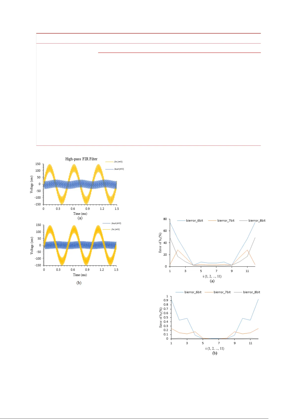
A Configurable Memristor - based Finite Impulse Response Filter Mohammad Hemma ti, Vahid Rashtchi * , Ahmad Ma leki, Siroos Toofan Department of El ectrical Engine ering, University of Zanjan, Z anjan, Iran * Corresponding Author: rashtchi@znu.ac.ir Abstract — There are two m ain methods to imp lement FIR filters: software and hardware. In the softw are method, an FIR filter can be implemented within the pro cessor by programming; it uses too m uch me m ory and it is ex trem ely time-consuming while it gives the design more configurability. In most hardware-based implementations of FIR filters, Analog- to -Digital (A/D) and Digital- to -Analog (D/A) converters are mandatory and increase the cost. The most important advantage of hardware implementation of a FIR filter is its higher speed compared to its software counterpart. In this work, considering the advantages of software and hardware approaches, a method to implement direct form FIR filters using analog components a nd memristors is proposed. Not only the A/D and D/A converters are om itted, but al so using memristors avails con fig urability. A ne w circuit is presented to handle negative coefficie nts of the filter and memristance values are calculated using a heuristic method i n order to achieve a better accuracy in s etting coefficients . Moreover, an appropria te sam ple and delay topology is employed w hich overcomes t he limitations of t he previou s research in i mp le m entation of high-order filters . Proper operation and usefulness of t he proposed structures are al l validated via simulation in Caden ce. Index Terms — M em ristors, FIR filter, Negative coefficients, Sampling circuit, Configurability, Low-pass, High-pass. 1. Introduction After digital signal processors were introduced to the market, their unique features excelled analo g signal processing methods; acco rding to the Mo ore‟ s law , processors become more complex and faster every year . In addition, their programmability giv es the designer m ore flexibility . This trend has made digital signal pro cessors more pop ular and it has led the analog si gnal pro cessing units bec ome rare[1 , 2] . In recent years, i ncreasing speed and reducing size o f transistors have been a challe nge. Thus, scientists ha ve been loo king for any ne w methods t o enhance the perfor mance of processors independent of the so - called trend. One of the approaches is using analog circuits bes ides d igital signa l p rocessing u nits to overco me limitations of digital circuits [3 ]. T his scheme atte mpts to build or enhance digital structures which not only t heir execution within digital pr ocessors consumes too m uch energy , but a lso the y can be i mplemented using pure analo g circuits. Filtering i s an exa mple of such op erations which it is ubiq uitous i n signal pr ocessing applicatio ns a nd it could be a bu rden o n p rocessors. There are various methods to implement filters; pr actical and well - known topo logies ar e Infinite I mpulse Response ( IIR) and Finite I m pulse Response (FIR) [4 ] w hile t his w ork focuses on FIR filters, for they are widely used in s ignal processing ap plications. Structure o f a direct for m FIR filter for m samples is shown in Fig. 1 . are filter co ef ficients; , as the n - th sample, passi ng thr ough each , is delayed for one sampling period. , is the output o f filter which is determined by (1 ). (1) Fig. 1 Direct form F IR filter 1.1 . Evolution of Memristors Memistors were devised in 1960 by W idrow as a 3 - terminal ele ment to be used in adaptive circuits; its resistance was adjustable by one of its terminals which receives DC c urrent [5] . Ho wever , the introduced memistor could not act as the fourth circuit theory element as its I - V characteristic was not fixed and it could only be d etermined within the circ uit which it is used in [6]. Accordingly , in 1968 , Fano and colleagues claimed that except resistor, inductor , and capacito r , there is another missing circ uit element [7 ]. In 1971, an article titled “Memristor - T h e Missing Circuit E lement” pro posing the fo urth 2 - terminal circuit element was p resented by C hua. He believed t hat except three mai n circuit elements ( resistor , capacitor , and inductor), another ele m ent called “memristor” exists which there is a function betwee n it s curr ent flow and its conductance [ 8]. In 2008, researchers in HP lab oratories implemented memristors physicall y [9] which their circuit model for a memristor is shown in Fig . 2. The black co lored end specifies the polarit y of the memristor . I f the c urrent flowing through the me mristor is injected into it via this end, the resistance o f the device is decreased and if the po larity of the c urrent i s reversed, the resistance would b e increased [ 10 ]. Many d ifferent mode ls have been p resented for memristors [ 11 – 18 ]. In this work, the HP model i s utilized . T oday , memristors are used in several applications such as programmable analog cir cuits [ 19 , 20 ], digital cir cuits [ 21 ], 2 accelerators [ 22 , 23 ] , signal p rocessing [ 24 , 25 ], im age processing [ 26 ] , neural net works[ 22 , 27 , 28 ], and etc. Fig. 2 Circuit schema tic of a memristor 1.2 . Background of Memristor-bas ed FIR Filters There are many d ifferent met hods to i mplement FIR filters [ 29 – 32 ], b ut a new ap proach has been prop osed b y [ 33 ] , shown in Fi g. 3. A similar study has also been conducted in [ 34 ] which the results of [ 33 ] have been verified by discrete ele ments instead o f CMOS implementation. In the propo sed structure i n [ 33 ], using a sa mpling circuit with a sampling period of T se co nds, the input is sampled periodically . Using ca scaded samplers, required dela ys are implemented. Instead of resistors which are no t configurable, memristors (as co nfigurable resistors) ar e used to implement co efficients. T hus, the filter can be adapted to any f or m by setting m emristo rs‟ conducta nce to d ifferent values, thus increasing the co nfigurability of filters. T he required addition operation can be implemented b y operational a m plifiers (Op - Amps) i n their small signal region. Fig . 3 The whole FIR filter pr oposed in [ 33 ] The proposed structure in [ 33 ] which is the base of o ur research does not have the capab ility to implement negative coefficients which the y are necessar y in implementing T ype III and T ype IV FIR filters. Moreover, its sampling circuit which is based on Switched–Cap acitor topology has limitations in ac cepting a wide range of input voltages. Furthermore, the OPT D circuit which is responsible for handling delays is not suitable for high ord ers of FIR filters , because of its complexity and inappropriate ca scading technique. 1.3 . Current W ork The purpose of this paper is proposing a novel structure to implement configurable FIR filters usi ng analog cir cuit elements and memristors and d emonstrate its accurac y and proper operatio n. As the main contribution of this work, a new approach for implementing negative coefficients has been p roposed; a heuristic m ethod to reduce the error of implemented coefficients has been applied. Furthermore, using appr opriate circuits as t he sampling blocks, the input range has been increased. T he si m ple dela y units and thei r interconnection scheme have enabled our propo sed structur e to avail higher ord ers of filters co m pared to other works. The rest of this p aper is o rganized as the following. The proposed circuits have been provided in sectio n 2 . Simulations and their results are all covered in section 3 . Section 4 is dedicate d to the conclusion. 2. Main research The p roposed structure for an m th - order mem ristor - based FIR filter is sho wn in Fig. 4. In this sc heme, the input signal is sampled by the track - and - hold unit. Passi ng through delay units, the dela y ed sa m ples ( x[n - m] ) are produced. The scaling b uff ers ( a ) are used to attenuate the input samples i f t heir amplitude is more than the dead - zone of the memristors ( 0.1V specified in [ 34 , 35 ]). Multiplication o f the samples by the co eff icients and adding are done by t he memristors and op - amps, simultaneousl y . Each b lock of the circuit is explained in t he following and the advanta ges of o ur work o ver other implementations ha ve been discussed. Fig. 4 The p r o posed memristor - ba sed FIR filter(dashed ar ea is for handling negative coefficients) 2.1 Handling Nega tive Coefficients As mentioned b efore, the pro posed memristor - based FIR filter in [ 33 ] is onl y suitable for implementi ng specific filters whic h their coefficients are all positive; because memristors could no t get nega tive values. As the main contributio n of this articl e, a new circuit topolo gy (Fig. 5) to handle negative co efficients is proposed . Fig. 5 Han dling negative coefficients Applying circuit analysis fu ndamentals and using ( 1), output of the propo sed structure is determined by (2): (2) 3 where the filter coefficients are described b y ( 3 ): (3) In which and are memristance of memristors for handling positi ve and negative numbers, respectively . In other words, to make a co efficient negative, it is s uff icient that , and vice versa. can be used as a d egree of freedom to assign the ra nge of memristor s. The maximum r esolution o f s etting memristors is ab out 7 to 8 bits [ 34 , 35 ]. In this ca se, the range of memristance would be divided into about 1 28 o r 256 values. T herefore, in setting filter co ef ficients, m emristance values will be set to one of the acceptab le values l imited b y resolution which this will lead to unavoid able discretization errors in coefficients‟ values. T he following met hods are recommended for calculating the value o f memristors in the filter . 2.1.1 . Simple metho d: According to the determined range for m emristance [ 34 , 35 ], for b uilding positive coefficients, should be set to which is the maximum bo undary of memri stance. T herefore the ne gative term of (3) would be minimized. should be chosen in a way that all fall within the deter mined range for memristance. For b uilding negative coefficients, should be set to and the same approach should be applied . It is obviou s that having only one degree of freedo m ( ), it is difficult to set t he c alculated or to the memristance which is limited by reso lution of memristors or tuning circuits. 2.1.2 . Advanced m ethod: In order to decrease the erro r of the calcula ted filter coefficients, values are determined ap plying a heuristic approac h; hence, there are three degrees of freedom which can result to a better accuracy in setting coefficients . The maximum likelihood criteria is used to minimize the following function i n a way that the memristance forming each are selected considering the acceptab le va lues l imited by resolution and giving the minimum F : F= (4) where is the target value (the ideal val ue of the coefficient) and is the erroneous calculated value of the corresponding coefficient (the value which is imple mentable with memristors and suggested b y the heuristic search algorithm). It is worth to me ntion that the op - amp on the final stage is responsible for subtractin g the results o f the first stage op - amps; the va lue o f all the f inal sta ge resistors ha ve b een selected to be eq ual delib erately here to give the unit gain to its inputs. Changing t hese r esistors ( ) can give more degrees of freedom in selecti ng m emri stors‟ values, and also amplification or attenuatio n of the filtered signal. 2.2 . Sampling Circuit Sampler as the first stage of the filterin g operation can be implemented using multiple topologies. The most well - known sa mpling circuit utilizes an N - MOS switch which is illustrated in Fig. 6(a). The on - resistance of the s witch versus i nput volta ge is sho wn in Fig. 6(b ). It is clear that as the i nput voltage be comes bigger, on - resistance of t he switch beco m es worse. This top ology has been used in [ 33 ]. (a) (b) Fig. 6 N-MOS S ampling Circuit (a) N-MOS Switch (b) versus Another app roach is using a P - MOS s witch instead of a N - MOS one in the sa m plin g circuit. This is illustrated i n Fig. 7( a) and its o n resistance ver sus input voltage characteristic is shown in Fig. 7(b). Unlike a N - MOS switch, a P - MOS s witch s hows goo d switching features in high voltages while it ca nnot sa mple t he input correctly for low voltages. (a) (b) Fig. 7 P- MOS sampling circu it (a) P-MOS Switch ( b) versus According to the de ficiency of N - MOS and P - MOS switches, for havin g a larger range of i nput voltage, a boot - strap switch driv ing circuit can be used [ 36 ] to stabilize the Gate - Source voltage of the switch. Using boo t - strap driver increases the over head. Therefore, a co mplementary switch which i ncludes both N - MOS and P - MOS switches in parallel without any boot - strap gate drivers can be used. This structure, called a CMOS switch, is shown in Fig. 8 (a) and its characteristic is s hown i n Fig. 8 (b). Obviously , for a significantly wide ran ge of input voltage, the complementary switch shows a s mooth and approximately linear on - resistance. It has to be mentioned that for driving this s witch, it is nece ssary to have a non - overlapping clock generator to produce clk and clk_b illustrated i n Fig. 4 [ 37 , 38 ] . While overcoming the on - resistance pro blem of the sampling circuit, other side ef fects s uch as clock feed - through [ 39 , 40 ], kT/C noise [ 41 , 42 ], and charge injectio n [ 43 , 44 ]should not be neglected. 4 (a) (b) Fig. 8 CMOS samp ling circuit (a) CMOS S witch (b) vers us In our proposed structure fo r the sampler , in or der to overcome the charge injectio n and the clock feed - through problem, D ummy switches have been used. T he overall sampling circuit is presented in Fig. 9 . Fig. 9 Sa mpling circuit 2.3 . Delay Circuit The designed circuit in [ 33 ] uses cascaded mono - stable circuits for implementing dela y units which it not only req uires e xtra hard w are b ut it also limits the flexibility of the circuits to b e used in high order filters. In ord er to make our design suitable for any order, a Master - Slave topology has been proposed which is sho wn in Fig. 10 . In this circuit, the first stage whi ch receives the input voltage is called the Master, and similarl y the seco nd stage is called the Sla ve. W hen clk becomes low , master s witches will be turned on and the o utput of t he master ( ) will b e almost equal to the input voltage. Du ring low s tate of clk, the sla ve switches re main off . Af ter clk goes to the high s tate, the slave switches will be turned o n and will be mapped to the output. Si milarly , duri ng the high state of clk , master switches re main inactive in ord er not to change the output in the same clock level. Using this struct ure, the control circuit presented in [ 33 ] is o mitted; thus, hardware area is reduced. Clock feed - through is al so handled. It is significant to note that clk and clk_ b must be completel y no n - overlapping; in other words, clk_ b is the logical NOT of clk . Fig. 10 Master - Slave delay unit. 2.4 . Utilized Memristor Model The model for the memristors used in this paper is the HP model [9]. Ordinar y s witching characteristics of this model are shown i n Fi g. 11 , which has been deter mined by sweeping the volta ge across the memristo r in [ 35 ]. T o better illustrate the ran ge of resistors, app roximate numbers for the memristance of the d evice being tested have been presented in Fig. 11 . According to the stability test of the memristor , after it was adjusted to a cer tain value, it retained its value for 50,000 seco nds while being applied a voltage ab out 100 mV . This test was conducted in 350 K degrees and the val ue of the memristor was read once every two seconds. Hence, in this work, if the me mristors are used in ambient temperature a nd it is guaranteed that the value o f the voltage applied to the memristor not exceed 100mV , it w ould be possible for memristors to retain their set values more than ten years [ 35 ]. Fig. 11 S witching characteristics of the memristor [35] The calculated value for and should be adjusted to the memristor by tu ning circuits [ 33 , 44 ]. Having tuning circuits for each memristor can lead to the programmability of the filter for different applications. As mentioned before, it must be noted that a scal ing stage ( a ) is used as a scalar t o keep the voltage applied ac ross the memristor below 100 mV . T his will guarantee that memristors‟ value s for a specific FIR filter will not change by the i nput signal [ 34 ]. 3. Simulation Results and Discussion In this sect ion, the simulatio n results o f the memristor - based filter have bee n presented. All the simulations have been done w ithin the Cadenc e environment. First, the co rrect operation of the sampler unit and delay units has b een investigated. Then, the structure for a low - pass and a high - pass filter is tested and the result s have been illustrated. T o compare the accurac y of the two methods mentioned in section 2.1 , they have been used in d etermining coefficients for 6 , 7 , and 8 bits of resolution i n the simulations. For simplicity , only the o utput sign al for 7 - bit resolu tion has been presented. 3.1 . Samplers and Del ay Unit The sinusoidal signal defined b y (5 ), rep resented in blue in Fi g. 12 , is applied to the circuit shown in Fig. 4. The circuit b eing te sted in this sectio n is a fifth - order filter . is set to 5 p F . The output of the sampler cir cuit is illustrated by 5 black. The other colors rep resent dela yed samples. Fi g. 12 verifies the prop er operation of the delay units. (5) Fig. 12 Th e delayed versions of the input for five orders 3.2 . Implementation of a Low-Pass Filter A low - pass FIR filter with th e properties presented in T able 1 is aimed to be designed. The deter min ed co efficients are calculated u sing MA T LAB FDA T oolb ox. It is to be mentioned that in the majorit y of laborator y implemented memristors there is a n acceptable range for t he ir memristance. For instance, in Fig. 11 , it ca n b e seen that the minimum memristance is 1 b ut its maximum boundary is 1 . Therefore, should be calculated and selected in a way to make sure that and fall in their accep table region. T able 1 Character istics of the lo w - pass filter Order Filter Type 16 Low-pass T o test the d esigned circuit, a signal rep resented by equation (6 ) is app lied to the filter which contai ns two different freq uency co m ponents with eq ual a m plitude s. According to T able 1 , the sampling frequency ( ) is 400 kHz. The cut - frequency ( ) is set to 20 kHz. ( 6) For the designed filter , coefficients have been calculated using both simple and advanced methods based on 6 , 7, and 8 bits of resolution. T o avoid m ass of data, target and calculated values for memristors and coefficients have been presented in T able 2 fo r only 7 - bit reso lution. The perce ntage of error between the target coefficient value and its calculated value is ob tained using equatio n (7). (7) The percentage of error for the coefficients has been calculated and visualized in Fig. 13 for 6 , 7, and 8 bits of resolution. It is clear that the maximum error occurred in setting coefficients for adva nced method is less tha t 1% while it is more than 40% for t he simple method . Fig. 13 Coefficien ts error for low-pa ss filters in 6, 7, and 8 bits of resolution (a) Simple method (b) Advanced m ethod Fig. 14 illustrates t he frequenc y response of the low - pass filter based on simple and advanced method compared to the response of the ideal (original) filter . It demonstrates the high accurac y and us eful ness of th e advanced method in contrast to the simple method for calculation and optimization of the value o f memristors thus coefficients. As an example, Fig. 1 5 shows the output of the circuit for both simple and advanced me thods; the yellow trace (inp ut signal) conta ins 5 kHz and 60 kHz components while, as expected, the o utput is just the shifted version of the lo w - frequency component of . The shift b etween input and output i s the intrinsic c haracteristic of FIR filters. The outputs for bo th simple and advanced methods are similar which this i s the r esult of the fact that t he significant difference b etween t wo methods is mainly i n t wo coefficients which they cannot change the characteristic of the filter considerabl y . Fig. 14 F requency response of the design ed low-pass filter -200 -100 0 100 200 0 0.1 0.2 0.3 0.4 0.5 Voltage (mv) Time (ms) Delay /x[n-2] (mV) /x[n-1] (mV) /x[n] (mV) /out (mV) /in (mV) /x[n-3] (mV) /x[n-4] (mV) 6 Fig. 15 I nput/Output of the low-pa ss filter (a) simple method (b) advanced method 3.3 Implementatio n of a High-P ass Filter Similar to the design p rocess of the lo w - pass filter , a high - pass o ne is desi gned and evaluated to show the feasibility o f ne gative co efficients whic h has been propo sed in this work. The requirements of t he 11 th order filter are shown in T able 3. T he calculated values for the memristors are presented in T able 4 . T able 3. Characteri stics of the high - pass filter . Order Filter Type 11 Highpass The applied signal to the filter is described by equation ( 8 ) which consists of t w o frequenc y co m ponents, 2 kHz and 90 kHz. T o illustrate the oper ation of the filter, the amplit ude of the high - frequenc y co mponent of the i nput signal i s intended to b e much s maller than the lo w - frequency component. The simulatio n result in Fig. 16 shows that the high - frequency co mponent of t he input signal exists in the output and the low - frequency component is totall y filtered. (8) It is al so visible in Fig. 17 that the maximum error for the simple method, like the low - pass filter , is extremely high (about 70% ). In contrast, the error for advanced method is below 1% which s hows the a dvanced method‟ s co m pete ncy over the simple method. T his can also be j ustified using Fig. 16 . In Fig. 16 (a) the low pa ss component‟ s smooth existence is not ig norable in the output while in Fig. 16 (b) the output does not seem to have any considerable lo w - frequency component. S imilar to the lo w - p ass filter in section 3.2, the frequency r esponse of the des igned high - pass filter is sho wn in Fig. 18 which demonstrates that the perfor mance of t he advanced method for calculat ion and opti mization of filter coefficients is slightly better than the simple method. Table 2 V alues o f target and calculated coefficients a nd memristors of the low -pass filter for 7 bit resolution Advanced method ( 𝑹 𝒇 = 48 K 𝛀 ) Simple method ( 𝑹 𝒇 = 136 K 𝛀 ) Target 𝒃 𝒊 Coefficient 𝑹 𝒊 𝑲𝛀 𝑅 𝑖 𝐾 Ω Calculated 𝑏 𝑖 𝑅 𝑖 𝐾 Ω 𝑅 𝑖 𝐾 Ω Calculated 𝑏 𝑖 703 688 0.001543060 1000 984 0.002156537 0.00154566 b0 805 735 0.005681641 1000 953 0.006681507 0.00569446 b1 618 516 0.015224887 1000 891 0.016683004 0.01524095 b2 750 501 0.031811106 1000 805 0.032968697 0.03180934 b3 797 415 0.055341896 1000 703 0.05734059 0.05533191 b4 469 259 0.083064799 1000 618 0.08421784 0.08306805 b5 383 204 0.109803747 1000 547 0.112479831 0.10980299 b6 157 110 0.129297782 1000 508 0.131556061 0.12928842 b7 407 188 0.136423789 1000 493 0.140032665 0.13643644 b8 157 110 0.129297782 1000 508 0.131556061 0.12928842 b9 383 204 0.109803747 1000 547 0.112479831 0.10980299 b10 469 259 0.083064799 1000 618 0.08421784 0.08306805 b11 797 415 0.055341896 1000 703 0.05734059 0.05533191 b12 750 501 0.031811106 1000 805 0.032968697 0.03180934 b13 618 516 0.015224887 1000 891 0.016683004 0.01524095 b14 805 735 0.005681641 1000 953 0.006681507 0.00569446 b15 703 688 0.001543060 1000 984 0.002156537 0.00154566 b16 7 Fig. 16 I nput/Output of the high -pass filter (a) simple method (b) advanced m ethod 4. Conclusion Being a f undamental part of signal p rocessing applications, FIR filters hav e too much cost in ter ms of energy for processor s while t hey can be implemented using analog components. I n this work, a new scheme is pr oposed to implement general purpose configur able mem ristor - based FIR fi lters. A new circuit for handling nega tive filter coefficients is develo ped and tested. In addition, proposing a new tech nique for sampling a nd dela y units, the prob lems of the former research, namel y , b ad sa mpling s witch selecti on , clock feed - through, limited or der of the filter have b een overcome. Finally , to verify the pro poer operation o f the designed circuits, a low - pass and high - pass filter is simulated. T o enhance the accuracy of im pleme nted coefficients, a heuristic method is applied to calcu lating memristors‟ val ues. T he simulations show corr ect oper ation of the proposed structures an d improvement in co eff icients accuracy . The potential future research can be implementing other configurable filters along with app lying ot her heuristi c or nature - inspired optimization algorith ms to calculating memristor values especially in high - order filters to save b oth time and enhance acc uracy . Fig. 17 Coefficien ts’ error for the hig h -pass filter in 6, 7 , and 8 bits of resolu tion (a) Simple method (b) Advanced m ethod Table 4 Values o f target and calculated coefficients a nd memristors of the high -pass filter for 7 bit resolution Advanced method ( 𝑹 𝒇 = 243 K 𝛀 ) Simple method ( 𝑹 𝒇 = 624 K 𝛀 ) Target 𝒃 𝒊 Coefficient 𝑹 𝒊 𝑲𝛀 𝑅 𝑖 𝐾 Ω Calculated 𝑏 𝑖 𝑅 𝑖 𝐾 Ω 𝑅 𝑖 𝐾 Ω Calculated 𝑏 𝑖 750 742 0.003404031 996 1000 -0.002506024 0.00341238 b0 602 586 0.010744041 977 1000 -0.014689867 0.01072902 b1 641 618 0.014369824 945 1000 -0.03631746 0.01438623 b2 696 719 -0.011372795 891 1000 -0.0763367 -0.01139188 b3 344 415 -0.119496585 774 1000 -0.18220155 -0.11947815 b4 282 969 -0.610829511 493 1000 -0.641720081 -0.6108322 b5 969 282 0.610829511 1000 493 0.641720081 0.6108322 b6 415 344 0.119496585 1000 774 0.18220155 0.11947815 b7 719 696 0.011372795 1000 891 0.0763367 0.01139188 b8 618 641 -0.014369824 1000 945 0.03631746 -0.01438623 b9 586 602 -0.010744041 1000 977 0.014689867 -0.01072902 b10 742 750 -0.003404031 1000 996 0.002506024 -0.00341238 b11 8 5. References [1] Rubinoff, M.: “Analog ue vs. Digital Computers - A Comparison” Proc. IRE , 1953, 41, (10), pp. 1254 – 1262. [2] Hahm, M.D., Fried man, E.G., Titlebaum, E.L.: “Analog vs. digital: a co mparison of circuit implementations for lo w- power matched filters,” in “1996 IEEE I nternational Sym posiu m on Circuits and Systems. Circuits and S yste m s Connecti ng the World. ISCAS 96” ( IEEE, no date), pp. 280 – 283 [3] Schlottmann, C.R., Hasler, J .: “High -Le vel Modeling of Analo g Computational Elements for Signal Processing Applicatio ns” IEEE Tran s. Very Large Scale I ntegr. Syst. , 2014, 22, (9), p p. 1945 – 1953. [4] Oppenheim, A. V., Scha fer, R.W., Buck, J .R.: “Discrete - time signal pro cessing” (Prentice Hall, 1999). [5] Widrow, B.: “An Adaptive „Adaline‟ Neuron Using Chemical „Memistor s‟” (1960), pp. 1553 – 2. [6] Hyongsuk Kim, Adhikari, S.P.: “Memistor Is Not Memristor [Express Letters]” IEEE Circuits Syst. Mag. , 2012 , 12, (1), pp. 75 – 78. [7] Fano, R. M. , Chu, L. J ., & Adler, R.B.: “Electromagnetic fields, ener gy, and forces.” (MIT PRESS, 1968 ) [8] Chua, L.: “Memristor -The missing circuit element” IEEE Tran s. Circuit Theory , 1971, 18, (5), pp. 507 – 51 9. [9] Strukov, D.B., Snider, G.S., Stewart, D.R., W illiams, R.S.: “The m issing me mristor found” Nature , 2008, 453, (7191), pp . 80 – 83. [10] Kvatinsky, S., Satat, G., Wald, N., Friedman, E.G., Kolodny, A., Weise r, U.C.: “Memristor -Based Material Implication (IMP LY) Logic: Design Principles and Methodolo gies” IEEE Tran s. Very Large Scale I ntegr. Syst. , 2014, 22, (10), pp. 2054 – 2066. [11] Biolek, Z., Biolek, D., B iolková, V.: “SPICE m odel of memristor with nonli near dopant drift” Radioen gineering , 2009, 18, (2), pp. 210 – 214. [12] Prodromakis, T., Peh, B.P., Papavassiliou, C., Toumazou, C.: “A Versatile Memristor Model W ith Nonlinear Dopant Kinetics” IEEE Tran s. Electron Devices , 2011 , 58, (9), pp. 3099 – 3105. [13] Ya ng, J.J., P ickett, M.D., Li, X., Ohlberg, D.A.A., Stewart, D.R., Willia ms, R.S.: “Memristive switching mechanis m for metal/oxide/metal nanodevices” Nat. Nanotechnol. , 2008, 3, (7), pp. 429 – 433. [14] Lehtonen, E., Laiho, M. : “CNN using memristors for neighborhood co nnections,” in “2010 12 th International Workshop o n Cellular Nanoscale Networks and their Applications (CNNA 2010) ” (IEEE, 2010), pp. 1 – 4 [15] Pickett, M.D., Struko v, D.B., Borghetti, J.L., et al. : “Switching dynamics i n titanium dioxide mem ristive devices” J. Appl. Phys. , 2 009, 106, (7), p. 074508. [16] Abdalla, H., Pickett, M.D. : “SPICE modeling of memristors,” in “2011 IEEE International Symposium of Circuits a nd Systems (ISCAS)” (IEEE, 2011), pp. 183 2 – 1835 [17] Yakopcic, C., T aha, T.M., Subramanya m, G., Pino, R.E., Rogers, S.: “A Me m risto r Device Model” IEEE Electron Device Lett. , 2011, 32, (10), pp. 143 6 – 1438. [18] Kvatinsky, S., Fried man, E.G., Kolodny, A., Weiser, U.C.: “TEAM: T hrEshold Adaptive Memristor Model” IEEE Trans. Circuits Syst. I Reg ul. Pap. , 2013, 60, (1), pp. 2 11 – 221. [19] Sangho Shin, Kyungmin Ki m, Sung -Mo Kang: “Memristor Application s for Programmable Analog ICs” IEEE Trans. Nano technol. , 2 011, 10, (2), pp. 266 – 274. [20] Pershin, Y. V., Di Ventra, M. : “Practical Approach to Programmable Analog Circuits With Fig. 18 F requency response of the design ed high-pa ss filter 9 Memristors” IEEE Trans. Circuits Syst. I Reg ul. Pap. , 2010, 57, (8), pp. 1 857 – 1864. [21] Cong, J., Bingjun Xiao: “mrFPGA: A novel FPG A architecture w ith memristor - based reco nfigu ratio n,” in “2011 IEE E/ACM International S ymposium on Nanoscale Architect ures” (IEEE, 2011), pp. 1 – 8 [22] Nourazar, M., Rashtchi, V., Azarpeyvand, A., Merrikh- Bayat, F.: “Co de Acceleration Using Memristor-Based Appr oximate Matrix Multiplier: Application to Convolutio nal Neural Networks” IEEE Trans. Very Large S cale Integr. Syst. , 2018, pp. 1 – 12. [23] Nourazar, M., Rashtchi, V., Merrikh-Ba yat, F., Azarpeyvand, A.: “T owards memristor -based approximate accelerato r: application to complex - valued FIR filter bank” An alog Integr. Circuits Signal Pro cess. , 2018, 96, (3), pp. 577 – 588. [24] Biolek, D., Bio lkova, V., Kolka, Z.: “Memristive systems for analog sig nal processing,” in “201 4 IEEE International Symposiu m on Circuits and Systems (ISCAS)” (I EEE, 2014), pp. 2588 – 2591. [25] Nourazar, M., Rashtchi, V., Azarpeyvand, A., Merrikh- Bayat, F.: “Me mristor -based ap proximate matrix multiplier” Ana log Integr. Circuits Signal Process. , 2017 , 93, (2), pp. 363 – 373. [26] Hu, X., Duan, S., Wang, L., Liao, X.: “Memristive crossbar array with app lications in image process ing” Sci. China I nf. Sci. , 20 12, 55, (2), pp. 461 – 472. [27] Liu, X., Zeng, Z., Wen, S.: “Im ple mentation of Memristive Neural Net work With Full -Function Pavlov Associative Me mory” IEEE Tran s. Circuits Syst. I Regu l. Pap. , 2016, 63, (9), pp. 1454 – 1463. [28] Li, W., Li, L., Song, J.: “A Ba sic Chemical Synaptic Euler Model and Its T riad Trigger Topology” Chinese J. Electron. , 2 017, 26, (2), pp. 244 – 249. [29] Liu, Y., Parhi, K.K.: “ Lattice FIR digital filter architectures using stochast ic computing,” in “2015 IE EE International Conferenc e on Acoustics, Speech and Signal P rocessing (ICASSP)” (IEEE, 2015), pp. 1027 – 1031 [30] Chen, J., Chang, C. -H., Feng, F., Ding, W., Ding, J.: “Novel Design Alg orith m for Low Complexity Programmable FIR Filters B ased on Extended Do uble Base Number Sys tem” IEEE Tran s. Circuits Syst. I Regu l. Pap. , 2015, 62, (1), pp. 224 – 233. [31] Park, S.Y., Meher, P.K.: “Efficient FPGA and ASIC Realizations of a DA -Based Reconfigurable FIR Digital Filter” IEEE Tran s. Circuits Syst. II Express Briefs , 2014, 61, (7), pp. 511 – 51 5. [32] Gao, Z., Reviriego, P ., Pan, W., et a l. : “Fault tolerant parallel filters based o n error co rrection codes” IEEE Tran s. Very Large Scale I ntegr. Syst. , 2015, 23, (2), pp. 3 84 – 387. [33] Mirebrahimi, S.-N., Me rrikh-Bayat, F.: “Programmable discrete -time type I and type II FIR filter design on the me m ristor crossbar structure” Analog Integr. Circuits Signa l Process. , 2014, 79, (3), pp. 5 29 – 541. [34] Alibart, F., Gao, L., Strukov, D.B.: “A Reconfigurable FIR Filter with Memristo r-Based Weights” arXiv , 20 14, pp. 2273 – 2276. [35] Prezioso, M., Me rrikh-Bayat, F., Hoskins, B.D. , Adam, G.C., Likharev, K.K., Strukov, D.B.: “Training and operatio n of an integrated neuromorphic network based on metal -oxide memristors” Nature , 2015, 521, (7550), pp. 61 – 64. [36] Razavi, B.: “The Boo tstrapped Switch [A Circuit for All Seasons]” IEEE Solid-State Circuits Mag. , 20 15, 7, (3), pp. 12 – 15. [37] Razavi, B.: “Design o f analog CMOS integrated circuits” (McGraw -Hill, 2 004, 2nd ed n.) [38] “Two -phase n on - overlapping clock generator.” US4816700A, 19 87. [39] Weize Xu, Fried man, E.G.: “Clock feedthrough in CMOS analog transmissio n gate switches,” in “15th Annual IEEE International ASIC/SOC Conference” (IEEE, no date), p p. 181 – 185 [40] Minkyu Song, Yongman Lee, Wonchan Kim: “A clock feedthrough reductio n circuit for switched - current systems” IEEE J. Solid-Sta te Circuits , 1993, 28, (2), pp. 133 – 137. [41] Fischer, J.H.: “Noise sources and calculation techniques for switched ca pacitor filters” IE EE J. Solid-S tate Circuits , 1982, 17, (4), pp. 742 – 752. [42] Baker, R.J.: “CMOS: Circ uit Design, Layout, and Simulation, Third Edition. Wiley- IEEE” ( John Wiley & Sons, 2010 ) [43] Wegmann, G., Vittoz, E. A., Rahali, F.: “Charge injection in analog MOS s witches” IEEE J. S olid- State Circuits , 198 7, 22, (6), pp. 1091 – 1097. [44] Berdan, R., P rodrom akis, T ., Toumazou, C.: “High precision analogue me mristor state tuning” E lectron. Lett. , 2012 , 48, (18), pp. 1105 – 1107. 10 Moha mm ad Hemmati received his B .Sc and M. Sc degree from University Of Zanjan, Zanjan, Iran in Electrical and Electr onics Engineering, in 201 3 and 2016 , respectively . He was a visitin g lecturer at Electrical E ngineering department at Universit y o f Zanjan, tea ching Digital Desig n and Micropro cessors Laboratories for m or e than two years. He is currentl y working as an e mbedded systems d esigner and CEO at Ofogh Sanaat P aydar Za ngan doing research on bio medical signal processing, embed ded systems, and computer visio n. His research interests inc lude Embedded Systems , FPG A - based Digital Design, Geo metry of V ision, Fault - T olerant Syste ms , and Artificial Intelligence in Biomedical applicatio ns.(Email: m_he mmati@znu.ac.ir ) V ahid Ra shtchi was born in 1967 in Zan jan, Iran. He receive d his B.Sc. in electr ical e ngineering from T abriz University in 1991 and his M.Sc. and Ph.D. in electrical engineering from Am irkabir University of T echnology , T ehran, Iran, in 1993 and 2001 , respectively . He is currently working as an as sociate p rofessor at University o f Zanjan, working on power electronics and ap plications of artificial intelli gent systems since 2001 . Up to now , he has had several positions such as "Hea d of the E ngineering Faculty", " Research V ice Chancellor" at University of Zanjan and “Chairman of the National Elites Foundation - Zanjan Branch”. (Email: rashtchi@znu.ac.ir ) Ahmad M aleki (Non - member) was born in 1992 in Loresta n, Iran. He received his B.Sc. in electrical engineering from Ur mia University , Urmia, I ran, in 2014 . He holds a Masters in Electronics from University o f Za njan, Za njan, I ran doing research on Me mristors and their applications. His research in terests include FP GA - based Desig n, signal processing, and image processing. (Email: maleki.a@znu.ac.ir ) Siroos T oofan (Non - member) received the B.Sc. degree in Electronics Engineering from Amirkabir University of T echnology (T ehran Pol ytechnic) in 1999 , and the MSc. And P hD degree in Electronics Engineer ing form Ir an University of Science and T echnology (IUST) in 2002 and 2008 , respectively . During 2007 to 2008, on his sab batical leave, he was with the VLSI group of Po litechnico di T or ino and in the Microelectronics - Integrated Circuits Lab. o f t he P olitechnico di Mila no in Italy . He has been working as an assistant professor with t he Department of Electrical En gineering, Universit y of Zanjan, since 2009 . His current r esearch activities i nclude the design of CMOS Analog I ntegrated Circuits, RF I ntegrated Circ uits and Capacitive Sensors Readout Circuits. (Email: s.toofan@znu.ac.ir )
Original Paper
Loading high-quality paper...
Comments & Academic Discussion
Loading comments...
Leave a Comment