Artificial Retina Using A Hybrid Neural Network With Spatial Transform Capability
This paper covers the design and programming of a hybrid (digital/analog) neural network to function as an artificial retina with the ability to perform a spatial discrete cosine transform. We describe the structure of the circuit, which uses an anal…
Authors: Richard Wood, Alex, er McGlashan
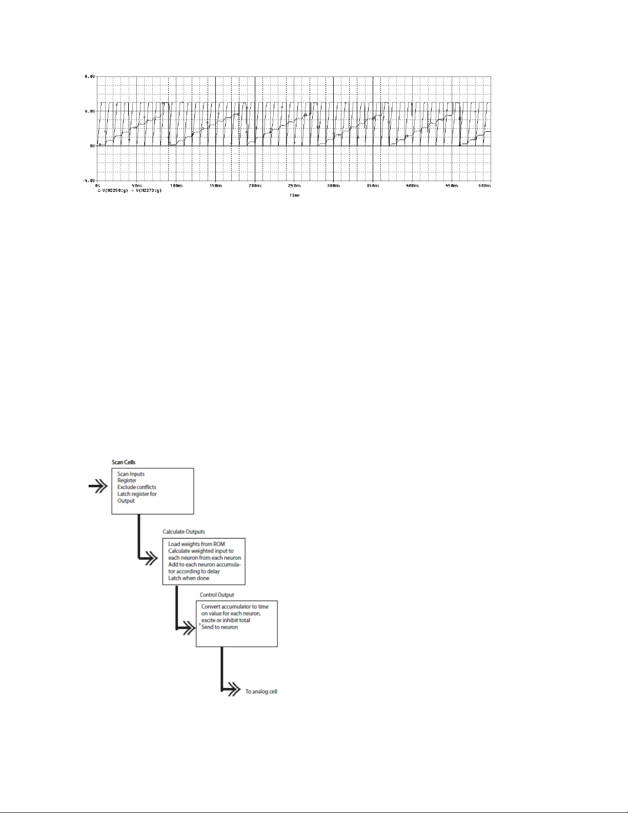
Artificial Retina Using A Hybrid Neural Network With Spatial Transform Capabil ity Richard Wood Honeywell, Inc., Sp ace Payloads Ontario, Canada Alexander McGl ashan Niagara College Welland, Ontario C.B. Moon Hoseo University South Korea W.Y.Kim Hoseo University South Korea Abstract — This paper covers the d esign and programm ing of a hybrid (digital/analog) n eural network to function as an artificial retina with the ab ility to perform a spatial discrete cosine transform . We describe the struc ture of the circuit, which uses an analog cell that is interlinked using a programmable digital array. The paper is broken into three ma in parts. First, w e present the results of a Matlab si mulation. Then w e show the circuit simulation in Spice. T his is follow ed by a demonstration of the practical device. This syste m has int entionally separated components w ith the specialty analog circuits being separated from the readily available digital field programmable gate array (FP GA) components. Further development includes the use of rapid manufacture-able organic electronics used for t he analog componen ts. T he planned uses for this platfor m include crowd development of softw are that uses the un derlying pulse based p rocessing. The development package will include sim ulators in the form of Matlab and Spice type softw are platforms. Keywords-Analog Neuron, FPGA Neuron, Neural Spatial Transfor m ; I. I NTRODUCTI ON This paper covers the design an d programm ing of a hy brid (digital/ analog) neural network to function as an artifici al retina with the ability to perform a spatial discrete cosine transform . We describe the struc ture of the circuit, which uses an analog cell that is interlinke d using a programm able digital array . The paper is broken into three main parts. First, w e pres ent the results of a Ma tlab simu lation. T hen we show the circuit simulation in Spice. T his is follow ed by a demons tration of the practical device. T his sys tem has intenti onally separated components with the specialty analog circuits being separated from the readi ly available digital fiel d programm able gate array (FPGA) components . Further developm ent includes the use of rapid manufactu re-able organic electroni cs used for the analog components . The p lanned uses for this platf orm inclu de crow d dev elopment of softw are th at uses the unde rlyin g pulse based processing. T he development package will inclu de sim ulators in the form of Matla b and Spic e type sof tware platform s. II. B ACKGRO UND There are a num ber of hybrid neural network designs in developmen t 1-80 . These include Spinnaker, T rue north. Neurogrid , and Brainscales. Spinnake r and True North use an Address Event Representat ion (AER). In Neurogri d, analog neural effects are modelled and sy naptic paths are shared. T he current sy stem uses an approach in w hich all synaptic connecti ons exist at a ll tim es in a high spee d seria l archite cture. The d iscrete cosine spatia l transf orm can be used for textur e analysis . T he vari ations in texture in objects can be used to d etermin e relative distance as well as defining the structure itself. These cosine transforms demons trate one aspect of the circuit . By definition, any function is programm able including complex func tions. T he circuit can also be dy namically reprogram med for differen t fun ctions wh ile in ope ration . III. B ASI C D EVICE D ESCRIPTION The follow ing is an overview of the hy brid (analog-digi tal) d esign of the neural processor. T here are two main points to note. 1. T he design involves the use of analog neural netw ork cells that are interlin ked using an integrate d digital interfac e. 2. T he base design described here is an 8x8x 3 layer hybrid neural net, specific ally designed for use as a textu re analy zing ci rcuit based on a dis crete cosin e tr ansform algorith m. The cells can be programm ed through a scann ing array via the digital interface. The digital int erface in this implem entation is compos ed of an FPGA which has be design ed in two main configura tions. One w ith a high level of parallel processin g and the other in a high speed serial configu ration. T he analog cells are monit ored through a scanning array and the inform ation is then digitize d and stor ed in the FPGA . The scannin g occurs at least 1000 times the rate of pulses (MHz versus kHz) . T he scanned cell inform ation is then stored in a register . T his register is used to calculat e the total excite or inh ibit syn aptic input for each cell of the next lay er. The input cell register is scanned and the weighted effect for each syn aptic connection is stored in an accum ulator for the design ated receptor cell in the next layer. These accumu lators are structured accordin g to d elay (complex weight) so that they are stored in an accumu lator that is u sed during a fu ture cycle. The weights can be dynamically updated to change the system interlink ing co nfigur ation. The inform ation is then converte d into r esultan t “ ti me - on ” information to be passed to the connected synapse . The resultant “time - on ” will be either inhibito ry or excitato ry. When the individual cell has b een on lo ng enough the input current will be turned off. This sy stem works on the premise that the average ce ll input current based on total o n time is equivalent to the summation of input inhibitory and excitatory pulses. It is time scale dependent . The current configu ration uses pulse rate info rmati on for p rocessin g. An arriv al time sy stem is possible within the scannin g an d process ing tim e limits imposed by th e system . In the example of the 8 x8x3 layer system , the first layer is an array of detector cells, converting light int ensity into an array of pulse rates. T his is then subject to a 1D row discrete cosine transform , with the inform ation still expressed as pulse fre quencies . This second 8x8 array is then also subject to a 1D transfo rm (along the colum ns). The result is a 2D cosine tr ansfo rm encode d as varia ble rate pulse s. The tr ansfo rm is a dir ect r esult of the st ored w eights . Figu re 1 shows an illustrati on of th e 8x8x3 layer neura l netw ork system . Each circl e repre sents an analog pulsing integratin g cell. These cells are int erconn ected via a rast er system an d bus lin es that feed into the F PGA and processor , as in Figure 2. The first layer is continuously scanned for output p ulses. When a pulse is detected, it is stored in a transien t look-up table tabulate d b y source location. T here are 6 4 indivi dual source locations in the firs t layer. These are then converted into a follow ing table by multiplying by stored weight values and accumu lating according to destination cell and time delays. The delay size and resoluti on can be altered as required. This inform ation is then encoded into a total time on for the destination cell (either an inhibitor y or excitato ry connection). This effectiv ely m eans that although each cell in layer 2 has 128 synaptic input conn ections and 128 output connecti ons, there is only o ne each of inhibit and excite p hy sical connections fo r a total of 4 connecti ons per cell. There are 128 virtu al inhibit and excite synapses in the digital domain. T he analog cells can also be programm ed (thresho ld voltage , refra ctory tim e, etc.) via the integ rated in terfa ce. Figure 1. Syste m Overview Figure 2. Sample of A rray Figu re 3 shows a sample of the neuromorphic analog cell. Figure 4 show a typical mem brane potential of the analog cell . Figure 3. Analog Neuromorphic cel l. Figure 4. Typical Mem brane Potential of Neuromo rphic cel l. Figu re 5 shows the scanning array of neuromorphic cells. At high speed, the analog cells are scanned for pulses. The scan time is orders of m agnitude less than th e m aximum pulse rate. Figure 5. Scanning Ar ray of Neuromorphic cells. Figu re 6 and 7 illustr ate the w eight calculat ion. Each of the neurons in the first layer is connecte d to every cell in the following layer by a given weig ht wh ich includes a time delay (complex connection ). A destination-delay table is used to store and accumulate these weighted results. For exam ple, if neuron A, B , C and D fired, they are then connected to neuron 1 in the next layer. B ut, we assum e that the weight fun ction between C and 1 has a delay different than A, B and D. In this case, the weighted results of A, B and D are accumulate d and stored in one column of the table and the weighted result of C is stored in a delaye d column for neuron 1. This table is constantly upgrade d and shifted accordin g to the tim e delay. The resolution and r ange of the time delay determin es the size of the table. Since the w eights can be eithe r excitat ory or inhi bitory , the re sultant totals are eith er one or t he othe r as w ell. Figure 6. Weight Calc ulation. Figure 7. Destination-De lay Table . Figu re 8 shows the syn aptic stimulating scanning array. T he data in the destination- delay table, in column 1 , is no w interpreted as resultant “tim e -on ” (either inhibit or excite). T he array show n is scanned by column, any neurons in that column that have a total current on value are simulta neously turned on (excite or inhibit). T he next column is then scanned. Once all columns are scanne d, the system goes back to the first and turns off any neuron currents t hat have reached their total “on -tim e ” value. T he system effectively digitally integrates pulse trains over short periods of time and converts them into total current v alues f or tha t short tim e period as show n in f igure 9. Figure 8. Scanning input p ulse array . Figure 9. Pulse-T ime Conversio n IV. D I SCRETE C OSIN E T RANSFORM For an 8- by -8 m atrix of neu ral cel ls, T*A is an 8- by -8 m atrix whose c olumn s contain the one-dim ensional DC T of the colum ns of neural cell matrix A. The two-dim ensional DCT of the neur al matrix A can be com puted as B=T*A*T', with B being th e output m atrix and T and T' a re th e weig ht matrix and its t ransp ose. V. D ISCUS SION A. Matla b simulation In Matlab we designed the simulation as per the system illustrate d in Figure 1. The simu lation uses an analog cell approach with a runge kutta so lution . T he weights are pro gramm ed d iscretely . The inputs to the first layer are simu lated as relative light inten sity. Figure 10A il lustrat es the input 8 x 8 array , showing the layer output of a single sample test pattern. Figure 1 0B illu strat es the hidden 8 x 8 array layer that performs the first o ne dimensional DCT. Figure 1 0C illustrates the 8 x 8 o utput array layer that p erfo rms the second one dimension al DCT. A complete series of test patterns w as evaluated . Figure 10. A) Input L ayer Pulse Graph B) Hidden L ayer Pulse Graph C) O utput L ayer Pulse G raph B. S pice Simulation The follow ing section gives a high level overview of the Spice simulation . T he system comprises a grid o f neural cells as show n in Figur e 11, with a represen tative individual cell shown in Figure 1 2. The contr ol circuit (FPGA) is implem ented digitally (not shown). Figure 13 illustrat es the representat ive integrate d input to a single neu ron with the neurons m embrane potenti al. Figure 11. Neural A rray (Selection 3 x 3) Figure 12. Basic Cell Figure 13. Representative pulsing input of a singl e neuron. C. Practical Device. The practical device was implem ented in two forms. 1. A hy brid device with the co ntr ol circuitry designed in an Altera FPGA, w ith the digital process or combined w ith external analog circuits (neu ral cells), in a scanning matrix. 2. A system in which the entire design is implem ented in an Altera FPGA with the analog neural cells and the scanning array em ulated w ithin the FPGA . 1) Hybrid Implemen tation Figure 14 illust rates the functional schematic of the hybrid system. This design was implem ented in two versions, a parallel and a serial configurat ion. T he prim ary differen ce being that in the parallel version, each destinat ion cell calculat ion is d one in paralle l, requ iring 64 separ ate cir cuits. Referring to Figure 14, the calcul ate outputs block defin es the time sequencing. T he weights are loaded from RAM. The accumu lator for each destination neural cell is updated in sequence as each of the 64 input cells firing register is scanned for activity and the designate d weig ht is added to the accum ulator of the destinati on cell . T hese calculat ions result in a r equir emen t for 4096 cycles to calculate all the output amoun ts in the serial versi on and 64 cycles in the par allel version . In this exam ple, that resul ts in a 82 us cy cle tim e for the s erial version. Figure 14. Functional Schema tic of the sy stem with exte rnal analog neuro n. Table 1 illustra tes the FPGA resource usage for the design with an external analog neural cell. Shown ar e the tw o versions, one with the implementation using mostly logical elements in p arall e l and a serial version using mostly on- chip RAM. In either case, the r esource usage will scale as the square of the number of neur ons. In the case of the latter im plemen tation, th e logi cal el ement u sage is 3 per neu ron. Figure 15 show s the chip resource us age for the se rial ve rsion with the external anal og neu ral cel l. Figure 15. Chip Usage, Ser ial Version w ith External A nalog Neural Cell. 2) Full FPGA Imp lementation Figure 16 illustrates the functi onal schem atic of the system in which the entire design is implem ented in an Altera FPGA with the anal og neu ral c ells and th e scan ning a rray em ulated w ithin th e FPGA. Tab le 1 . FPG A w i th E x t ern al A na log C ell Paral lel V ers i on Seri al V e rs ion Fl o w S t at u s Succ es s ful - Tue Mar 2 7 2 0: 13 :1 5 20 1 8 Fl o w S t at u s Succ es s ful - Thu A p r 0 5 1 8: 23 :4 2 2 0 1 8 Quartu s II 64 -B it V ers ion 1 3 .0 .0 Buil d 1 56 04 / 2 4 /20 13 S J Web E d iti o n Quartu s II 64 -B it V ers ion 1 3 .0 .0 Buil d 1 56 04 / 2 4 /20 13 S J Web E d iti o n R e v i s ion N am e DE 2 _ D5 M R e v i s ion N am e DE 2 _ D5 M To p-l ev el E n tity N am e Neural Network 2 To p-l ev el E n tity N am e Neural Network 2 Fam i ly C y c l on e I I Fam i ly Cyclon e II Device E P2 C3 5F6 72 C6 Device E P2 C3 5F6 72 C6 Ti m i n g Mo d e l s Fi n al Ti m i n g Mo d e l s Fi n al To ta l l o g i c el em en t s 5 ,9 10 / 3 3,2 16 ( 18 % ) To ta l l o g i c el em en t s 5 7 5 / 3 3,2 16 ( 2 % ) To ta l com b inat iona l f un c tion s 5 ,5 88 / 3 3,2 16 ( 17 % ) To ta l com b inat iona l f un c tion s 5 3 5 / 3 3,2 16 ( 2 % ) Dedicate d l o g ic regis te rs 3 ,2 44 / 3 3,2 16 ( 10 % ) Dedicate d l o g ic regis te rs 3 0 5 / 3 3,2 16 ( < 1 % ) To ta l r e g i s t ers 3244 To ta l r e g i s t ers 305 To ta l pi n s 2 5 8 / 4 75 ( 5 4 % ) To ta l pi n s 2 5 8 / 4 75 ( 5 4 % ) To ta l vi rtu al p ins 0 To ta l vi rtu al p ins 0 To ta l m e m o ry bits 4 9 ,1 52 / 4 83 ,84 0 ( 10 % ) To ta l m e m o ry bits 3 5 ,8 40 / 4 83 ,84 0 ( 7 % ) E m b ed d ed Mu ltipl ier 9 -bi t elem ent s 0 / 7 0 ( 0 % ) E m b ed d ed Mu ltipl ier 9 -bi t elem ent s 0 / 7 0 ( 0 % ) To ta l P L L s 0 / 4 ( 0 % ) To t al PL L s 0 / 4 ( 0 % ) Figure 16. Implementation w i th Neural Cel l Emulated in The F PGA. Table 2 illustrates the FPGA resource usag e for the design with the neural cell emulated within the FPGA. Show n are two versions, one with the implem entation using mostly logical elements in parallel and a serial implem entation using mostly o n chip RAM. Co mparing to the vers ion with the external analog neural cell, the neuron requires 9 logical elements to emulate each neuron. As resources other than the neural cell scale by the square of the number o f neurons and the cell resource usage scales lin early with the nu mber o f neur ons, the resour ce usage ad vantage o f one implem entation over the other is design s p ecifi c. Figure 17 show s the chip resource usage f or the s erial versio n w ith the exte rnal an alog neu ral cell. Tab le 2 . FPG A w i t h E m u l a t ed N eu ral Cel ls. Paral lel V ers i on Seri al V e rs ion Fl o w S t at u s Su cce s s ful - Th u Mar 2 9 1 7: 41 :4 3 20 1 8 Fl o w S t at u s Succ es s ful - Sat Ap r 0 7 0 9: 21 :0 0 2 0 1 8 Quartu s II 64 -B it V ers ion 1 3 .0 .0 Buil d 1 56 04 / 2 4 /20 13 S J Web E d iti o n Quartu s II 64 -B it V ers ion 1 3 .0 .0 Buil d 1 56 04 / 2 4 /20 13 S J Web E d iti o n R e v i s ion N am e DE 2_D5 M R e v i s ion N am e DE 2 _ D5 M To p-l ev el E n tity N am e Neural Network 2 Top -l e v el E nt ity N a m e Neural Network 2 Fam i ly C y c l on e I I Fam i ly C y c l on e I I Device E P2 C3 5F6 72 C6 Device E P2 C3 5F 6 7 2 C 6 Ti m i n g Mo d e l s Final Ti m i n g Mo d e l s Fi n al To ta l l o g i c el em en t s 1 1 ,1 55 / 3 3,2 16 ( 34 % ) Tot al l o g ic el e m en t s 1 ,0 43 / 3 3,2 16 ( 3 % ) To ta l com b inat iona l f un c tion s 1 0 ,7 99 / 3 3,2 16 ( 33 % ) Tot al co m b i na tion al f u n ct ion s 9 9 3 / 3 3,2 16 ( 3 % ) Dedicate d l o g ic regis te rs 4, 58 4 / 3 3,2 16 ( 14 % ) Ded i cat ed l og ic r e g i s t ers 42 7 / 3 3,2 16 ( 1 % ) To ta l r e g i s t ers 4584 Tota l reg ist e rs 427 To ta l pi n s 2 5 8 / 4 75 ( 5 4 % ) To t al pi ns 2 5 8 / 4 75 ( 5 4 % ) To ta l vi rtu al p ins 0 To t a l v ir t u al pins 0 To ta l m e m o ry bits 4 9,1 52 / 4 8 3 ,8 40 ( 1 0 % ) To ta l m e m o ry bits 35 ,9 68 / 4 83 ,84 0 ( 7 % ) E m b ed d ed Mu ltipl ier 9 -bi t elem ent s 6 4 / 7 0 ( 91 % ) E m b ed d ed Mu ltipl ier 9 -bi t elem ent s 0 / 7 0 ( 0 % ) To ta l P L L s 0 / 4 ( 0 % ) To ta l P L L s 0 / 4 ( 0 % ) Figure 17. Chip Usage, Ser ial Version w ith Emulate d Neural Cell. VI. R ESUL TS A. Timing issues with time sequ enced syna pses. Timing error results from the convers ion of pulses into time on/off o f the synapses . W ith the present serial implem entation, there is an approxim ate 82 us requirement for the calculation o f the weighted sum s of synaptic inputs. This then defin es a scan period of 82 us. A staggere d system is possible but the com plications were deemed to be unnecessa r y. This results in a total possible delay of between 82 and 246 us. In the worst case scenario, a pulse begins at the beginning of a cycle and then the current is on until the end of a cycle (maxim um s ynaptic connecti on) . Figure 18 show s the time spr ead of d elay s in a Monte Carlo s imu lation of 100 00 input pattern variati ons. Figure 18. Time Spre ad Of Delays I n A Monte Carlo Simulation Of 1000 0 Input Patte rn Variations The d ecay function for the analog cell is on the order of 10%/ ms. The delay will cause an error of less than or equal to 0.1%. T his is well below the accuracy of the pulse train system . The quantiza tion of the delay periods also creates an error . B. S tability Analysis of Dig ital-Analo g Domain. A b asic phase state analysis follow s . Figure 19 compares the quantized (dots) and non- quantize d (solid line) synaptic pulses, in term s o f the p hase stat e. A sam p le of th e q uantized in put is show n in Fig ure 13. Figure 19. Phase Analy sis. C. Learning (Digital) Learning is mostly in the d igital dom ain with some p rogramm able features available in the analog implem entation . T he circuit can use numerous learning algorithm s as it is external to the implementation . T he time sequencing and p ulse activity is available within the system for further enhanced learni ng that may include arrival time. A normalized hebbian algorithm has been implem ented, although the DCT configu ration is conside red hard - wired. D. Accu racy In biological optical neural ac tivity there are firing rates up to 250 to 1000 Hz with averages in the 9 to 18 Hz. Using a nom inal 10 Hz firing rate, if we encode o nly with pulse rate of a single neural train, we have a maxim um accuracy of 10% (using a 1 second evaluati on perio d). In a practical device, we have the option of adding m ore neurons in parallel to split the input and increase the accuracy. In a practical system , this would also reduce th e effect of lost neurons. Other encoding options are possible such as the use of a power sca le (logarithmic) . For the present example of a spatial frequency decoder, a 10% accuracy is sufficient. I f using p ulse timing, the accuracy is limited to the scanning time period, 82 us giving a nominal accu racy o f 0 .0008% . In the context of sac cades, the frequency component o f the im age (spatial tran sform) is technic ally in dependen t from the eff ect of im age jitter. E. Po wer Consumption A detaile d analy sis o f comparative power consum ption is beyond the scope o f the present work. Howev er, the analog hy br id vers io n us es sign ificantly less com ponents in t he integrator. F. Noise Noise scal es line arly w ithin the sy stem. No ise of spatial fre quencies that are me asured b y the system will be passed through to the output layer, Figure 20 . Implementin g a recurrent neural netw or k will allow for tem poral noise filtering . Figure 20. Noise. G. Accessible To ol for Studen ts, rapid proto typing, application specific. Goal is t o m ake an accessi ble tool. The digit al-analog design sim plifies rapid pr ototypin g. VII. C ONCLUSI ON S This work has outlined the design, implemen tation and testing of a pulsin g hybrid neural circuit using an Altera FPGA in co njunc tion with an external analog neural cell matrix. A n all FPGA version has also b een developed as a point of c omparison. T he delay and accuracy reducti o n due t o quantizati o n has b een foun d to be bel ow th e acceptance threshol d . The phase sta bility is unaffected by the quantizati o n. Future work includes the d evelopm ent of abstra ction layers f o r cont rol of th e syste m as well as im plementation i n an organic el ectronics matrix. VIII. R EFERENCES [1] Tunable device-mismatch effects for stochastic computation i n analog/dig ital neuromorphic c omputing a rchitectures R ichard George and Giacomo I n diveri . 2016 I EEE International Confe rence on El ectronics, Circuits and Sy stems (ICECS) [2] Training Itself: Mixed-signal Training Acceleration for Memristor-based Neural Network Boxun Li, Yuzhi Wang, Yu Wang, Yira n Chen, Huazhong Yang , Dept. of E.E., TN List, Tsinghua Univ ersity, Beijing, C hina. De sign Automation Confe rence (A SP -DAC), 2014 19th A si a and South Pacifi c [3] Device and System Level Design Considerations for Analog-Non-Volatile-Memo ry Based Neuromorphic Architectures S. Burc Eryilmaz, Duygu K u zum, Shimeng Yu, H.-S. P hilip Wong. 20 15 I EEE International Ele ctron Devices Mee t ing (IED M) [4] Precise deep neural n etwo rk computation on imprecise low-power analog hardware Jonathan Binas, Daniel Neil, Giacomo Indiveri, Shih - Chii Liu, Michae l Pfeiffe r. 2016. arXiv preprint arXiv:1606. 07786 [5] Backpropagatio n fo r Energy-Efficient Neuromorphic Computing. Steve K . EsserRathina kumar Appuswamy Paul A . Merolla Joh n V . Arthur Dharme n dra S. Modha. A d vances in Ne ural Infor mation Processing Syste ms 28 (NIPS 2015) [6] A 3.43TOPS/W 48.9pJ/Pixel 50.1nJ/Classificat ion 512 Analog Neuron Sparse Coding Neural Netwo rk with On -Chip Learning and Classification in 40nm CMOS Fred N. B uhler, Peter Brown, Jiabo Li, Thomas C hen, Z hengya Zhang and Michae l P. F lynn 2017 Symposium on VL S I Circuits Digest of Te chnical Papers [7] RENO: A High-efficient Reco nfigurable Neuromorphic Computing Accelerator Design Design Xiaoxiao L iu, Mengjie Mao, Beiye Liu, Hai Li, Yiran Chen . Design Autom a tion Co nference ( DAC), 2015 52nd A C M/EDA C /IEEE [8] Milde M B, Blum H, Dietmülle r A, Sumi slawska D, Conradt J, Indiveri G and Sandamirs kaya Y (2017) Obstacle Avoidance and Target Acquisition for Robot Navigation Using a Mixed Signal Analog/Digital Neuromor phic Processing System. Front. Neuroro bot. 11:28 . d oi: 10.3389/fnbot.2 017.00028 [9] Qiao N,Mostafa H, Corradi F, O ssw ald M,Stefa n ini F,Sumislaw sk a D andI n diveri G(2015)A reco nfigurable on-line learning spiking neuromorphic pro cessor compris ing 256 neuro n sand128Ksy nap ses. Fro nt. Neurosci.9:141. doi: 10.3389/fn ins.2015.00141 [10] A h ybrid analog/digital Spike-Timing Dependent Plasticity learning circuit for neuromorphic VLSI multi -neuron archit ectures Hesha m Mostafa, Fe derico Corradi, F abio Stefanini, an d Giacomo I nd iveri. 2014. [11] Filippo Grassia, Timothée Levi, E Doukkali, T Ko hno. Spike pattern reco gnition using artificial neuron and Spike -Timing-Depe ndent Plasticity imple mented on a multi-core embedded p latform. 22th I nternational Symposium on Artificial Life and Robotics, Jan 2017, Beppu, Japan. 2 2th I nternational Sympo sium on Artificial L ife and Robotics. [12] Delay-Based Reservoir Computing: Noise Effects in a Combined Analog and Digital Implementation Article i n I EEE Transactions on Neural Netwo rks and Learning Systems · February 2015. Miguel C. Soriano, Member, I EEE, Silvia O rtín, Lars Keuninckx, Lenner t Appeltant, Jan Da nckaert, Member, IEEE, L ui s Pesquer a, and Guy Van der Sande [13] E. Ch icca, F. Stefanini, C. Bartolozzi, and G. I nd iveri, “Neuromo rphic electronic circuits for building autonomous cognitive system s,” Procee dings of the IEEE, vo l. 102, no. 9, pp. 1367 – 1388, Sep 201 4. [14] P. A. Merolla, J. V. Arthur, R. Alv arez- Icaz a, A. S. C assidy, J. Sawada, F. Akopyan, B. L. Jackson, N. Imam, C. Guo, Y. Nakam ura, B. Brezzo, I. Vo, S. K. Esser, R. Appusw amy, B. Taba, A . Amir, M . D. Flickner, W. P. Risk, R. Manohar, and D. S. Modha, “A million spiking- neuron integrated circuit with a scalable communication network and interface,” Science, vol. 345, no. 6197, pp. 668 – 673, Aug. 2014. [15] P. Livi and G. Indiveri, “A current -mode conductance-based silicon neuron for address- event neuromorphic systems,” in International Symposium on Cir c uits and Sy stems, (ISCAS), 2009. IEEE, May 2009, pp. 289 8 – 2901. [16] C. Bartolozzi and G . Indiveri, “Sy na ptic dynamics in analog VL S I,” Ne ural Computat ion, vol. 19, no. 10, pp. 2581 – 2603, Oct 2007 . [17] T. Delbruck, R. Berner, P. Lichtstei ner, and C. Dualibe, “32 -bit configurable bias current generator with sub-off- curre n t capability ,” in International Sy mposium on Circuits and Sy stems, (IS CAS), 2010, I EEE. Pa ris, France: IEEE, 2010, pp. 1 647 – 1650. [18] S. Deiss, R. Dougl as, a nd A . Whatley , “A p ulse - coded communic ations infrastructure for neuromo rphic sy stems,” in P ulsed Neural Networks, W . Maass and C. Bis hop, Eds. MI T Press, 1998, c h. 6, pp. 157 – 78. [19] C. Mead, Analog VL SI and Neural Sy st ems (A ddison -We sley, Boston, MA , 1989). [20] C. Ramos et al., “On spike -timing-dependen t-plasticity , memristive d evice s, and building a self- learning visual cortex,” Front. Neurosci ., vol. 5, 2011. [21] C. Mead, “Neuromo rphic electro nic sy stems,” Proc. IEEE, vol. 78, no. 10, pp. 1629 -1636, 19 90. [22] B. V. B enjamin et al., “Ne urogrid: A mixe d -analog-digital multichip system for large- scale neural simulations,” Proc. IEEE, vol. 102, no. 5, pp. 699-716, 2014. [23] G. Indiveri et al., “A VLSI arra y of low -power spik ing n euro ns and bistable synapses with spike - timing dependent plasticity,” IEEE Trans. Neural Ne tw., vol. 17, no. 1, pp. 211- 221, 2006. [24] M. Prezioso et a l., “Training and operation of an int egrated neuromorp hic network based on metal -oxide memrist ors,” Nature, vol. 521, no. 7550, pp. 61-64, 2 015. [25] J. Seo et al., “A 45nm CMOS neurom orphic chip with a scalabl e architectur e for le arning in networ ks of spiking neurons, ” CICC , 2011. [26] Andreas G Andreou, Kwabena Boahen, Philippe O Pouliquen, Aleksandra Pavasovic, Robe rt E Jenkins, Kim Strohbehn, et al. Current- mode subthre shold MOS circu its for analo g VLSI neural syste ms. IEEE Tr ansactions on neural netw orks, 2(2):205 – 213, 1991. [27] Giacomo Indiveri, Federico Corradi, and Ning Qiao. Neuromorphic architectures for sp iking deep neural networks. I n I EEE International Electron Dev ices Meeting (I EDM), 2015. [28] Giacomo I ndiveri and Shih-Chii Liu. M emory and information p roce ssing in neuromorphic sy stems. Proceedings of the I EEE, 103(8):1379 – 139 7, 2015. [29] Peter Masa, Kl aas Hoen, and Hans W allinga. A h igh-speed analog neural processo r. Micro, IEEE, 14( 3):40 – 50, 1994. [30] T. Pfeil, A. Gr¨ubl, S. Jeltsch, E. M¨uller, P. M¨uller, M. A. Petrovici, M. Schmuker, D. Br¨uder le, J. Schemmel , and K . Meie r, “Six networ ks on a universal n euromor phic computi ng substrate, ” Frontiers i n neuroscie nce, vol. 7, 2013. [31] K. -H. Kim et al., A functional hybrid memristor crossbar -array/cmos system for data storage and neuromorphic applications," Nano letters, vol. 12, no. 1, pp. 389{395, 2 011. [32] S. B. Fu rber, D. R. Lester, L. A. Plana, J. D. Garside, E. Painkr as, S. Temple, and A. D. B row n, ‘‘Overview of the SpiNNaker syste m architecture,’’ I EEE Trans. Comput., vo l. 62, no. 12, pp. 2 454– 2467, Dec. 2013. [33] S. B. Furber, F. Gallupi, S. Temple , and L. A. Plana , ‘‘The SpiNNaker project: A massively -parallel compu ter archi tecture for neural simulations,’’ Pro c. IEEE, vo l. 102, no. 5, May 2 014, DOI : 10.1109/JPRO C.2014.230 4638. [34] J. Schemmel, D. Bru¨derl e, A. Gru¨bl, M. Hock, K. Meier, and S. Millner, ‘‘A wafer -scale neuromorphic hardw a re s ystem for large-scal e neural modeling,’’ in Proc. I EEE Int. Sy mp. C ircuits Syst., 2010, pp. 19 47– 1950. [35] A. S. Cassidy, J. Georgio u, and A. G. Andreou, ‘‘Design of silicon brains in the nano -CMOS era: Spiking neurons, learning synapses and neural architect ure optimiza tion,’’ Neural N etw., vo l. 45, pp. 4– 26, 2013. [36] M. Sivilott i, ‘ ‘Wiring considerations i n a n alog VLSI systems, w i th ap plication to fie ld - programmable networks,’’ Ph.D. d issertation, Comput. Science Dept., Califor nia I nst. Technol., Pasadena, CA , USA, 199 1. [37] M. Mahowald, An A n alog VL SI System for Ste reoscopic Vision. Boston, MA , USA: Kl uwer, 1994. [38] K. B oahen, ‘‘Point - to - point connectivity between n euromor phic chips using address events,’’ IEEE Trans. Circuits Syst. II, Analog D igit. Signal Process., vo l. 47, no. 5, pp. 416 – 434, May 200 0. [39] R. Vogelste in, U. Mallik, J. V ogel stein, and G. C auwe nberghs, ‘‘Dy n amically r econfigurable sil icon array of spiking neurons w ith conductance- base d synapses,’’ IEEE Trans. Neural Netw ., vol. 18, no. 1, pp. 253 – 265, Ja n . 2007. [40] J. Lin, P. Merolla, J. Arthur, and K. Boahen, ‘‘Programmable connections in n euromorphic grids,’’ in Proc. IEEE Midwest Symp. Circuits Syst., 2006, pp. 80 – 84. [41] L. Camunas-Mesa, C. Zamarreno-Ramos, A. Linares-Barranco, A. J. Acosta-Jimenez, T. Serrano-Go tarredona, and B . Linares-Barranco , ‘‘An event -driven multi-kernel convolution processor module for event- driven vision sensors,’’ IEEE J. Solid -State Circuits, vol. 47, no. 2, pp. 504 – 517, Fe b . 2012. [42] S. Moradi and G. I ndiveri, ‘‘An event - based neural n etwo rk architecture with an asynchronous programmable synaptic memor y,’’ IEEE Trans. Biomed. Cir cuit s Sy st., vol. 8, no. 1, pp. 98 – 107, Feb. 20 14. [43] R. Sarpeshk ar, ‘‘Analog versus digital: Extrapolating from electronics to n eurobiology,’’ Neural Comput., vol. 10, no. 7, pp. 1601– 1638, 1998. [44] K. A. Zaghloul and K. A. B oahen, ‘‘A n on - off log domain circuit that recreates adaptive filtering in the retina,’’ IEEE Trans. Circuits Syst. I, Reg. Paper s, vol. 52, no. 1, pp. 99 – 107, Jan. 2005. [45] J. V. Arthur and K. Boahen, ‘‘L earning in silicon: Timing is every thing,’’ in Advances in Neural Info rmation Processing Syste ms (N IPS). Cambridge, MA , USA: MIT Press, 2006, pp. 75 – 82. [46] A. Belatreche, L. P. Maguire, and M. McGinnity , “Advances in d esign and application of spiking neural networks,” Soft Comput., vol. 11, no. 3, pp. 239 – 24 8, Jan. 2006. [47] R. Brette, M. Rudolph, T. Carnevale, M. Hines, D. Beeman, J. Bower , M. Diesmann, A. Morrison, P. H. J. F. Goodman, M. Zirpe, T. Natschläger , D. Pecevski, B. Ermentrout, M . Djurfeldt, A. Lansner, O. R ochel , T. Vieville, E. Muller, A. Davison, S. El B oustani, and A. Destexhe , “Simulation of n etwo rks of spiking neurons: A review of tools a nd strategies,” J. Comput. Neurosci., vol. 23, no. 3 , pp. 349 – 398, Dec. 2007. [48] P . Rowcliffe and J. Feng, “Training spiking neuronal networks with applications in engineering tasks,” IEEE Tran s. Neural Netw ., vol. 19, no. 9, pp. 1626 – 16 40, Sep. 2008. [49] S. Millner, A. Grübl, K. Meier, J. Schemmel, and M. - O. Schwartz, “A VLSI imp lementatio n of the adaptive exp onential integrate-and-fire neuron model,” in Advances in Neural I nformation Processing Systems, J. Laffer ty, C . K. I. Williams, J. Shawe - Taylor, R. Zeme l, and A. Culotta, Eds. L a Jolla, CA, USA: NI PS, 2010, vol. 23, p p. 1642 – 1650. [50] J. V. Arthur, P. A. M eroll a, F. Akopyan, R. Alv arez, A. Cassidy, A. Chandra, S. K. Esser, N. Imam, W. Risk, D. B. D. Rubin, R. M anohar, and D. S. Modha, “Building block of a programmable neuromorphic substr ate: A digital neurosynaptic core,” in Proc. IEEE Int . Joint Conf. Neural Ne tworks, Jun. 2012, p p. 1946 – 1953. [51] N. Imam, F. Akopyan, J. Arthur, P. M eroll a, R. Manohar, and D. Modha, “A di gital neurosynaptic core u sing event - driven qdi circuits,” in Proc. 18th I EEE Int. Symp. A synchronous Circuits and S ystems, May 2012, pp. 25 – 32. [52] Y. -X. Wang and S.- C. Liu, “Programmable synaptic weights for an aVLSI n etwo rk of spiking neurons,” in Proc. IEEE I nt. Symp. Circuits and Systems, M ay 2006, pp. 4531 – 4534. [53] T. Pfeil, T. C . Potjans, S. Schrader, W. Potjans, J. Schemmel , M . Diesmann, and K. Meier, “I s a 4 -bit synaptic weight resolution enoug h ? — Constraints on en abling spike- tim ing depende nt plasticity in neuro morphic hardware , ” Frontiers Neurosci. vol. 6, 2012. [54] A. Basu, S. Ramakrishn an, C. Petre, S. Koziol , S. Brink, and P. Hasler, “Neural dynamics in reconfigurable silicon,” IEEE Trans. Biomed. Circuits Syst. vo l. 4, no. 5, pp. 311 – 319, Oct. 2010. [55] P. M eroll a , J. Arthur, B. Shi, and K. Boahen, “Expandable networks for n euromorphic chips,” I EEE Trans. Circuits Syst. I, Reg . Papers, vol. 54, no. 2, pp. 301 – 311, Fe b . 2007. [56] S. - C. Liu and T. Delbruc k, “Neuro morphic sensory s ystems,” Current O pin. Ne urobiol., vol. 20, no. 3, pp. 288– 295, 2010. [57] Indiveri, G., Chicca, E., and Douglas, R. J. (2009). Artificial cognitive systems: from V L SI net works of spi king neurons to neuromorphic cognition. Cogn. Comput. 1, 119 – 127. doi: 10. 1007/s12559-008-900 3-6 [58] Mitra, S., Fusi, S., and Indiveri, G. (2009). R eal-time classificatio n of complex p atterns using spike-based learning in neuromorphic VL SI. IEEE Tr ans. Biomed. Circuits Syst. 3, 32 – 42. doi: 10 .1109/TBCA S.2008. 2005781 [59] Costas-Santos,J.,Serrano-G otarredona,T.,Serrano-Gotarre dona, R.,and Linar es-Barranco,B.(200 7).A spatial contrast retina with on -chip calibration for n euromorphic s pike-based AER vision sy stems. IEEET ran s.Circ.Syst.I , 54, 1444 – 1458.doi:10.11 09/TCSI .2 007.900179 [60] Neil,D.,andLiu,S.-C.(2 014).Minitaur, an event-driven FPGA-based spiking network accelerator. IEEE Trans. Very Large Scale Integr. S yst. 99,1 – 1.doi: 10.1 109/TVL S I.2013.2294916 [61] Zaghloul,K.,and Boahen ,K.(2004).Optic n erve signals in a neuromorphic chip:Parts1& 2. IEEE Trans. Biomed. Circ. Syst. 51,657 – 675.doi: 10.1109/TBME. 2003.821039 [62] M. Giulioni, P. Camilleri, M. M attia, V. Dante, J. Braun, and P. D. Giudice, “Robust working memor y in an asynchronously spiking neural networ k realized in neuromor phic VLSI ,” Frontiers in Ne uroscience, vo l. 5, no. 149, 201 2. [63] T. Yu, J. Park, S. Joshi, C. Maier, a nd G . Cauwenberghs, “65k -neuron integrate-and-fire array transceive r with address-event re configurable synaptic routing,” in Biomedical Circuits an d Systems Confe rence(BioCA S), 2012. IEEE, Nov. 2012, pp. 21– 24. [64] D. Brüderle, M. Petrovici, B. Vogginger, T. Pfeil, S. M illner, A. Grübl, K. Wendt, E. M üller, M. -O. Schwartz, S. Jeltsch, J. Fieres, P. Müller, O. Breitwieser , L . Muller, A. Davison, J. Kremkow , M. Lundqvist, J. Partzsch, S. Scholz e, L. Zühl, C. M ayr, A. Destex he, M . Diesmann, T. Potjans, A. Lansner, R. Schüffny , J. Schemmel , and K. M eier, “A c omprehensive workflow for general -purpose neural modeling w ith highly configurable ne uromorphic har dware sy stems,” Biological cy bernetics, vol . 104, no. 4, pp. 263 – 296, 2011. [65] G. Indiveri, B. Linares-Barra nco, T. Hamilton, A. van Schaik, R. Etienne-Cummings, T. Delbruck, S.-C. Liu, P. Dudek, P. Häfliger, S. Renaud, J. Schemmel, G. Cauwenberghs, J. Arthur , K. Hynna, F. Folowosele, S. Saighi, T. Serrano -Gotarredona, J. Wijekoon, Y. Wang, and K. Boahen, “Neuro morphic silicon ne uron circuits,” F ronti ers in Ne uroscience, vol. 5, pp. 1– 23, 2011. [66] D. Badoni, M. Giulioni, V. Dante, and P. Del Giudice, “An aVLSI recurrent netwo rk of spiking n eurons with reconfigurable and plastic synapses,” in I n ternational Sy mposium on Circuits and Syste ms, (ISCA S ), 2006. IEEE, May 2006, pp. 1227– 1230. [67] G. I ndiveri and S. Fusi, “S pike-based le arning in VLSI net wor ks of integrate-and- fire neurons,” in International Sy mposium on Circuits and Syste ms, (ISCAS), 2007. I EEE, 2007, pp. 3371 – 3374. [68] S. Draghici, “On the capabilities of ne ural networks using limite d precision weights,” Else vi er NN, 2002. [69] K. Fan, M. Kudlur, G. Dasika, and S. Mahlke, “Bridging the computation gap betwee n programmable processors and hardwired accelerators,” in HP CA, 2009. [70] A. Joubert, B. Bel hadj, O. Temam, a nd R. Héliot, “H ardware spiking neurons design: Analo g or d igital?” in I JC NN, 2012. [71] R. St. Amant, D. A. Ji ménez, and D. Burger, “Mixed - signal approximate computation: A neural predictor case study,” IEEE M I CRO Top Picks, vol. 29, no. 1, January /February 2 009. [72] J. Zhu and P. Sutton, “ FPGA implementations of neural netw orks: A survey o f a decade of progr ess,” in FPL , 2003. [73] C. Farabe t, C. Poulet, J. Y. Han, and Y. LeCun, “CNP: An FPGA - based Processor for C onvolutional Networks,” in Proceedings of the Interna- tional Co n ference o n Field Pro grammable L ogic and Applications, 200 9. [74] D. Kim, J. H. Kung, S. Chai, S. Yalamanchili, and S. Mukhopadhy ay, “Neurocube: A Progr ammable Digital Neuromorphic Architectu re with High- Density 3 D Memory , ” in Proce edings of IS CA -43, 2016. [75] J. Mi sra and I. Saha, “Artificial neura l networks in hardware : A survey of two decades of p rogre ss,” Neurocomputing, vol. 74, nos. 1– 3, pp. 239 – 255, 2010. [76] General-Purpose Code Acceleration with Limited-Precision A nalog Computation. Amant. Appe ars i n the Proceedings of the 41st International Sy mposium on Computer A rchitecture, 2014 [77] MEMRISTOR-BA SED ANALOG NEUROMORPHI C COMPUTING ENGINE DESIGN AND ROBUST TRAINING SCHEME. Beiye Liu. PhD The sis [78] M.M. Khan et al.,“Sp iNNaker: ma pping neural networks onto a massively - parallel chip multiprocesso r,” I JCNN, 2008. [79] Neuromorphic Le arning VLSI Systems: A Survey Ger t Cauwenberghs I ndiveri [80] Event-Driven Sensing and Processing for High-Speed Robotic Vision L . A. Camuñas -Mesa, T. Serrano-Gotarre dona, and B. Linares- Barranco
Original Paper
Loading high-quality paper...
Comments & Academic Discussion
Loading comments...
Leave a Comment