On-Chip Implementation of Pipeline Digit-Slicing Multiplier-Less Butterfly for Fast Fourier Transform Architecture
The need for wireless communication has driven the communication systems to high performance. However, the main bottleneck that affects the communication capability is the Fast Fourier Transform (FFT), which is the core of most modulators. This study…
Authors: Rozita Teymourzadeh, Yazan Samir, Masuri Othman
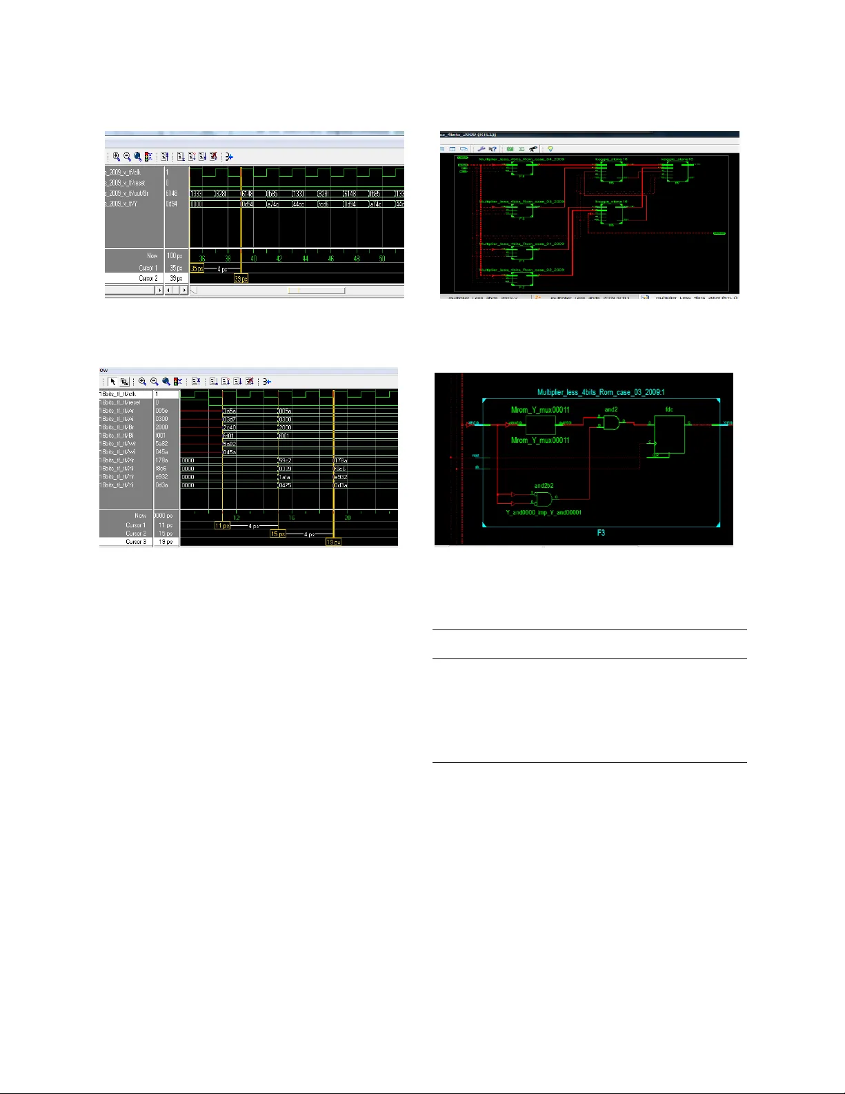
SN /HG Date: 9, 7. 2010 12: 00 Corresponding Author: Rozita Teymourzadeh, Institute of Microengineering and Nanoelectronics IMEN, VLSI Design Department, Universiti Kebangsaan Malaysia, 43600 Bangi, Selangor, Malaysia 1 On -Chip Implementation of Pipeline Digit-Slicing Multiplier-Less Butterfly for Fast Fourier Transform Architecture 1 Yazan Sam ir Algnabi, 1.2 Roz ita Teymourzadeh, 1 Masuri Othm an , 1 Md Shabiul Islam 2 Mok Vee Hong 1 Institute of MicroEngineering and Nanoe lectronics I MEN, VLSI D esign Departm ent, Un iversiti Kebangsaan Ma laysia, 43600 Bang i, Selangor, Malay sia 2 Faculty of Enginee ring, Architec ture and Built Envir onm ent, Electrical & El ectronic Engineering departm ent, UCSI University, Kuala Lum pur, Malaysia Abstract: The need for wireless co mmunication has driven t he co mmunication systems to high performance. However, th e main bottleneck that affects the co mmunication capability is the Fast Fourier Transform (FFT ), which is the core of m ost modulators. This study presents on-chip implementation o f pipeli ne d igit-slicing multiplier-less butterfl y for FFT struct ure. The ap proach taken; i n ord er to reduce computation complexity i n b utterfly, di git -slicing multiplier -less sin gle con stan t technique was utilized in the critical p ath o f Radix- 2 De ci mat io n I n T ime (DI T) FFT structure. The proposed design focused on t he trade -off between the s peed and active silicon area for the chip implementation. The new architect ure was investigated and simulated with MATL AB software. T he Verilog HDL c ode in Xilinx ISE environment was derived to de scribe the FFT B utterfly functionality and was do wnloaded to Virtex II FP GA board. Consequentl y, the Virtex -II FG4 56 Proto board w as used to imple ment and test the design on the rea l hard ware. As a res ult, fro m the findings, the synthe sis rep ort indicate s the maxi mum clock frequenc y of 549.75 MHz with t he total equivalent gate count o f 3 1,159 is a marked and significant improvement over Radix 2 FFT butterfly. In comparison with the co nventional butterfl y architect ure, design that can onl y run at a maximum clo ck frequency of 1 98.987 MHz and the conventional multiplier can only r un at a maximum clock frequency of 220.16 0 MHz , the propo sed system e xhibits b etter results . T he resulting maximum cloc k frequency increases by about 27 6.28% for the FFT butterfly and about 2 77.06% for the multiplier. It can be concluded that on-c hip i mplementation of pip eline digit -slicing multiplier-less butter fly for FFT structure is an enabler in solving prob lems that aff ect co mmunications capability in F FT and p ossesses huge potentials for future relat ed works and research ar eas. Key words: Pipelined digit-slici ng multiplier-les s; Fast Fourier T ransform (FFT); Verilog HDL; Xilin x INTRODUCTION FFT plays an i mportant role in many Digital Signals Processing (DSP) ap plications such as in communication systems a nd i mage pro cessing. I t is an efficient al gorithm to co mpute t he Discrete Fourier Transform (DFT). DFT is the main a nd important procedure in data a nalysis, system de sign, and implementation (Oppenheim a nd Rader, 1990 ). In ord er to red uce the complexity co mputation of the FFT algorithm many modules have been designed and implemented in d ifferent platfor ms. These mod ules focus o n the radix o rder o r twi ddle factors to perform a simple and efficient algorithm wh ich i ncludes t he higher radix FFT (Bergland, 19 69), the mixed -radix FFT (Singleton, 1969 ), the prime-factor FFT ( Kolba and Par ks, 1977) , the recursive FFT (Var konyi-Kocz y, 1995), low-memory reference FFT (Wang et al ., 2007) , Multiplier-less b ased FFT (Zhou et a l ., 2007; P rasanthi et al ., 200 5; Mahmud and Oth man, 2006 ) and Application-Spec ific Inte grated Circuit s (ASIC) syste m such as stated b y Baas ( 1999) . ASIC-based systems ar e able to fit real low-power o r high performance applications; however the function is ver y solid to be modified (Hs u and L in, 20 08). T he study of the d igit- slicing tech nique has b een d ealt by Bin Nun and Woodward ( 1976 ); P eled and L iu ( 1976 ) ; and Sharrif, (1980) for the digital filters. End time 2 Th e design and implementation of Digit -slicing FFT has been discussed by Sa mad et al ., (1998). T his stud y proposed a similar idea with the o nes put forth by Samad et a l ( 1998) ; but ha ving a di fference b y t he use of a different algorithm a nd different platfor m, which helps to improve the p erformance and ac hieve h igher speed. Recently, FPGAs Field Programmable Gate Array have become an ap plicable o ption to d irect hardware solution perfor mance in t he real time application. In this st udy, digit-slicing architect ure was proposed in design ing the pipeline digit-slicing multiplier-less butterfly. The FFT butterfly multiplication is the most crucial part in causi ng the delay in the co mputation o f the FFT . In vie w of the fact, the twiddle factors in the FFT processor were known in adva nce hence we prop osed to use th e pipeline digit sl icing multiplie r-less b utterfly to replace the traditional butterfly i n FFT. The study stru cture is organized as follows; describes the FFT architectur e in brief, e xplains t he butterfly co nventional archit ecture, disc uses the digit slicing architecture , explicates the desi gn of the pipeline digit- slic ing multiplier-less butterfly ar chitecture in detail and finall y the imple mentation re sult and conclusion respectivel y. Fast Fourier Transfor m (FFT): A usef ul method to transform do mains from th e ti me domain to the frequency domain and the reverse for the implementation on di gital hard ware is t he DFT. Fo r N - point DFT of a co mplex data sequence x (n) is defined in Eq. 1: N1 kn N n0 X(k ) x (n ) W , k 0, 1 , ..... .., N 1 (1) Where: x(n) and X(k) = Complex n umbers kn j2 / N N We = T he twiddle factor The DFT of N -point finite seque nce represents harmonically related frequenc y co mponents of x(n). The direct c omputation of Eq. 1 req uires the order of N 2 oper ati ons w he re N i s the tran sfo rm size. Cool ey and Tuk ey (1965) foun d thi s new techn iqu e to red uc e the orde r of complex ity operati ons o f DFT from N 2 to (Nl og 2 N). Con seq uent ly, a huge num ber of FFT alg orith ms have be en dev el oped su ch as Radix- 2, radix- 4 an d spli t radix algor ithm s. These algori thm s are mostly use d for practi ca l applic atio ns d ue to their simple st ructu re and con stan t bu tt erfly g eome try . In g ene ral, high er- radix F FT al go rit hm has f ewe r num bers of com plex mult ipli cat ions , w her eas radix- 2 FF T al gor ithm is the sim plest form in a ll FF T a lg orith ms. Fu rthe rmo re, it has a reg ulari ty mo de that m akes it sui ta ble f or VLS I im plem ent ati on as show n in th e fa llow ing Eq. 2: NN 11 22 nm m nm N N N n 0 n 0 22 X [m] x [ 2n ]W W x [ 2n 1 ]W (2) FFT algorithm relies on a ‘divide -and - conquer’ methodology, which divides the N coefficient points into smaller blocks in di fferent stages. The first sta ge computes with groups of t wo coefficients, yielding N/2 blocks, each computing the addition and subtraction of the co efficients scaled by the corres ponding twiddle factors, called a butterfly for its cross -over app earance as shown in Fig. 1. These results ar e used to co mpute the next state of N/4 blocks, wh ich will then combine the r esults of two previous blocks, co mbining four coefficients at this point. This process is repeated until o ne main blo ck is formed, with a final co mputation of all N coefficients. Fig . 2 shows the 8 -point radix -2 DIT FFT. Fig. 1: Butterfly structure . Fig. 2: 8-points FFT radix-2 Deci mation in Time. End time 3 Fig. 3: Rad ix -2 DIT FFT B utterfly Architecture . Conventional Butterfly architecture The conventional rad ix-2 DIT butterfly ar chitecture consists of co mplex d ata I/O, co mplex multiplier and complex adder and subtraction as shown in Fig. 3. Consider A a nd B as the co mplex input data, and the complex twiddle factor is co nsidered as W = Wr-jWi , hence fi nally the co mplex output are X and Y. Fig. 4: Complex multiplier structure Fig. 5: Complex Adder Structure The index r and i represent the real and imaginary pa rts respectively: X A W B (3) Y A W B (4) (X r jX i ) (A r j A i) (W r jW i) (B r jB i) ( 5) (Y r jY i ) (A r j A i) (W r j W i ) (Br j B i) (6) The implementation of the c omplex multiplier is required for four real multipli ers and t wo real ad ders a s shown in Fig. 4. T he complex multiplier is deter mined in Eq.7: (Br jBi) ( Wr jWi) (Br Wr ) ( Br jWi) ( jBi Wr ) ( jBi jWi ) [(Br Wr ) ( jBi jWi)] [(Br jWi) ( jBi Wr)] [(Br Wr ) (Bi Wi)] [(Br jWi) ( jBi Wr)] (7) The real and imaginar y p arts of the multiplicatio n result is )] ( ) [( Wi Bi Wr Br and )] ( ) [( Wr j B i jWi Br respectively. The complex adder is required for t wo re al adder s to perform addition functio nality as shown in Fig. 5. (A r jA i) (B r jB i) (A r B r) j (A i B i) (8) Digit-slicing arc hitecture: T he concept behind the digit-slicing architecture is a ny binary number that can be sliced into a few bloc ks o f s horter binary numbe r s, with eac h block carrying a different weight. In this study, the fi xed-point 2 ’ s comple ments arithmetic has been chosen to represent the input data, which are singed numbers with ab solute value les s than one. T he absolute val ue of the input data x with length of B bits (x 0 ,x 1 ,x 2 ,….,x B-1 ) has been represented in 2 ’ s complement as: B1 jj k0 x 2 x (9) To represent the sliced d ata, there ar e many different algorith ms. Depend ing on t he data type and word len gth, di fferent str uctures can be introduced . I n this stud y , where the fundamental sliced algor ithm will be presented as follo wing: b1 pk ( pb 1) k k0 x 2 X 2 (10) Where: x = Sliced into b b locks p = Bit widths per b lock p1 j k k , j j0 X 2 X (11) Where: X k,j =All either ones or zeros except End time 4 X k=b-1, j= p-1 = which is zero o r minus one The algorithm in Eq. (10) app lies when t he sliced data word length is 2 x such as 2 2 =4, 2 3 = 8, 16… bits. Thus, let us co nsider the decimal number -0.65625 o f which we would like to demonstrate how dig it slici ng operates acco rdingly: x = 1.010 1100 2 = -0.65625 10 where, the suffix 2 r efers to a binar y fixed point two ’ s complement number 8 bits and the suffix 10 r efers to a decimal number, if x is sliced into two blo cks, of each four bits wide, that is b = 2 and p = 4: 3 j 3 2 0 0, j j0 3 j 3 1 1 1, j j0 X 2 X 2 2 12 X 2 X 2 2 6 1 4 k ( 8 1) k k0 x 2 X 2 4 0 4 1 7 7 10 x 2 12 2 ( 6) 2 84 x ( 12 96) 2 0.65 625 128 Another a lgorithm that represent s the sliced data with a word length 2 x +1 such as 2 2 +1=5, 9, 17 … bits can be dealt as the follo wing: p1 k p k k0 x 2 X (12) Where, x is a d ecimal number whose ab solute value is less than o ne and is sliced into b blocks ea ch of p bits wide. The m ost sign ifi cant bl ock is k = 0 w here this con tai ns the only sig n bit of x plus leadin g dummy zeros to m ak e u p a block of len gth p bi ts (Sam ad et al ., 199 8): k0 p1 j k k , j k , j j0 X 0 or 1 onl y X 2 X ; X 0 or 1 only fo r k 0 (13) Let us assu me that t he decimal number - 0.328 125 is represented as ni ne bits two ’ s co mplement number: k 2 4 k k0 4 0 4 1 3 1 4 2 3 2 1 3 5 6 10 x 2 X x [2 ] [ 1 ] [ 2 ] [ 2 2 ] [2 ] [ 2 2 ] 1 2 2 2 2 - 0.328125 As a co mparison b etween the first and the second algorithms, the seco nd algorithm require s one extra block to deal with the sign bit which makes the design more co mplicated and requires more hard ware f or the implementation. In this study, the first digit -slicing algorithm has been chosen to build the digit -slicin g FFT butterfly structure. Therefore, any complex numbers, F, can be sliced i nto s maller b locks b, each having a shorter word length, p, as illustrated in following equations: RI F F j F (13) b 1 b 1 pk ( pb 1) pk ( pb 1) R k I k k 0 k 0 F 2 F 2 j 2 F 2 (14) Fig. 6: The digit-slici ng first algorithm for -0.65 625 Fig. 7: The digit-slici ng 2 nd algorithm for -0.32 8125 Fig. 8: Digit-slicin g structure for the input A. End time 5 p1 j R k R k , j j0 F 2 F (15) p1 j I k I k , j j0 F 2 F (16) Where , the values o f F Ik,i and F Rk,I are either zero or one. Pipeline digit-slicing multiplier-less butterfly architecture: The butterfly i s the s mallest component to b uild the FFT . As mentioned in the explanations prior to this, t he butterfly structure co ntains o ne complex multiplier, o ne c omplex adder, and one complex subtractor. The d igit-slicing arc hitecture has b een applied for the butterfly input to slice t he data in to four groups each carrying four bits as sho wn in Fig. 8 . Fig. 9: Digit-Slicing Single Constant M ultiplier (DSSCM) Struct ure. b1 pk ( pb 1) k k0 A 2 A 2 (17) p1 j k k , j j0 A 2 A (18) where, A k,j are all either o nes o r zeros except for A k=b-1,j=p-1 which is zero or minus one. The same applies for the input B : b1 pk ( pb 1) k k0 B 2 B 2 (19) p1 j k k , j j0 B 2 B (20) where, B k,j are all eit her one s or zeros except for the value B k=b-1,j=p-1 which is zero or minus one. The multiplicatio n functionalit y is regarded as the most impor tant op eration for most signal processing systems, but it is a co mplex and expensive operatio n. Many techniques have been introduced for reducing the size a nd i mproving the speed of multipl iers. So me applications r equire Constant Coef ficient Multiplier s such as digital signal processi ng, image p rocessing, and multiple p recision arithmetic in the design of compilers. Constant Co efficient Multipliers is one of the most common solutio ns to speed up the multiplication process. The multiplier ca n be designe d for one co nstant which is termed as Si ngle Constant Multiplier (S CM) or for many co nstant and i s termed as Mu ltiple Constant Multiplier (M CM). Since t he twiddle factor in FFT processor are known in ad vance, a special des ign of SCM has been proposed to perform the multiplication function with the twiddle factor w ithout usi ng t he traditional multiplier, which is ter med as Single Constant M ultiplier Less (SCML). T he design o f the SCML consists of four lookup tables ( ROMs) and adder to perform the output as shown in F ig 9. To generate the lookup tables data (the multiplication result possibilities), which are 16 different results for each ROM, a special MATLAB program has been written by applying the di git-slicing al gorithm for a ll the possib le numbers for the input data (4 b its) from “0000” to “1111” to per form all t he possibilities for t he multiplication resu lt. The result for the SCML has been optioned by simple addition for all the lookup tables ’ results. In the hardware implementation, the addition logic has been r educed. D uring t he addition o f t he four products obtained from the look -up tables, the least significant digit (4 b its) for eac h le vel is al ways added to zero. These b its will not b e affected, or change d a nd will be carried into the next colu mn. The storage o f all these possibilitie s in f our different ROMs allows the design to p erform the multiplication pro cess without any real multiplier. From Eq . 10 and 1 1, the digit -slicing multiplier is represented as the following: 3 4 k ( 7 ) k k0 BW 2 W B 2 (21) 3 j k k , j j0 WB 2 WB (22) where, WB k,j are all either o nes or zeros except for WB k=b-1,j=p-1 which is zer o or minus one and where W is the constant. End time 6 The result of the multiplication will be add ed and subtract ed with the co mplex inputs A r +jA i for the butterfly to perfor m the butterfly outputs. The butterfly output X has been d efined as: b1 pk ( pb 1) k k0 X 2 X 2 (23) p1 j k k , j j0 X 2 X (24) where, X k,j are all either o nes o r zeros except for X k=b-1,j=p-1 which is zero or minus one. By applying Eq. 17, 19 and 21 into Eq . 3: 33 4 k ( pb 1) 4k ( pb 1) kk k 0 k 0 3 4 k ( pb 1) k k0 k k k X A WB 2 X 2 2 A 2 2 WB 2 X A WB k k rk ik rk k r k ik k i k X is com plex numb er X X jX Re al part of X A WB Im ag part of X A WB The sa me step for the output X has b een app lied to get the output Y: b 1 b 1 pk ( pb 1) pk ( pb 1) kk k 0 k 0 b1 pk ( pb 1) k k0 k k k Y A WB 2 Y 2 2 A 2 2 WB 2 Y A WB (26) k k rk ik rk k r k ik k i k Y is com pl ex numb er Y Y jY Re al par t of Y A W B Im ag part of Y A W B Finally, the complex output is repr esented as the following: rk rk rk ik X A W B W B (27) ik ik ik rk X A W B W B (28) rk rk rk i k Y A W B W B (29) ik ik ik r k Y A W B W B (30) The full digit -slicing single co nstant multiplier-less has bee n desi gned a nd te sted in MATLAB as sho wn i n Fig 10 and 11 , of which the result is t hen co mpared with the normal mult iplier. For the additi on and sub tra ction , the paral le l-pref ix Kogg ie and Ston e Ling adde r wer e used for high spee d an d bette r perf orm ance . The pipe lin e techn iqu e was appl ie d f or th e f ull desig n for bet ter perf orm ance . RESULT Two different module s we re implemented for radix-2 DIT butterfly. The first module uses the conventional architecture for the butter fly where the twiddle factors are stor ed in ROM a nd called by the butterfly to be multiplied with the i nputs by utilising the dedicated high speed multiplier equipped with the Virtex-II FPGA. Fig. 10: MATLAB design o f Digit-Slicing Single Constant Multiplier -Less for the B utterfly. Fig. 11: MATLAB desi gn of Digit-slicing Butterfly. End time 7 Fig. 12: Simu lation result of the Pip eline Digit-slicing Single Constant M ultiplier-Less for t he Butterfly. Fig. 13: Simulation result of D igit-slicin g Butterfly. The other module uses t he pipelined d igit-slici ng single constant multiplier-less arch itecture to perform the multiplication with the twid dle factor. Both modules were built a nd tested in MATLAB as indicated in Fig. 9 and 10, and is then coded in Ver ilog and s ynthesized b y using the X ST-Xilinx Synthesis Tec hnology tool. The target FPGA was Xilinx Virtex-II XC2V500 -6-FG456 FPGA . The Model Sim sim ulati on res ult of pi pelin ed dig it- sli cing multi pli er- less radix- 2 DIT butte rfly is sh own in Fig. 12 an d 13, wh ile the synth esi s result s for th e two models are present ed in Tabl e 1, whi ch dem onst rat es the har dwar e spec ifi cati ons for the design. It indi cate s the maxim um clock frequ ency o f 549. 75 MHz for Pipe lin ed dig it-sl icin g Mul tip lier- les s But te rfly as well as th e Pipel ine d D igit- sli cing S ingl e Con st ant Multi plie r-l ess fo r the butterf ly with a perf orm anc e of the m aximu m clock fr equ ency of 609. 980 MHz . M eanw hi le, Fig . 14 and 15 sh ow s th e RTL sch emati c for the Pipel ine Digi t-Sl icin g Sin gle Con st ant Mu lti pli er-l ess for the But te rfly . Fig. 14: RTL schematic for the P ipeline Digit -slicing Single Constant Multiplier -Less for t he Butterfly. Fig. 15: RTL schematic for the P ipeline Digit -slicing Single Constant Multiplier -Less Lookup table (ROM) for the Butter fly. Table 1: Hardw are specifications of the digit-slicing butte rfly Xilinx Virtax- II Total equivalent ga te M aximum FPGA XC2v250-6FG456 count for desig n Frequency MHz Conventional bu tterfly 18.408 198.987 Pipeline Digit-Sl icing 3 1.159 549.750 Multiplier-le ss Butterfly Conventional 16 bits 4.131 220.160 Multiplier Pipeline Digit-Sl icing Single 6.483 609.980 Constant Multiplie r-Less 16 bits for the butter fly CONCLUSION This st udy presented an on -chip implementation of pip eline d igit -slicing multiplier-less butterfly for FFT structure. The implementation has been cod ed in Ver ilog hardware descriptive language and w as tested on Xilinx Vir tex-I1 XC2V500 -6- FG45 6 prototyping FP GA b oard. A maximum clo ck frequency of 549.75 MHz has been obtained from the synthesis re port f or th e p ipeline digit -slicing multiplier-less butterfly tha t is 2.77 tim e fa ster than the con ventional butterfly. It can be c oncluded that o n-chip End time 8 implementation of pipeli ne d igit -slicing multiplier-less butterfly for FFT struct ure is an enabler in solving problems that affect co mmunications cap ability i n FFT and p ossesses hug e potentials for future related w orks and research areas. REFERENCES Baas, B. M., 1999. A low-po wer, high-perfor mance, 1024 -point FFT processor. IE EE J. Solid-State Circuits , 34: 3 80-387. Bergland, G.D., 1969. A radix -eight fas t-Fourier transform subro utine for real -valued series. IEEE Trans. Audio E lectroacoust, 17: 1 38-144. Bin Nun, M.A. and M.E. Wo odward. 19 76. A modular approach to the hardware implementation of digital filters. Radio Elect. E ng . Cooley, J.W. and J. W. Tukey, 196 5. An a lgorithm for the mach ine calcula tion o f co mplex Fourier serie s. Math, Comp . , 19: 297-301. Hsu, Y.P. and S.Y. Lin, 200 8. Parallel-co mputing approach for FFT implementatio n on Digital Si gnal Processor ( DSP). W orld Acad. Sci. , Eng. Technol .,4 2 (2008) pp 587 -591. Kolba, D.P. and T.W. Parks, 1 977. A pri me factor FFT algorithm usin g hi gh -speed convolution. IEEE Trans Acoust. Speech, Signal Process, 25: 281-294. Mahmud, B . and M. Othman, 2006. FPGA implementation o f a ca nonical signed digit multiplier-less based FFT P rocessor for wireles s communication ap plications. I CSE2006 Proc ., Kuala Lumpur, Mala ysia, 2006. 641- 645 Oppenheim, A.V. a nd C.M. R ader, 1990. Discrete-Time Signal Processing . 2 nd Ed n., Up per Saddle River, Prentice-Hall, NJ, 0137549202. Peled, A. and B. Liu, 1 976. Digital Sig nal Processing Theory, Design and Implementation. Jo hn Wiley and Sons, US. Prasanthi, R., V. Anuradham, S.K. Sahoo and Cha ndra Shchar, 20 05. Multiplier less FFT Processor Architecture for Signal and Image P rocessing. ICISIP , 200 5 Vol. 2, No. 1, pp.35 – 45. Samad, S. A., A. Ra goub, M. Othman and Z.A.M. Sheriff, 1998. I mplem entatio n of a high speed fast Fourier transform V LSI c hip . Microelectronics J . UK., 29 (1998) pp881- 887. Sharrif Z.A.M., 19 80 . Digit slicing architectu re fo r real time digital filters. PhD thesis. Loughbor ough University.UK, 198 0. Sharrif, Z. A.M. and M. Othman, 198 9. A novel modular arc hitecture for VLSI Digital Si gnal Processing chip. CA -DSP ’ 89 , Oct. 11-14, lEE, Hong Kong. Singleton, R.C., 1969. An al gorithm for co mputing the mixed radix fast Fourier tra nsform. IEEE Trans. Audio Elect . , 17: 93- 103. Varkonyi-Kocz y, A.R., 199 5. A recurs ive Fast Fourier Transfor m algorit hm. IEEE Tran s. C ircuits Syst . 42: 614- 616. W ang, Y., Y. Tang, Y. Jiang, J.G. Chung and S.S. Song et a l ., 2007. Novel m emory refe rence reduction methods for FFT im plementation on DS P processors. IEEE Trans. Signal Process ., 55: 2338-2349. Zhou, Y., J .M. Nor as and S.J . Shephend, 2007. Novel design of multiplier-less FFT processors. Sig nal Proc. , 87 : 1402-1407.
Original Paper
Loading high-quality paper...
Comments & Academic Discussion
Loading comments...
Leave a Comment