A Programmable CMOS Transceiver for Structural Health Monitoring
We describe a highly-integrated CMOS transceiver for active structural health monitoring (SHM). The chip actuates piezoelectric transducers and also senses ultrasound waves received by the same or another transducer. The transmitter uses an integer-N…
Authors: Xinyao Tang, Haixiang Zhao, Soumyajit M
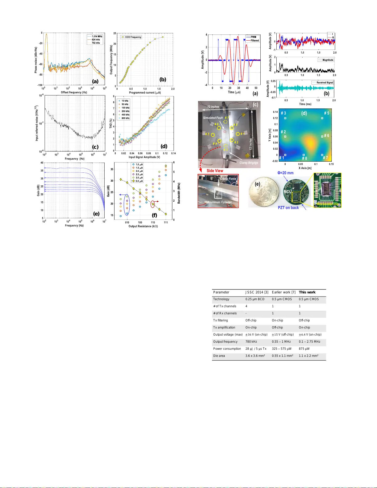
A Programmable CMOS T ranscei ver for Structural Health Monitoring Xinyao T ang, Haixiang Zhao, and Soumyajit Mandal Department of Electrical Engineering and Computer Science Case W estern Reserve Univ ersity , Clev eland, OH 44106 Email: sxm833@case.edu Abstract —W e describe a highly-integrated CMOS transceiver for active structural health monitoring (SHM). The chip actu- ates piezoelectric transducers and also senses ultrasound wav es recei ved by the same or another transducer . The transmitter uses an integer - N frequency synthesizer and pulse-width modulation (PWM) to generate low-distortion, band-limited wav eforms up to 12.7 V pp with center frequency from ∼ 0.1-2.75 MHz. The integrated offset-canceling fully-differential r eceiver has pr o- grammable gain and bandwidth, and uses quadrature demod- ulation to extract both amplitude and phase of the receiv ed wav eforms for further signal processing. The transcei ver was fabricated in a 0.5 µ m CMOS process and has been validated using (2D) damage localization on an SHM test bed. I . I N T RO D U C T I O N The health of the w orld’ s critical infrastructure, such as bridges, aircraft, and pipelines, is a subject of increasing concern. SHM enables real-time and continuous assessment of structural health by detecting the existence, location, and sev erity of potential damage. In activ e SHM, electrical pulses driv e an array of piezoelectric transducers attached to the struc- ture, which con v ert them to ultrasonic guided wa v es. These wa ves are recei v ed by another set of transducers and analyzed to determine structural health [1]. Lamb wav es have attractive propagation properties and are thus the most widely used ultrasonic guided wav es for activ e SHM. Howe ver , a v ariety of Lamb wav e modes with different velocities can propagate in the structure (see Fig. 1). The excitation wav eform is usually designed to only excite the lowest-order modes ( S 0 and A 0 ) in order to reduce the complexity of SHM signal processing. SHM systems are typically realized using discrete compo- nents. Howe ver , the size, weight, and power consumption of this approach makes it unattractiv e for emerging applications such as monitoring of aerospace structures [2]. This issue has been addressed using integrated piezoelectric drivers [3], [4] and flexible sheets that combine integrated circuits (ICs) and thin-film transistors for passiv e strain sensing [5], [6]. W e pro- pose a heterogeneous microsystem that integrates miniaturized electronics and sensors within a flexible substrate to further reduce system thickness, weight, and power , thus paving the way for scalable large-area SHM. W e have earlier i) designed and tested a current-controlled transceiv er IC in 0.5 µ m 2P/3M CMOS for this application [7], and ii) v erified its ability to detect structural damage [8]. Here we describe an improved digitally-controlled SHM transceiver and verify its ability to both detect and localize damage using a SHM test bed. Fig. 1: Dispersion of Lamb wa ves in a 1.5-mm-thick Alu- minum plate: (a) variation in group velocity with frequency; (b) illustration of plate deformation in the A 0 and S 0 modes. I I . C H I P D E S I G N A block diagram of the proposed IC is shown in Fig. 2. The transceiv er runs off 5 V and is digitally-controlled through a standard serial peripheral interface (SPI) port. An integer- N frequency synthesizer generates programmable output frequen- cies (0.8–22 MHz) from a reference clock, thus allo wing a single stable reference to be distrib uted to the entire SHM network. The synthesizer output is fed into a 4-bit PWM modulator that generates predefined pulse widths based on data stored in on-chip memory (R OM). The widths are chosen to minimize the least-square error between the reference (a 5- cycle Hamming-windo wed sinusoid) and the dif ferential PWM outputs after a low-pass filter (LPF). The latter can driv e signals up to 10(4 /π ) = 12 . 7 V pp into the transducer . Q u a d r a tu r e M i x e r L N A I + I - Q + Q - S P I C o n t r o l & M e m o r y ÷ 4 ÷ 2 I n t e g e r - N s y n t h e s i ze r P W M L P F & P G A L P F & P G A L P F & P G A L P F & P G A B u ffe r 0 B u ffe r 1 B u ffe r 2 B u ffe r 3 B u ffe r 4 18 0 o 0 o En C l k M O S I 32 . 7 6 8 k H z Fu l l y - di f f e re n t i a l R e c e i v e r T ra n s m i t t e r B i t [ 21 : 57 ] B i t [ 0 : 20 ] O f f C h i p V d d = 5 V P Z T 0 o & 90 o 1 8 0 o & 2 7 0 o S P I I n p u t s R e f e r e n c e C l o c k D i f f . ADC # 1 D i f f . ADC # 2 D u p l e x e r Φ 1 : T r a n s m i s s i o n Φ 2 : R e c e p t i o n L P F Φ 1 Φ 2 Fig. 2: Block diagram of the proposed SHM transceiv er IC. The fully-differential recei ver uses a low-noise amplifier (LN A) with programmable gain and bandwidth. The LNA out- puts are down-con verted to baseband using a passiv e double- balanced quadrature mixer . T wo stages of low-pass filters and programmable-gain amplifiers are implemented for further filtering and amplification. The four complex outputs ( I + , I − , Q + , Q − ) retain both the amplitude and phase of the input signal, and are digitized by an off-chip ADC for further processing. The whole recei ver is biased through a constant G m current reference and programmed over SPI. It can also be put into a low-po wer shutdown mode between pulses. A. Low-Distortion Pr ogr ammable T ransmitter Modern activ e SHM algorithms, such as delay-and-sum and matched filtering, are implemented through baseline subtrac- tion. Therefore, low-distortion and highly-accurate excitation wa veforms are desired to reduce the false alarm rate (F AR) during long term SHM. Our solution uses (i) an integer- N synthesizer based on a fourth-order loop filter that uses a low-phase-noise 32 . 768 kHz reference clock; and (ii) a PWM scheme with predefined transitions based on a priori knowledge of the desired SHM excitation signal after off-chip LC low-pass filtering. This design allows the center frequency of the outputs to be programmed from 0.1-2.75 MHz, thus allowing a wide variety of structures to be studied. Fig. 3 shows the design of the main transmitter blocks in more detail. The synthesizer, sho wn in Fig. 3(a), includes a wide-linear-range transconductor (WLR), 5-bit NMOS and PMOS current D A Cs, and a current-starved ring oscillator (CCO). This allows the loop bandwidth to be controlled through the N- and P-DA Cs; in particular , we can make the bandwidth and phase margin independent of the division ratio ( N ). The synthesizer also uses a sequential phase frequency detector (PFD), a cascoded charge pump, and a passive third- order loop filter . The charge pump uses dif ferential switching to reduce charge injection errors. The loop filter contains two high-frequency poles that are placed beyond the crossover frequency of the loop. These poles filter out high-frequency ripples on the control voltage ( V LOO P ), thereby reducing jitter in the output clock while only minimally de grading phase margin. The WLR conv erts V LOO P to a current; it combines a well-input differential pair with other linearization techniques to achiev e > 1 . 5 V input linear range. The loop bandwidth is set to 3.5 kHz (about 10% of the nominal reference frequency) to av oid degradation of phase margin due to the phase lag inherent in a discrete-time PFD; the desired value is set to 50 ◦ . Fig. 3(b) sho ws the block diagram of the 4-bit PWM. T o generate fully-differential excitation pulses, it uses two XOR gates and a 180 ◦ delay circuit. The final pulse widths, as shown in Fig. 3(b), for the up-side and down-side are set as multiples of the synthesizer output period ( 1 , 5 , 7 , 3 and 3 , 7 , 5 , 1 , respectiv ely). The PWM outputs are filtered using an of f-chip LC LPF in which the C is pro vided by the transducer itself. B. Of fset-Canceling Fully-Differ ential Receiver The implementation of the SHM receiver is shown in Fig. 4. A trigger pulse Φ t initiates the measurement. RST and OPER 4 -b i t C o u n t e r D 1 D i g i t s T i m e 4-b i t R e g i s t e r 4-b i t R e g i s t e r ( L S B ) ( M S B ) B 0 B 3 ( L S B ) ( M S B ) A 0 A 3 4 -b i t C o m p a r - a t o r Pulse Modulation B i t [ 0 : 3 ] 1 1 1 0 1 0 1 0 0 0 1 0 0 1 1 0 4 x 4 - b i t R O M S h i f t R e g i s t e r C o n t r o l L o g i c U p Pu l s e D o w n Pu l s e XO R XO R PA #2 PA # 1 T i m e A m p l i tu d e P W M F i l t e r e d C l k P Z T (b ) C l k ÷ 4 P F D V d d UP DN R 1 R 2 C 1 C 2 C 3 Loop Filter W LR O T A Gm V REF ÷ N B i t [ 0 : 4 ] B i t [ 0 : 4 ] B i t [ 0 : 9 ] N - DAC P - DAC CCO P rog ra m m a b l e N D i v i d e r C l k R e f . To P W M (a ) I B I A S V LOOP Fig. 3: Low-distortion programmable transmitter circuit de- sign: (a) block diagram of the integer- N synthesizer; (b) digitally-defined PWM transition times. are two non-overlapping clock signals deri ved from Φ t . During the RST phase, each block resets to the input common- mode v oltage V C M = 1 . 3 V . Auto-zeroing is used within each LPF and programmable-gain amplifier (PGA) for offset cancellation. The receiv er operates during the OPER phase. A fully-differential cascoded low-noise amplifier (LNA), as shown in Fig. 4 (a), is used as the first signal processing stage. The circuit uses a simple resistiv ely-loaded differential pair and has an input-referred thermal noise PSD of v 2 n,in ≈ 8 k T γ /g m , where γ ≈ 2 / 3 and g m is the transconductance of each transistor in the input pair . A replica bias circuit generates a reference voltage V ref that is nominally equal to the DC output voltage of the LNA. This voltage is used to set the common-mode input lev el of a differential buf fer . W e also use 3-bit resistor and bias current D ACs for programmable LN A gain and bandwidth. T ypically , at a bias current of 3 µ A and a 40 k Ω load, the LN A has a simulated small-signal gain of 21.6 dB, a bandwidth of 4.3 MHz, a 1 /f corner frequency of 10 kHz, and an input-referred thermal noise PSD of 21 nV/Hz 1 / 2 . The input linear range, defined using total harmonic distortion (THD) < 5 %, is ∼ 60 mV and ∼ 70 mV for input frequencies of 400 kHz and 1.2 MHz, respectively . The differential buf fer isolates LN A outputs from the pas- siv e double-balanced quadrature downcon version mixer (see Fig. 4(b) and (d)). The buf fer uses two common-mode feed- back (CMFB) amplifiers, one for each gain stage. A passiv e mixer design was chosen because of its small area, absence of static power consumption, and high linearity , while the double-balanced topology ensures high isolation between the ports. The typical con version loss is − 4 dB. Quadrature local oscillator (LO) signals for the mixers are generated from the same synthesizer used in the transmitter , resulting in a direct con version (zero-IF) architecture. An external LO input also allows the receiv er to be characterized at non-zero IF . V CM M 1 M 2 V cl k V c l k 0 0 C ov C ov / 2 R S T R S T O P E R V CM C 1 C 2 A 1 V R E F A 2 C 3 C 4 C 5 C 6 V RE F O P E R V R E F R S T R S T R S T R S T V CM Gm 1 Gm 2 4-bi t C a p D A C 0 . 1 ~ 1 . 7 pF V CM V R E F A 3 C 9 C 10 C 11 C 12 V R E F O P E R V CM R S T R S T R S T R S T 0 o 90 o C l k R EF V CM V CM O P E R RS T R S T R S T R S T C 7 C 8 C 13 C 14 O P E R LN A M i xe r LP F + P G A Bu ffe r Bu ffe r I+ , I- Br an c h Q+ , Q- Br an c h S t age 1 S t age 1 I B I A S 1 v i n + v i n - V d d V R E F v o u t - v o u t + 3 -bi t DAC 3 -bi t DAC 3 - bi t DAC A 1 Gm V d d V d d v out - v out + v i n - v i n + v out + v ou t - V CM V CN V CN V CP V CP V CN V CN I B IA S 3 I B IA S 3 V d d V d d v i n - v i n + vo + vo - vo + vo - V CM 1 V CM 1 V CM 2 v ou t + v out - v out + v out - I B IA S 2 I B IA S 2 R 1 R 2 C f C f C M F B S t age 1 C M F B S t age 2 C M F B A 2 &A3 (a) (b ) (c) (d) (e ) F r om P ZT To S tage 2 L P F & PGA B u f f e r Fig. 4: Block diagram of the fully-differential receiv er and its circuit design: (a) LNA with low-leakage-current switches; (b) LPF and PGA blocks in stage # 1 after the passi ve mixers; (c) LN A circuit with programmable 3-bit resistor D AC; (d) fully-differential buffer with two stage CMFB; (e) fully-dif ferential WLR O T A. A second-order G m - C LPF remov es the upper mixer side- bands. It uses a fully-differential WLR OT A with continuous- time CMFB, as shown in Fig. 4(e). The LPF cut-off frequency can be programmed using a 5-bit current DA C and a 4- bit capacitor D A C (up to 1.5 pF). The PGA circuit reuses the same OT As as in the LPF , with one acting as a V - I con verter and the other as a buf fered resistor . The voltage gain G = G m 1 /G m 2 ≈ I B ias 1 /I B ias 2 is set by two 5-bit current D ACs, where the approximation is v alid in subthreshold.c Fig. 5: Die photograph of the proposed transceiver IC. I I I . E X P E R I M E N T A L R E S U L T S A proof-of-concept SHM transceiv er IC was fabricated in the OnSemi 0.5 µ m CMOS process. Fig. 5 shows a die micro- graph of the proposed IC, which has a acti ve area of 1.1 mm × 2.2 mm. The chip is po wered from a single 5.0 V supply with av erage po wer consumption of 875 µ W . Fig. 6(a) shows measured phase noise, which decreases to about -70 dBc/Hz at an offset of 10 Hz, while the transmitter tuning curve is shown in Fig. 6(b). Figs. 6(c) and (d) show the measured input-referred noise PSD and THD, respectiv ely , of the LN A and buf fer . The thermal noise floor and maximum input signal amplitude (defined by THD < 5 ) are in good agreement with simulations. Given that the receiv ed signal amplitude in activ e SHM is typically ∼ 0.5 mV to 20 mV (depending on the sensor location), the proposed LNA provides sufficient linear range. Fig. 7 shows the IC connected to an SHM test bed (1 foot 2 area). The bare dies were wire-bonded to miniature (diame- ter = 20 mm) wired sensor nodes fabricated (see Fig. 7(e)). Each sensor node also contains a microcontroller (MCU; Atemel SAM L21E) for programming, digitization, signal processing and communicating with the system controller . The PZT transducer ( 6 × 6 × 0 . 5 mm) is connected to the back of the PCB. Fig. 7(b) sho ws typical receiv er outputs ( I and Q ). The reconstructed signal amplitude follows the en velope of the input signals, as expected. Fig. 7(d) shows an example of successful 2D localization of structural damage using the custom IC and an array of 8 PZT transducers mounted on a 3 mm-thick aluminum plate. Rev ersible damage is introduced as an stressed point loaded by clamps (see Fig. 7(c)). The damage map was generated by using the delay- and-sum localization algorithm on data recorded from the IC. Fig. 8 compares the performance of our chip with recently- reported driver ICs for acti ve SHM applications [3], [7]. I V . C O N C L U S I O N W e hav e i) presented a digitally-programmable single-chip transceiv er for active SHM using ultrasonic guided wav es, and ii) successfully localized damage on a SHM test bed using the proposed chip and a delay-and-sum algorithm. Future work will focus on i) further miniaturization of the sensor nodes by integrating an analog-to-digital con verter (ADC) and custom digital signal processor (DSP) on the chip; and ii) eliminating the wired bus by using ultrasonic power and data transfer . ( e ) ( f ) ( d ) ( c ) ( a ) ( b ) Fig. 6: Chip measurement results: (a) phase noise for synthe- sizer output frequencies of 624 kHz, 702 kHz and 1.014 MHz; (b) CCO output frequency range; (c) input-referred noise of the LNA and buf fer; (d) THD of the LN A and buf fer; (e) measured gain of the LN A at 3.0 µ A; (f) measured LN A gain and bandwidth in different scenarios. R E F E R E N C E S [1] A. Raghavan and C. E. S. Cesnik, “Review of Guided-wav e Structural Health Monitoring, ” The Shock and V ibration Digest , vol. 39, no. 2, pp. 91–114, Mar 2007. [2] W . Staszewski, S. Mahzan, and R. Traynor , “Health monitoring of aerospace composite structures Activ e and passive approach, ” Compos- ites Science and T ech. , vol. 69, no. 11-12, pp. 1678–1685, Sep 2009. [3] Y . Guo, C. Aquino, D. Zhang, and B. Murmann, “A Four-Channel, +/-36 V , 780 kHz Piezo Driver Chip for Structural Health Monitoring, ” IEEE Journal of Solid-State Circuits , vol. 49, no. 7, pp. 1506–1513, Jul 2014. [4] R. Pierco, G. T orfs, J. V erbrugghe, B. Bakeroot, and J. Bauwelinck, “A 16 Channel High-V oltage Driver with 14 Bit Resolution for Driving Piezoelectric Actuators, ” IEEE Tr ansactions on Circuits and Systems I: Re gular P apers , vol. 62, no. 7, pp. 1726–1736, Jul 2015. [5] Y . Hu, W . S. A. Rieutort-Louis, J. Sanz-Robinson, L. Huang, B. Glisic, J. C. Sturm, S. W agner, and N. V erma, “Large-scale sensing system combining lar ge-area electronics and CMOS ICs for structural-health monitoring, ” J. Solid-State Circ. , vol. 49, no. 2, pp. 513–523, Feb 2014. [6] Y . Hu, L. Huang, W . S. a. Rieutort-Louis, J. Sanz-Robinson, J. C. Sturm, S. W agner, and N. V erma, “A self-powered system for large-scale strain sensing by combining CMOS ICs with large-area electronics, ” IEEE Journal of Solid-State Circuits , vol. 49, no. 4, pp. 838–850, Apr 2014. [7] H. Zamani, C. Chen, X. T ang, P . Mohseni, and S. Mandal, “ A current- controlled transceiv er ic for structural health monitoring, ” in IEEE New Cir cuits and Systems Conference (NEWCAS) , June 2016, pp. 1–4. # 1 # 2 # 3 # 5 # 6 # 7 # 8 # 4 S i m ul a t e d Fa ul t C l a m p B r i gdg e Side Vie w A l um i num C y l i nde r C l a m p Fo r c e 1 2 i nc he s 1 2 i nc he s (c ) Φ = 20 mm M C U P ZT on ba c k W i r e - bon de d c hi p ( e) (d) (d ) # 1 # 2 # 3 # 5 # 6 # 7 # 8 ( b) (a) Fig. 7: Experimental ev aluation in a SHM test bed: (a) measured PWM digital output of the transmitter, and smooth Hamming-like wav eform generated across the piezoelectric transducer after low-pass filtering; (b) typical I and Q outputs from the SHM receiv er, reconstructed signal magnitude, and the raw signal; (c) experimental setup in an SHM test bed;(d) 2D damage localization results from the sensor node using delay-and-sum algorithm; (e) miniaturized SHM sensor node containing a commercial MCU and the SHM IC. Pa ra m e t e r J SSC 2 0 1 4 [ 3 ] Ea rl i e r w o rk [ 7 ] T h i s w o r k T e ch n o l o g y 0 . 2 5 μ m BC D 0 . 5 μ m C MO S 0 . 5 μ m C MO S # o f Tx ch a n n e l s 4 1 1 # o f R x ch a n n e l s - 1 1 Tx f i l t e ri n g O f f - ch i p On - ch i p O f f - ch i p Tx a mp l i f i ca t i o n On - ch i p O f f - ch i p On - ch i p O u t p u t vo l t a g e (ma x ) (o n - ch i p ) (o f f - ch i p ) (o n - ch i p ) O u t p u t f re q u e n cy 7 8 0 kH z 0 . 5 5 – 1 MH z 0 . 1 – 2 . 7 5 MH z Po w e r co n su mp t i o n 2 8 µ J / 5 µ s Tx 325 – 5 7 5 µ W 8 7 5 µ W D i e a re a 3 . 6 x 3 . 6 mm 2 0 . 5 5 x 1 . 1 mm 2 1 . 1 x 2 . 2 mm 2 Fig. 8: Comparison of the proposed chip with recently-reported driv er ICs for SHM applications. [8] X. T ang, H. Zhao, and S. Mandal, “ A highly-integrated cmos transceiv er for acti ve structural health monitoring, ” in National Aerospace and Electr onics Confer ence (NAECON) , July 2016, pp. 133–138.
Original Paper
Loading high-quality paper...
Comments & Academic Discussion
Loading comments...
Leave a Comment