Direct Conversion Pulsed UWB Transceiver Architecture
Ultra-wideband (UWB) communication is an emerging wireless technology that promises high data rates over short distances and precise locationing. The large available bandwidth and the constraint of a maximum power spectral density drives a unique set…
Authors: Raul Blazquez, Fred Lee, David Wentzloff
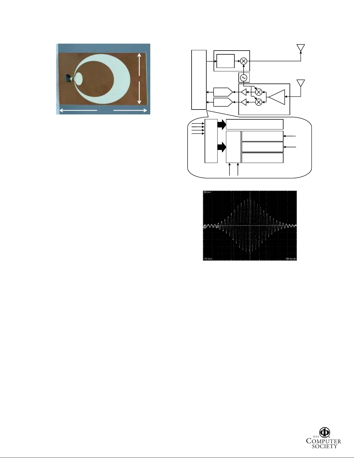
Direct Conversion Pulsed UWB Transceiver Architecture Raúl Blázquez, Fred Lee, David Wentzloff, Brian Ginsburg, Johnna Powell, Anantha Chandrakasan Massachusetts Institute of Technology 38-107, 50 Vassar St., Cambridge, MA 02139, USA rbf@mit.edu Abstract Ultra-wideband (UWB) communication is an emerging wireless technology that promises high data rates over short distances and precise locationing. T he large available bandwidth and th e constraint of a maximum power spectral density drives a unique set of system challenges. This paper addre sses these challenges using two UWB transceivers and a discrete prot otype platform. 1. System considerations The use of ultra-wideband si gnals for communication purposes is approved by the FCC from 3.1 to 10.6 GHz with a maximum effective isotropic radiated power spectral density of -41.3 dBm /MHz. An effective high data rate transceiver in this ba nd should provide robust communication under severe multip ath conditions (rms delay spread of the channel o n the order of 20 ns) and narrowband interferers. In addition, a fast signal acquisition algorithm must be im plemented to reduce t he duration of the preamble to a value comparable with current wireless systems (~20 µs). The RF Front-end must m eet the specifications on noise figure and linearity ov er a bandwidth larger than 500 MHz. The im pulse responses of both the antenna and the RF front-end add to that of the channel. Since the receiver will only be able to deal with a maxim um channel impulse response set by design, the RF front-end must be designed to meet this constraint. The ADC requires sampling rates larger than 500 MSps. The specification of the data converter resolution determines not only its power dissi pation but also that of the digital back end. A 1-bi t analog-to-digital converter (ADC) in a noise limited regim e, and a 4-bit ADC in a narrowband interferer re gime are sufficient [1]. The back end requires parallelization to reduce the packet synchronization time and to process the large data rate provided by the ADC. The inter-symbol interference (ISI) due to multipath can be addressed with a Viterbi demodulator. The energy spread ca used by the multipath can be compensated using a RAKE re ceiver. These elements require an estimation of the impulse res ponse that may be obtained during the pac ket synchronization. The frequency of an interferer m ay also be estimated in the digital back end. The large complexity required in the synchronization an d demodulation of the UWB signal results in more than half of the system power being dissipated in the digital back end and t he ADC. 2. First generation transceiver Fig. 1 shows a system -on-a-chip transc eiver for baseband puls ed UWB signals [2] that was implem ented using a 0.18 µm CMOS technol ogy at 1.8 V in a 4.3 mm × 2.9 mm die. A wireless link of 193 kbps was demonstrated with this transceiver. The RF front does not require a down converte r. The analog-to-digital converter is a 4-way time-interleaved flash ADC that performs an initial 4-way parallelization of the signal. The timing synchronization is fully performed in the digital back end. Through further parallelization, packet synchronization is obtained in less tha n 70 µs. Correl ato r 2 G SPS FLAS H I n terleave d An a l o g to Digital Con verte r RF Front E n d High Speed Buffe rs PL L Fine Tracking Coarse Acquisition T r ansm i t ter Correlato r High Speed Buffe rs FLASH ADC Coarse Acquisition Subsystem Correlators Correlators Parallellizer Parallellizer PLL Fine Tracking Subsystem RF Front-end Figure 1. Single chip UWB transceiver. Proceedings of the Design, Automation and Test in Europe C onference and Exhibition (DATE’05) 1530-1591/05 $ 20.00 IEEE 3. Architecture of a 3.1-10.6 GHz transceiver We are currently developing a sec ond generation UWB system to operate in the 3.1-10.6 GHz band. The signal is comprised of a sequence of 500 MHz bandwidth pulses that are upconve rted to one of 14 channels (sub- bands) in the 3.1-10 .6 GHz band. The system is design ed to transmit 100 Mbps. An electrically sm all planar antenna [3] of only 4.2 cm × 2.7 cm has been devel oped (Fig. 2). The block diagram of the receiver is shown i n Fig. 3. The RF front end uses a direct conversion architecture. Both in-phase and quadrature channels are then digitized using two 5-bi t successive approximation register ADCs that feed the digital ba ck end. In order to cope with the multipath, the channel impulse response is estimated with a precision of up to four bits during the packet pream ble. This information is used in a RAKE receiver a nd in a Viterbi demodulator, both of them program mable. The digital back end detects the presence of an interfe rer and estimates its frequency that may be used in the front end notch filter. Th is receiver allows us to trade off power dissipation with signal processing com plexity, quality of service and data rate, adapting to channel co nditions. A discrete prototype with the same specifications has been designed and implemented , allowing not only the testing of the different parts of the transceiver for specifications, but also a complete testing of the algorithms implemented in the digital back end under realistic conditions. This plat form is also flexible enough to generate all kinds of signals within a bandwidth of 500 MHz, allowing the comparis on between different modulation schem es. Fig. 4 shows an example of a modulated pulse used in this discrete prototype. 4. Conclusions The key system challenges for UWB communication systems are outlined in th is paper. The design trade-offs are illustrated using two di fferent UWB transceivers and a discrete platform. Acknowledgements This research is sponsored by Hewlett-Pack ard under the HP/MIT Alliance and th e NSF under contract ANI- 0335256. References [1] R. Blazquez, F. Lee, D . W e n t z l o f f , P . Newaskar, J. Powell, A. Chandrakasan, “Digital archit ecture for an ultra- wideband radio receiver”, in Proc. Vehicu lar Technology Conf., 2003-Fall, Vol. 2, pp. 1303-1307 . [2] R. Blazquez, P. Newaskar, F. Lee, A. Chandrakasan, “A baseband processor for pulsed ultra-wideband signals,” in Proc IEEE Custom Integrated Circuits Conf., 2004, pp. 587-590. [3] J. Powell, and A. Chandrakasa n, “Differential and single ended elliptical antennas for 3.1-10.6 GHz ultra wideband communication,” in Proc. IEEE Antennas and Propagation Society International Symposium , 2004, Vol. 3, pp. 2935- 2938. 42 mm 27 mm Fi g ure 2. Planar antenna for UWB. Figure 3. UWB system block diagram. Figure 4. 500 MHz pulse with carrier 5 GHz. 580 ps/div 150 mV -150 mV Pulses per bit S p ectral Monitorin g Correlators Channel Est. Viterbi Demo d PLL/DLL PRF Precision States Retiming Block Samples Di g ital Back en d Transmitte r Pulse Frequency Synthesizer ADC LNA RF Front-end ADC Proceedings of the Design, Automation and Test in Europe C onference and Exhibition (DATE’05) 1530-1591/05 $ 20.00 IEEE
Original Paper
Loading high-quality paper...
Comments & Academic Discussion
Loading comments...
Leave a Comment