An Improved FPGA Implementation of the Modified Hybrid Hiding Encryption Algorithm (MHHEA) for Data Communication Security
The hybrid hiding encryption algorithm, as its name implies, embraces concepts from both steganography and cryptography. In this exertion, an improved micro-architecture Field Programmable Gate Array (FPGA) implementation of this algorithm is present…
Authors: ** - 원저자: 논문에 명시되지 않음 (일반적으로 “SAEB” 그룹) - 소속: DATE 2005 논문집 (Design, Automation, Test in Europe) **
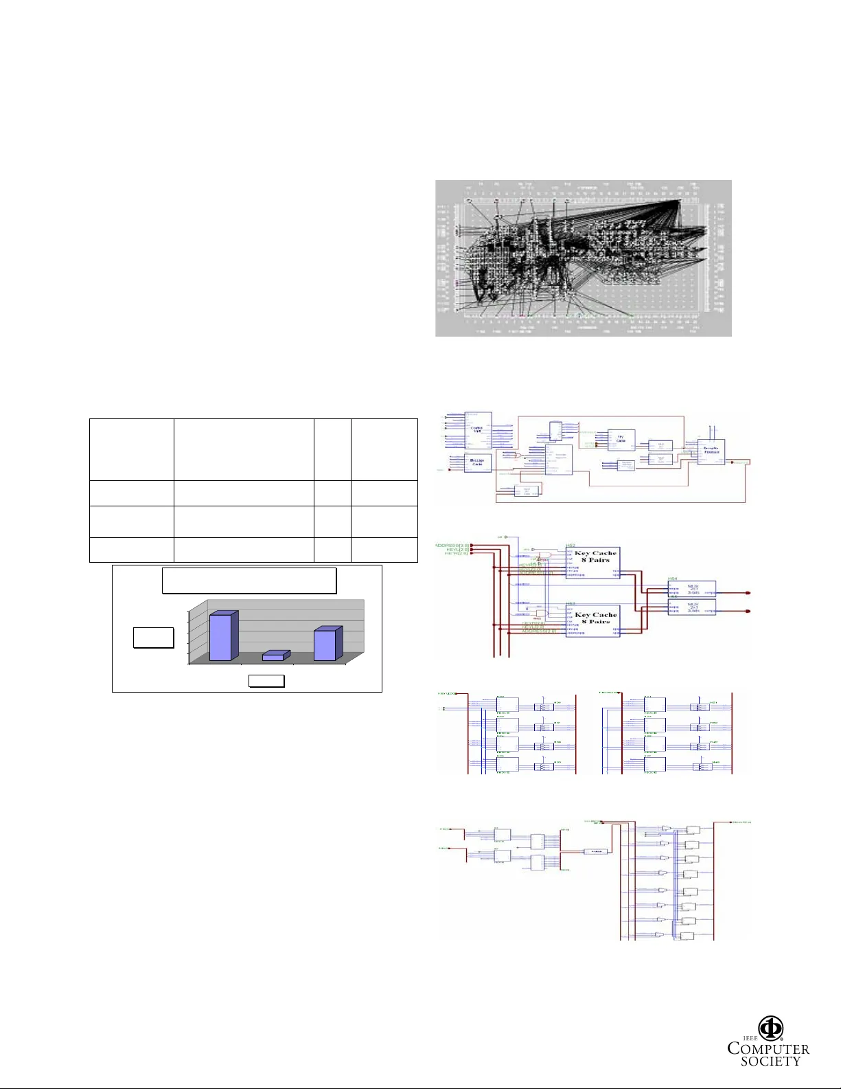
A N I MPRO VED FPGA I MPLEMENT A TION OF THE M ODIFIED H YBRID H IDING E NCR YPT ION A LGORITHM (MHHEA) FOR D ATA C OMMUNICA TION S ECURITY Hala A. Farouk, Magdy Saeb Arab Academy for Science, Technolog y & Maritime Transport School of E ngineering, Computer Department Alexan dria, Egypt E-mail : mail@magdysaeb.ne t Abstract The hybrid hiding encryption algorithm, as its name implies, embraces concepts from both steganography and cryptography. In this exertion, an improved micro- architecture Field Programmable Gate Array (FPGA) implementation of this algorithm is presented. This design overcomes the observed limitations of a previously- designed micro-architecture. These observed limitations are: no exploitation of the possibility of parallel bit replacement, and the fact that the input plaintext was encrypted serially, which caused a dependency between the throughput and the nature of th e used secret key. This dependency can be viewed by some as vulnerability in the security of the implemented micro-architecture. The proposed modified micro-architecture is constructed using five basic modules. These modules are; the message cache, the message alignment module, the key cache, the comparator, and at last the encryption module. In this work, we provide comprehensive simulation and implementation results. Th ese are: the timing diagrams, the post-implementation timing and routing reports, and finally the floor plan. Moreover, a detailed comparison with o ther FPGA imp lementati ons is m ade ava ilable and discussed. Keywords: FPGA, micro-architecture, data communication security, encryption, steganography, cryptography, algorithm. I. I NTRODUCTION In this work, we present an FPGA-based micro- architecture implementation of a modified version of the encryption algorithm entitled “Hybrid Hiding Encryption Algorithm (HHEA)” [SHAAR03] . In the basic version of this algorithm, no conventional substitution and translation operations on the plaintext characters are used. It rather uses simple plaintext hiding in a random bit s tring called the hiding vector. The name “Hybrid” is used to show that this encryption algorithm has built-in features that are inherited from data hiding techniques or "Steganography". As a matter of fact, one can use the m icro-architecture for both steganography and cryptography depending o n the user approach and the proper selection of the key. The basic version of this algorithm was previously implemented, as shown in reference [SAEB04a] . However, this approach did not exploit the possibility of parallel bit replacement. Furthermore, the input pl aintext was encrypted serially, which caused some dependency between the throughput and the nature of the key. This dependency can be viewed by some as vulnerability in the security of the implemented micro-architecture. Based on these observations and to eliminate certain types of cipher attacks, we decided to present a modified algorithm and its accompanying micro-architecture that overcomes such limi tatio ns. The modi fied desi gn elim inates th e dependency between the micro-architecture throughput and the key. It also provides a significant performance improve men t by ful ly explo iting the in heri ted pa rall eli sm originated by the algorithm . Moreover, the modified version escapes the chosen-plaintext attacks. In the next few sections we discuss the modified algorithm, the building blocks of the proposed improved micro- architecture along with de tails of its operation, the simulation and implementation results. The details of the carried out simulations, timing, rou ting reports and the floor plan are completely provided in the given appendix. Moreover, we present a comparison with other implementations of a selected group of encryption algorithms [SAEB02] , [SAEB02] . II. T HE A LGORITHM In the following few lines, we provide a su mmary of the MHHEA algorithm [SHAAR03] . The aim of the algorithm is hiding a number of bits from plain text message (M) Proceedings of the Design, Automation and Test in Europe C onference and Exhibition (DATE’05) 1530-1591/05 $ 20.00 IEEE into an N-bit long random vector (V). The locations of the hidden bits are determined by the key (K). Algorithm MMHHEA [Given a plain text message M , key matrix K Lx2 , scrambled key matrix KN Lx2 where i =0,…., L; L 15 k ij ^` 7 , 6 , 5 , 4 , 3 , 2 , 1 , 0 j =1,2 The aim of the algorithm is hiding a num ber of bits from plain text message (M) into a random vector (V) of bits. The locations of the hidde n bit s ar e deter mined by t he key K Lx2 ] Input: M, K Lx2 , Output: en crypted file Algorithm Body: i: =0, m:=0 M[0]: =first digit in M file while (M[m] EO F) [EOF: End Of F ile] i: = i mod L Generate 16-bit randomly and set them in V Vector if (K i,1 K i,2 ) then z: =K i,1 K i,1 : =K i,2 K i,2 : =z // Scramble the h iding location us ing the high order bits of the hiding vector KN i,1 :=V[K i,2 +8 down to K i,1 +8] XOR K i,1 KN i,2 := KN i,1 +(K i,2 - K i,1 ) mod 8 if (KN i,1 KN i,2 ) then z: =KN i,1 KN i,1 : =KN i,2 KN i,2 : =z // Scramble the message bits using the o riginal key q:=0 for j= KN i,1 to KN i,2 q:=q mod 3 if (M[ m] EOF) then do V [j]=M[ m] XOR K i,1 [q] m: = m+1; next m in M file q:=q+1 end do next j Save V in output file i: =i+1 end while; End algorithm. In this algorithm , we have scrambled the location an d the message to overcome constant chosen-plaintext att ack. III. T HE M ICRO - ARCHITECTURE In this section we describe the micro-architecture with its operation details using a finite state m achine approach (FSM). The FSM, shown in Figure 1, illustrates the conceptual required hardware modules and the elements of the design of the control unit. The machine operation takes place through six basic states. These are summarized as follows. The initial state “Init” holds back the execution of the successive states until the “Go” signal is triggered and furthermore resets all hardware modules. In th e following state “LMsg”, the 32-bit input plaintext is buffered for the other modules to operate on. The key is buffered into sixteen four-bit pairs of registers in th e “LKey” state. The key is saved in pairs of integers. One part of the key is XOR-ed with a part of the random vector V as described in th e algorith m. Af ter th e scram bling of th e key , the new key points to the locations of the substitution procedure as depicted in Figure 2. In a previous work [SAEB04a] , this procedure was performed serially where in each cycle one bit is replaced until the entire range from the left to right key is covered. However, we aim at designing a m o dified architecture that replaces the whole num ber of bits determined by the key in parallel rather in serial to improve the overall perform ance. Init LMsg LKey LMsgCache Circ Encrypt Go Not Go Key Cache Not Filled Key Cache Full Not Al l Message is Encrypte d All Message Cache is Encrypt ed Not EOF EOF Figure 1: T he finit e state machin e of the micro- architectu re. ........... ......... .... Random or Cover Text Scram bled Plaint ext (User Data) Select ion of replac ed bits is determ ined by sec ret key af ter scram bling of locat ion and data Figure 2: The s ubstitution procedure. The location of the repl aced bits is deter mined randomly based on the generated sub-key. In this respect, two design alternatives are possible. In the first one, a variable connection between the register containing the random hiding vector and the register with the scrambled plaintext is required. Nevertheless, this approach is rather difficult. There fore , in this m odifi ed desi gn, t he connecti on is f ixed but the plaintext is rotated to be aligned with the bits that Proceedings of the Design, Automation and Test in Europe C onference and Exhibition (DATE’05) 1530-1591/05 $ 20.00 IEEE are to be replaced in the hiding vector. An ex ample of the rotation scheme is illustrated in Figure 3. This leads to a considerable saving in time as well as the implementation area. The limited FPGA implementation area places a barrier on the size of the input pla intext required to be rotated. This fact has led to the splitting of the 32-bit input into two 16-bit parts. Each part is taken into a buffer inside the “ Messa ge Ali gnmen t” Mod ule at a tim e durin g the “LMsgCache” state. M0 M1 M2 M3 M4 M5 M6 M7 M8 . . M15 C0 C1 C2 C3 C4 C5 C6 C7 2 KeyL 5 KeyR Message Cache Hiding Vector (a) No Alignment M14 M15 M0 M1 M2 M3 M4 M5 M6 . . M13 C0 C1 C2 C3 C4 C5 C6 C7 2 KeyL 5 KeyR Message Cache Hiding Vector (b) Circulate Message Left by KeyL-bits M4 M5 M6 M7 M8 M9 M10 M11 M12 . . M3 C0 C1 C2 C3 C4 C5 C6 C7 2 5 Key R Message Cache Hiding Vector (c) Circula te Message Right by (K eyR+1)- bits KeyL Figure 3: Message alignment using circulate left and circulate r ight. The plaintext is subsequently aligned in the “Circ” state. Afterwards, the encrypti on or replacement procedure is performed in “Encrypt” state. These two states are interleaved in a chain of cycles until the whole 16-bit plaintext is encrypted. Consequently, the encryption process takes two clock cycles per one key pair regardless of the number of bits replaced. The micro-architecture is subdivided into six modules as shown in Figure 4. In the following subsections every module is d escribed in details. 3.1 Message Cache In this module 32-bit of the user plaintext is saved into two 16-bit registers. This is du e to the fact that the “Message Alignment” mo dule can operate on 16-bit data only. The reason for this constraint is described in the previous section. 3.2 Message Alignment The “Message Alignment” module buffers the 16-bit plaintext for rotation. In order to accelerate the rotation process, multiplexers are used for n-bit rotations. Hence, the circulate operation tak es only one clock cycle. In this module, the plaintext can be rotated left or right. The motivation behind this rotation procedure is explained in Figure 3. The module rotates left depending on the smaller scrambled key value and rotates right based on the larger key plus on e. Messag e Alignment Message Cache Key Cache Addr ess Increment Random Number Generator Encry ption Module Comparator // 4 bits 3bits // // 3bits Large Key 3bits // // 3bits Small Key // 8 bits 16 bits // // 32 bits // 16 bits 16 bits // Ready CipherText PlainText Key s +1 // 3 bits Scramble / / 3 bits // 3 bits Scramble // 8 bits // 3bit s // 3 bits Figure 4: The block diagram of the micro-architecture. 3.3 Key Cache The “Key Cache” module buffers the whole 16 t hree-bit key pairs. The key cache is organized as 32 three-bit registers. Each two registers share the same address to create key pairs. 3.4 Comparator The comparator delivers the scrambled key with the smaller value to the “Me ssage Alignment” module. This value is needed fo r the left rotation . 3.5 Encryption Module The encryption module has a simple architecture of mere multiplexers that choose between the b its in the hiding vector and the ones in the scrambled plaintext stream. The selects of the multiplexers are controlled by the scrambled key pair. As a result the replacement procedure can be performed. The output cipher text is 16-bit large and is generated every two cycles. T o simplify the handsha king protoc ol bet wee n this mo dule an d any other communication module, a ready sig nal is generated on every stable output. 3.6 Random Number Genera tor The output cipher text should be scram bled as much as possible; therefore the scramb led plaintext bits are hidden inside a random string that is called hiding vector. The “Random Number Generator” m odule generates this hiding vector. This module is designed using Linear Proceedings of the Design, Automation and Test in Europe C onference and Exhibition (DATE’05) 1530-1591/05 $ 20.00 IEEE Feedback Shift Register (LFSR) with primitive feedback polynomial to ensure a maximal-length sequence of random num bers. IV. S IMULATION The simulation of the designed micro-architecture is performed on the Logic Simulator of the Xilinx Foundation F2.1i. The first operation performed by the MHHEA processor is loading the 32-bit plaintext during the “LMSG” state. Figure 5 depict s this operation. In this case, the input plaintext is “ABCD1234” and the “LMSG” state is active. The “LKey” state, shown in Figure 6, is the successive state to the “LMSG” state. Key pairs are loaded in parallel since they are pointed to by the same address. In the following state in Figure 7, namely the “LMSGCACHE” state, the least significant 16 bits are placed in the buffer inside the “Message Alignm ent” module. 32-bit Plaintext "LMSG" State Figure 5: Simula tion of 32-bit plaintext loading. "LKEY" State Right Key Left Key Key Pair Figure 6: Simulation of key pairs loading. 16-bit Buffer Value Inside the "Message Alignment " Moculde "LMSGCA CHE" State Figure 7: Simulation of 16-bit message buffer loading. An example for the rotation and encry ption is shown in Figure 8. The part of the key with the smaller value is, in this case, equal to zero. The other part is equal to “3”. The smaller part is XOR-ed with the zero to the third location in the upper byte of the rando m vector V, resulting in the value “2”. Adding this value to the difference between the two initial key parts, results in the second key part value, namely “5”. Therefore, rotating the message twice to the left, renders the message value eq ual to “2341” after being “48D0”. The message bits that should be encrypted are positioned from the second to the fifth location. Thus, the message is aligned with the replacement locations. Note that the location zero refers to the least significant bit. The mes sage bits in t his range of locat ions are equ al to th e hexadecimal value zero. The lower byte of th e hiding vector is equal to “06”. Note that in Figure 8, the lower byte of the hiding vector or the random vector is referred to as “Coverr7”. The bits from the second to the fifth location in the random vector are to be replaced by the message bits in the corresponding locations to produce the cipher text equal to “ CA02”. The message is then rotated M times to the right, where M is equal to the larger key value plus one as mentioned before. In this case, M is equal to six. Hence, th e message value “2341” is rotated to the right six times to become “048D”. In this way, the least significant bits of the message buffer are always the bits yet to be encryp ted. Figure 8: Sim ulation of en crypti on process. V. I MPLEMENTATION R ESULTS We have used Spartan II FPG A family to implement our design. A comparison between o ur micro-architecture and other encryption micro-architectures is perform ed through Figur e 9 in Appe ndix A. Th is co mpari son d emon stra tes the dominance of the discussed algorithm and our proposed micro-architecture. This is based on the data throughput and the consumed area. The functional density is computed by the following equation: CLB) (in Area Mbps) (in Throughput Density Funtional , Random Vector V=CA06 Key Pa rt with th e Greater Value K i,2 =3 M Value after Left Rotatio n= ML Second Part of the Key KN i,2 =KN i,1 +(K i,2 -K i,1 )=2+(3-0)=5 "Encr" S tate M Valu e after Righ t Rota tion Cipher Tex t V[15:6] || (ML[5:2] xor K i,1 ) || V[1:0] Ready Signal Key Pa rt with th e Smaller Value K i,1 =0 "Cir c" State Scram bled Part of t he Key KN i,1 =K i,1 xor V[ K i,2 +8:K i,1 +8] =000 b xor 010 b = 2 d Proceedings of the Design, Automation and Test in Europe C onference and Exhibition (DATE’05) 1530-1591/05 $ 20.00 IEEE The term CLB is the abb reviation for “Configurable Logic Block” . I n appe ndix B we provid e a s ummar y of t he timing reports. These reports were taken for a 32-bit block plaintext and a cipher text of 16 bits. The details of these reports are as shown in Appendix A. Moreover, the floor plan of the d esign is also provided. VI. S UMMARY AND C ONCLUSION Steganography and cryptography are the essential elements of today’s data comm u nication security. Cryptography is used to scramble the data, whereas steganography is used to hide the data. The MHHEA algorithm bridges the gap between these two elements of data security. In this work, we have introduced a micro- architecture that is based on this algorithm for packet-level encryption. The special features of this micro-architecture can be summ ar ized as follows: x A construction that effortlessly allows the user’ s data block to be varied. Subsequently, the register size holding this block can be optimized depending on the implementation tech nology and the communication channel data rate. x A design that allows the size of the hiding vector registers to be varied. A ccordingly, a variable level of data security can be obtained. I ncreasing the register size leads to a higher security level. Moreover, it extends the key space with add ed security. The higher order byte is employed to scramble the hiding locations. Moreover, the mes sage is scram bled usin g one of the key integers. This approach eliminates chosen-plain text attacks using a co nstant value. x A parallel bit replacement approach that improves the overall throughput, and overcomes the security limitations encountered by a dependency between the throughput and t he nature of the key. x The micro-architecture throughput is of the order of 106 Mbps which is quite satisfactory for most of today’s high speed netw orks. x With a slight m odification of the sel ecte d key, one can use the m icr o-architecture for sequential- type steganography. Moreover, if the random vector is loaded with multimedia cover data, o ne can immediately realize that th e micro- architecture is used for hiding as well as scrambling data. x This micro-architecture allows the u ser to choose between steganography and encryption by selecting the appropriate input without an y changes to the hardware. Consequently, we have bridged the gap between cryptography an d steganography. x This micro-architecture can also be combined with the Steganographic Shuff ler ( STS), shown in [SAEB04b] , for shuffled-type steganography. x As shown in Table 1 and Figure 9, the micro- architecture provides a clear advantage when compared with other implementations. It holds the highest functional density, if we exclude the YAEA algorithm. Without a doubt, different algorithms have different degrees of security. However, we have dem onstrated that with proper adaptation of the algorithm to hardware implementations, one can arrive at higher degrees of functional density and overall better performance. The complementary nature between Cryptography and Steganography is illustrated in this work with a modified micro-architecture that can be used for both techniques. Based on the given com parison, we have demonstrated that the proposed micro-architecture shows clear performance dominance, if we exclude the variations in security levels, in data security applications of today’s high spe ed ne two rks. VII. R EFERENCES [SHAAR03] M. Shaar, M. Saeb, U. Badawi, “A Hybrid Hiding Encryption Algorithm (MHHEA) for Data Communication Security,” 2003 Midwest Conference on Computers Circuits & Sy stems, Cairo, Egypt, 20 03. [SAEB04a] M. Saeb, M. El-Shennawy, M. Shaar, “An FPGA Implementation of the Hybrid Hid ing Encryption Algorithm (MHHEA) for Data Communication Security,” ICICT2004 Conference, Cairo, Egy pt, 2004. [SAEB02] M. Saeb, A. Zewail, A. Seif, “A Micro- architecture Implementation of YAEA Encryption Algorithm Utilizing VHDL and FPGA Technology,” 3rd International Conference on Electr ical Engineering, ICEENG, Military Technical Colle ge, Egypt, 2002. [TRIM00] S. Trimberger, R. Pang, A. Singh, “A 12 Gbps DES Encryptor/Decryptor Cor e in FPGA,” Lecture Notes on Computer Science , pp. 156-163, Springer-Verlag, 2000. [GOOD00] J. Goodman, A. Chandrakasan, “An Energy - Efficient Reconfigurable Public- Key Cryptography Processor Architecture,” Lecture Notes on Computer Scien ce, pp. 175-190, Springer-Verlag, 2000. [DAND00] Dandalis, V. K. Prasanna, J.D. P. Rolin, “A Comparative Study of Per formance of AES Final Candidates Using FPGAs,” A. Lecture Notes on Computer Science, pp. 125- 140, Springer-Verlag, 2000. [PATT00] C. Patterson, “A Dynamic FPGA Implementation of the Serpent Block Cipher,” Lecture Notes on Computer Science, pp. 141-155, Springer-Verlag, 2000. [SAEB04b] M. Saeb, H. Farouk, “D esign and Implementation of a Secret Key Steganographic Micro- Architecture Employ ing FPGA,” DATE2004, Designer Forum C-Lab, Paris, France, 2004. Proceedings of the Design, Automation and Test in Europe C onference and Exhibition (DATE’05) 1530-1591/05 $ 20.00 IEEE Acknowledgement The authors would like to thank the reviewers fo r their numerous and helpful comments. The close scrutiny and constructive observations have greatly improved the final version of this paper. A PPE NDI X A The fo llowin g tab le [SAEB02] , [SAEB02] , [TRIM00] , [GOOD00] , [DAND00] , [PATT00] and accompanying chart provide a comparison of some of the algorithms’ FPGA implementations. We propose a f igure-of-merit that is equal to the throughput divided by the ar ea consumed in realizing this architecture. A chart is given below that demonstrates this figure-of-merit for some of the cited algorithms. Table 1: A comp arison betwee n FPGA im plementations of various algorithms. Algorithm Throughput in Mbps (Taken as reciprocal of mini mu m p eri od ti mes th e expe cted output number of information bits) Area in CLB Functional Density Mbps/ CLB YAEA (XC4005xL) 129.1 149 0.866 HHEA [MARW04] 15.8 144 0.110 MHHEA [Mod ifie d ] 95.532 168 0.569 0 0.2 0.4 0.6 0.8 1 Functional Densit y YEAE HHEA MHHEA A lgorithm Functional D ensity (F) F= T hroughput in Mbps/ A rea in CLBs Figure 9: The figure-of-merit of various FPGA implementations. Implementation report s In this appendix, we provide the details of the implementation reports as they were m ade available by th e Xilinx CAD software. Desig n In form atio n Target Devic e : xc2s 100 Target P ackage : tq144 Target S peed : -06 Mapper Ver sion : spartan2 -- C.2 2 Design Summary Number of S lices : 337 out of 1200 28% Slice Flip Flops : 205 4 input LUTs : 393 Number of b onded IOBs : 57 out of 92 61% Number of TBUFs : 206 out of 1280 16% Total equivalent gate count for design : 5051 Additional JTA G gate count for IOBs : 2784 Timing Summary Minim um period : 41.871ns Maxim um frequency : 23.883MHz Maxim um net delay : 6.770ns The Floor Plan The floor plan is shown in Figure 10. Figure 10: The floor plan. A PPENDIX B Figure 11: The circuit diagram for the ent ire design. Figure 12: The circuit diagram for the key cache. Figure 13: The circuit diagram for the eight-pair key cache from inside. Figure 14: The ci rcuit diagram for the encryption module. Proceedings of the Design, Automation and Test in Europe C onference and Exhibition (DATE’05) 1530-1591/05 $ 20.00 IEEE
Original Paper
Loading high-quality paper...
Comments & Academic Discussion
Loading comments...
Leave a Comment