GRVI is an FPGA-efficient RISC-V RV32I soft processor. Phalanx is a parallel processor and accelerator array framework. Groups of processors and accelerators form shared memory clusters. Clusters are interconnected with each other and with extreme bandwidth I/O and memory devices by a 300- bit-wide Hoplite NOC. An example Kintex UltraScale KU040 system has 400 RISC-V cores, peak throughput of 100,000 MIPS, peak shared memory bandwidth of 600 GB/s, NOC bisection bandwidth of 700 Gbps, and uses 13 W.
In this Autumn of Moore's Law, the computing industry is challenged to scale up throughput and reduce energy. This drives interest in FPGA accelerators, particularly in datacenter servers. For example, the Microsoft Catapult [1] system uses FPGA acceleration at datacenter scale to double throughput or cut latency of Bing query ranking.
As computers, FPGAs offer parallelism, specialization, and connectivity to modern interfaces including 10-100 Gbps Ethernet and many DRAM channels (soon HBM). Compared to general purpose CPUs, FPGA accelerators can achieve higher throughput, lower latency, and lower energy.
There are two big challenges to development of an FPGA accelerator. The first is software: it is expensive to move an application into hardware, and to maintain it as code changes. Rewriting C++ code in RTL is painful. High level synthesis maps a C function to gates, but does not help compose modules into a system, nor interface the system to the host.
OpenCL to FPGA tools are a leap ahead. Now developers have a true software platform that abstracts away low level FPGA concerns. But “OpenCL to FPGA” is no panacea. Much software is not coded in OpenCL; the accelerator is specialized to particular kernel(s); and a design spin may take hours.
To address the diversity of workloads, and for fast design turns, more of a workload might be run directly as software, on processors in the fabric. (Soft processors may also be tightly coupled to accelerators.) To outperform a full custom CPU requires many FPGA-efficient soft processors.
The second challenge is implementation of the accelerator SOC hardware. The SOC consists of dozens of compute and accelerator cores, interconnected to each other and to extreme bandwidth interface cores e.g. PCI Express, 100G Ethernet, and, in the coming HBM era, eight or more DRAM channels. How is it possible to interconnect the many compute and interface cores at full bandwidth (50+ Gbps)? GRVI Phalanx is a framework for building accelerators that helps address these problems. A designer can use any mix of software, accelerated software, or fixed function accelerators, composed together into clusters. With a cluster, cores can be directly coupled or communicate through shared memory. Between clusters and external interface cores, a wide Hoplite NOC [2] carries data as messages at full bandwidth.
The rest of this extended abstract details a work-inprogress GRVI Phalanx system, bottom up, from the GRVI soft processor, to the cluster architecture, to the full system.
Actual acceleration of a software-mostly workload requires an FPGA-efficient soft processor that implements a standard instruction set architecture (ISA) for which the diversity of open source software tools, libraries, and applications exist. The RISC-V ISA [3] is a good choice. It is an open ISA; it is modern; extensible; designed for a spectrum of use cases; and it has a comprehensive infrastructure of open source specifications, test suites, compilers, tools, simulators, libraries, operating systems, and processor and interface IP. Its core ISA, RV32I, is a simple 32-bit integer RISC. There are over a dozen extant FPGA soft processor implementations. A question for the present work was: is it possible to devise an extremely FPGA-efficient implementation of RISC-V RV32I?
A processor design is an exercise in which features to include and which to leave out. A simple, austere core uses fewer resources, which enables more cores per die, achieving more compute and memory parallelism per die.
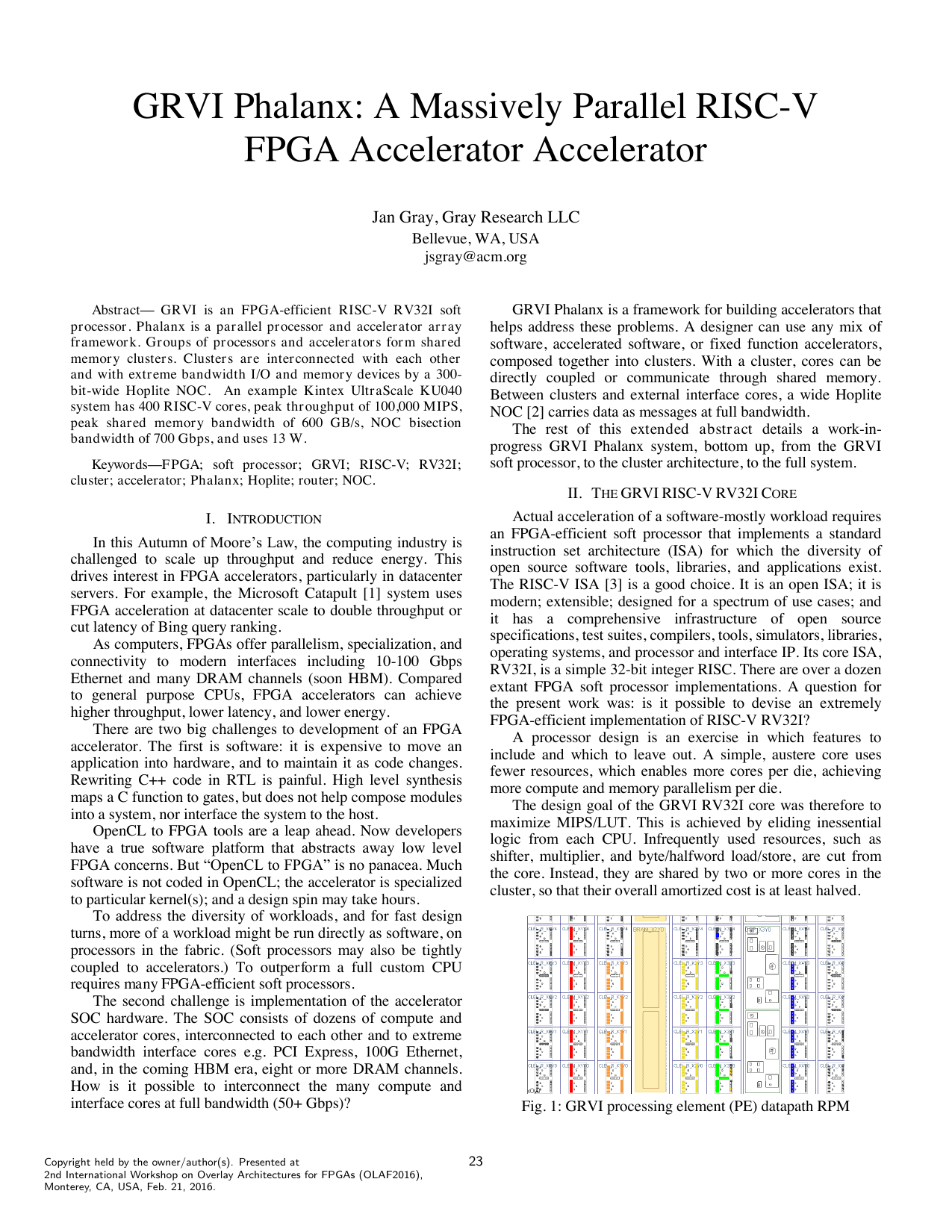
The design goal of the GRVI RV32I core was therefore to maximize MIPS/LUT. This is achieved by eliding inessential logic from each CPU. Infrequently used resources, such as shifter, multiplier, and byte/halfword load/store, are cut from the core. Instead, they are shared by two or more cores in the cluster, so that their overall amortized cost is at least halved. The GRVI microarchitecture is unremarkable. It is a two or three stage pipeline (optional instruction fetch latch; decode; execute). The datapath (Fig. 1) includes a 2R/1W register file; two sets of operand multiplexers (operand selection and result forwarding) and registers; an ALU; a dedicated comparator for conditional branches and SLT (set less than); a PC unit for Ifetch, jumps, and branches; and a result multiplexer to select a result from ALU, return address, load data, optional shift and/or multiply. The color shaded LUTs in Fig. 1, left to right, comprise the register file, first and second operand muxes and registers. ALU, and result multiplexerall 32-bits wide.
The datapath 6-LUTs are explicitly technology mapped and floorplanned into a relationally placed macro (RPM). The ALU, PC unit, and comparator use “carry logic”. Each LUT in the synthesized control unit is scrutinized.
GRVI is small and fast. The datapath uses 250 LUTs; the core overall is typically 320 LUTs. It runs at up to 375 MHz in Kintex UltraScale (-2). Its CPI is not yet determined but is expe
This content is AI-processed based on open access ArXiv data.