The objective of this research was to design a 2.4 GHz class AB Power Amplifier, with 0.18 um SMIC CMOS technology by using Cadence software, for health care applications. The ultimate goal for such application is to minimize the trade-offs between performance and cost, and between performance and low power consumption design. The performance of the power amplifier meets the specification requirements of the desired.
Wireless medical sensor networks have offered significant improvements to the healthcare industry in the 21st century. Devices are arranged on a patient's body and can be used to closely monitor the physiological condition of patients. These medical sensors monitor the patient's vital body parameters, such as temperature, heart rate, blood pressure, oxygen saturation, and transmit the data to a doctor in real time [1]. When a doctor reviews the transmitted sensor readings, they can get a better understanding of a patient's health conditions. The benefit for the patients is that they do not need to frequently visit the hospital, thus patients could reap time and money savings. Such wireless medical sensors will continue to play a central role in the future of modern healthcare. People living in rural areas would especially benefit, since 9% of physicians work in rural areas while almost 20% of the US population lives there [2]. A shortage of physicians and specialist is a big issue in such areas, even today. But Wireless Medical Sensor Network technology has the potential to alleviate the problem.
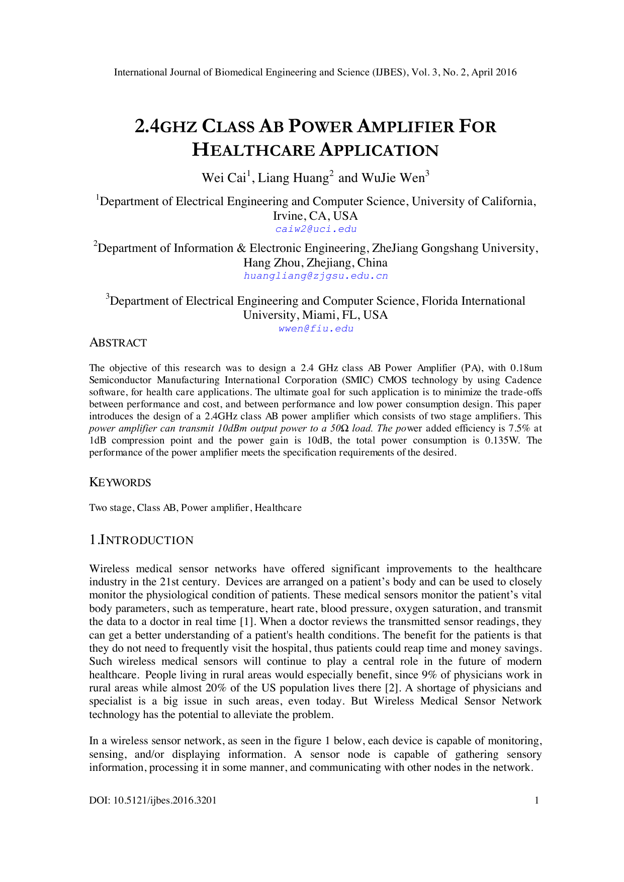
In a wireless sensor network, as seen in the figure 1 below, each device is capable of monitoring, sensing, and/or displaying information. A sensor node is capable of gathering sensory information, processing it in some manner, and communicating with other nodes in the network. Figure 1 shows that the basic sensing node can collect the physiological signals (e.g.: such as EEG, ECG, body temperature, blood pressure, heart beat etc.), when attached to a human body [3]. The processing unit processes all the sensed signals, then sends out the data based on communication protocols. All the processed data will be transmitted through a wireless link to a portable, personal base-station. Doctors can then obtain all the patients’ data through the network.
The main challenge for such sensor node is the high power consumption of portable devices. A solution to this challenge is the integration of the portable devices’ digital and RF circuitry into one chip. The receiver will receive the signal and will also perform DSP processing after the data is sent out by the transmitter [3]. Figure 2 is the transmitter diagram. It is desirable that the transmitter and receiver are low power devices. The director-conversion transmitter is very popular for such applications, because it offers versatility, flexibility, spectral efficiency, and low complexity. These features make the transmitter simpler than the super-heterodyne transmitter. Small chip and circuit size, and low power consumption can be achieved with a direct-conversion transmitter architecture. For the front-end transmitter, the major objectives are 1) transmit RF signals and 2) recover the biosignal classification. This paper proposes a low power receiver design. This paper is mainly for the power amplifier design, since other portions of the circuit design are already discussed in the paper [3]. In order to meet the standards, the PA is designed as shown in table 1.
Over the past 30 years, research on CMOS radio-frequency (RF) front-end circuits has progressed extremely quickly. The ultimate goal for the wireless industry is to minimize the trade-offs between performance and cost, and between performance and low power consumption design [4].
The proposed Class AB amplifier has low output power and good linearity based on the IEEE 802.11b communication protocol. The class AB power amplifier topology is shown in figure 3. The 2.4GHz PA is a two stage common-source amplifier. The first stage is a driver stage, used for providing sufficient driving capability and a proper gain, as seen in figure 4(a), and the second stage is the power output stage which used for performing sufficient output power, as seen in figure 4(b) [5]. For the drive-level circuit, the first design concern was ensuring the input and output conjugate match to different sizes of CMOS transistor. To get the optimum bias, small-signal simulation and 1dB compression point simulation are completed by their power output capability. Resulting design values can be shown in Table 2 and Table3. After the output stage and driver stage, the inter-stage matching circuit is more challenging. If the input of second stage and output of the first stage are all conjugate matched to 50Ω, the two stages can be connected directly. The complete optimized circuit is shown in Figure 5.
As seen in figure 6(a), the gain is 10. As seen in figure 6(b), the frequency is at 2.4 GHz the S11 is less than -10 dB, also, the total power of the PA is 0.135 W.
As seen in figure 7(a), Kf is larger than 1 for all frequencies from 1 to 3 GHz, so this circuit is totally stable. And the PAE is 7.5% at input power 0 dB.
This paper describes the method of designing and simulating power amplifier using cadence software based on SIMC CMOS process 180nm technology. This PA is used for sensor networks. This research is still in the early stages
This content is AI-processed based on open access ArXiv data.