Low-loss phononic integrated circuits based on a silicon nitride-lithium niobate platform
Microwave-frequency acoustic waves in solids have emerged as a versatile platform for both classical and quantum applications. While phononic integrated devices and circuits are being developed on various material platforms, an ideal phononic integra…
Authors: Jun Ji, Joseph G Thomas, Zichen Xi
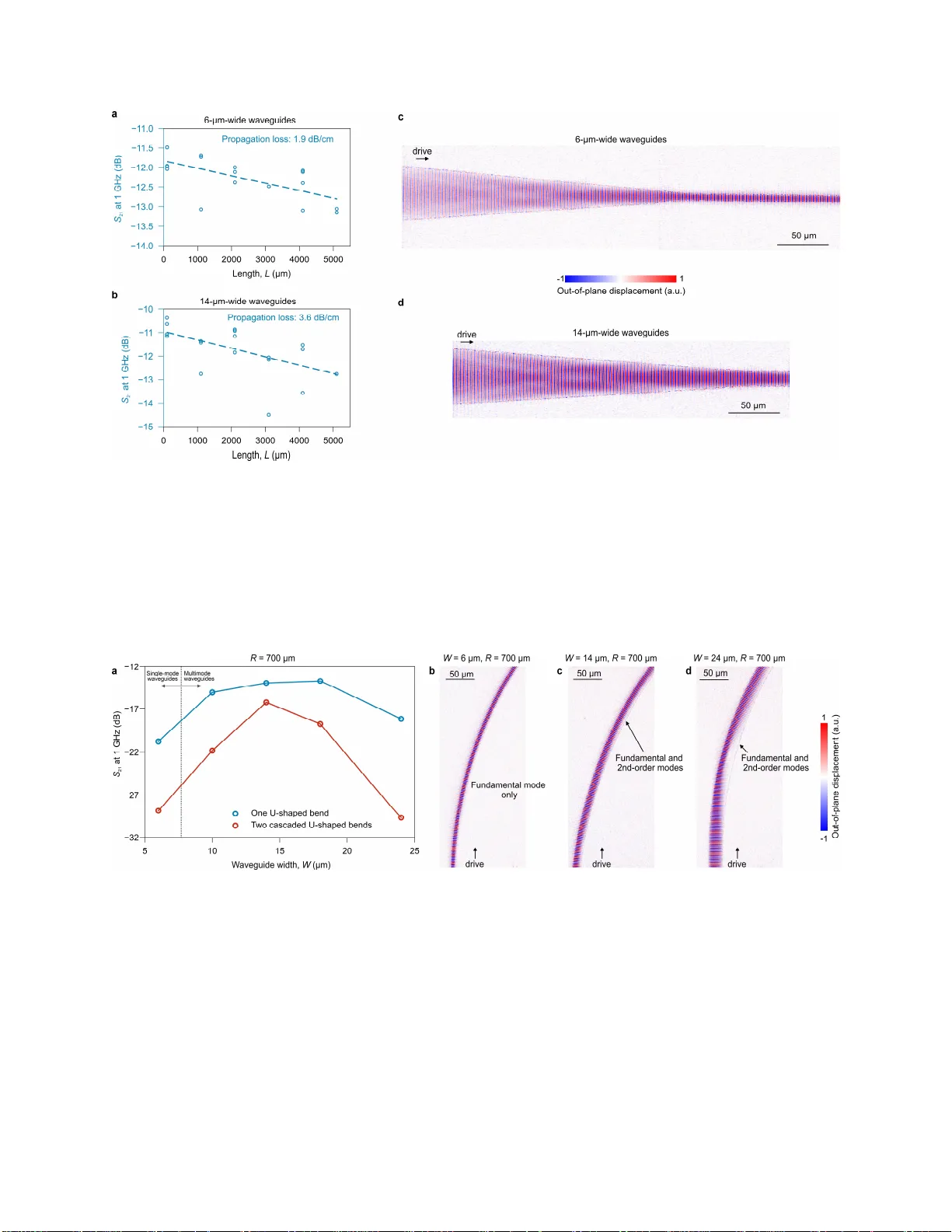
1 Low-loss pho nonic integrated cir cuits bas ed on a silicon nitride-lithium niobate platf orm Jun Ji 1,†,* , Joseph G Thomas 1,† , Zichen Xi 1,† , Ruxuan Liu 2 , Kinson Fang 2 , Yuan Qin 1 , Andreas Beling 2 , Xu Yi 2 , Yizheng Zhu 1 , and Linbo Shao 1,3,* 1 Bradley Department o f Electric and Computer Engineering, Virgin ia Tech, Blacksburg, VA USA 2 Department of Electrica l and Computer En gineering, University o f Virginia, Charlottesvil le, VA, USA 3 Department of Physi cs and Center for Qua ntum In formation Science and E ngineering (VTQ), Virgin ia Tech, Blacksbu rg, VA, USA † J.J., J.G.T., and Z.X. contributed eq ually to this work . * Email: junji@vt.edu ; shaolb@vt.edu Abstract Microwave-frequ ency acoustic waves in solids have emerged as a v ersatile platform for both classical and quantum applications. While phononic integrated devices and circuits are being developed o n variou s material platforms, an ideal phononic integrated circui t (PnIC) platform should simultaneou sly support low- loss waveguide structures, high -quality-factor resonat ors, high-performance mod ulators, and efficient electromechanical transd ucers. Here, we establish a lo w-loss gigahertz-frequen cy PnIC platform based on patterned thin-film silicon nitride (SiN) o n lithium niob ate (LiNbO 3 , LN) sub strate. W e develop low-loss PnIC building blocks including waveguid es, direction al couplers, and high-quality-factor (high- Q ) ring resonators. A s an application , we demonstrate a 1-GHz phono nic oscillator based on a ring reso nator , reaching a lo w phase noise of -159.0 dBc/Hz at a 100-kHz offset fre quency . Our low-loss PnICs could meet the requ irements in micro wave a coustics, quantum phononics, and integrated hybrid systems combining phonons, photon s, superconductin g qubits, and solid -state defects. Introduction Acoustic waves in solids at microwave frequencies have attracted broad attentions for both classical 1-3 and quantum 4,5 applications. Their unique properties of small footprints, long lifetime, and red uced crosstalk are widely exploited in signal processin g 6,7 , sensing 8,9 , compu ting 10,1 1 , and communication 12,13 , makin g them a co mplementary platfo rm to electronics and photon ics. Meanwhile, gigahertz-frequency acou stic waves are envisioned as universal qu antum transducers owing to their efficient coupling to versatile quantum systems, including su perconducting qu bits 14,15 , optical devices 16,17 , and defect cente rs 18,19 . They also show strong potential as more coherent and hardware-efficient quantum memories 20,21 and processors 22 for future quantum net works. Microwave-frequ ency acoustic devices have been primaril y used as discret e components, such as film bulk acoustic resonators (FBA Rs) 23-25 , delay lines 26,27 , and phononic-crystal nanobeam s 28,29 . W ith the surging utility of gigahertz-frequen cy acoustic waves, scaling from di screte devices to large-scale integrated circuits would unlock expanded functionality and superior performance . Moti vated by pho tonic integrated circu its 30-32 that enable large-scale optical computi ng and sensing systems o n chip, phono nic integrated circuits (PnICs) 33 are expected to offer similar capabilities by integrating key building blocks, such as interdi gital transducers (I DT), pho nonic waveguides 34-38 , modulators 39-41 , directional couplers 42,43 , and ring resonators 44-46 , on a single piezoelectric material platform such as gallium nitride (GaN) 43-45,47-49 , lithium niob ate (LN) 46 , and aluminum scandium nitride (AlS cN) 42 . However , their appli cations in microwave engineering and quantum science are h indered by one or more technical challenges including high insertion loss, absence of h igh-frequency- Q -p roduct ( high- fQ ) resonators, or inefficient transd ucers. T hese chall enges could be 2 fully add ressed by sy stematic engin eering of each building block guid ed by a comprehensive understanding of aco ustic-wave device dynamics and loss mechanisms. For example, our in-house optical vibrometer 50 can measure di splacement profile in a high-throug hput manner . In this Article, we establish a low-lo ss gigahertz-frequency PnIC platform based on thin-film silicon nitride (SiN) on LN. By patterning the thin-film SiN layer, we demonstrate low-insertion-loss PnIC building block s at 1 GHz includ ing waveguid es, directional couplers, and hi gh- Q ring resonators. Our acoust ic multimod e (single-mode) wavegu ide features a propagation loss of 3.5 dB/cm (1.9 dB/cm) . Our acoustic taper from wide IDT to waveguide shows a tapering loss of < 1 dB. Our direction al coupler consists of two closely spaced waveguides forming evanescent coupl ing. By adjusting coupling length, we can design power coupling rat es from a 5 0/50 power splitter to a near-comp lete power transfer with an extinction ratio of 2 5 dB. The insertion loss associated with o ur directional co upler is 3.5 dB. Benefiting from our low -loss waveguide and co upler, o ur ring-like resonat or supports a series of high- Q mod es with a free spectral range (FSR) of 0 .4 MHz. Leveraging the 1,001.1 5 MHz aco ustic-wave mo de with a high Q factor o f 17,925 and an insertion loss of 28.2 dB, our acoustic-wave oscillator achi eves a low phase noise of -159.0 dBc/Hz at a 100-kHz offset frequency, surpassing commercial signal generators. We can continuously tune the oscillation frequency from 1, 000 MHz to 1,007 MHz by a combination o f p hase shifter con trol and thermal tuning. Results LN has b een an emerging platform for discrete phononic dev ices fo r th eir re cently developed device fabrication 32 and promisi ng device performances 51 . Scaling discrete devices to integrated circuits, Fig. 1 illustrates the sch ematic of o ur PnICs on a bulk L N substrate with an etched SiN t hin fi lm on top. Surface acoustic wav es (SAWs) are excited by IDT s, then routed by low-loss a coustic waveg uides to interact wit h low-loss directio nal couplers, hig h- Q resonators (e. g., ring reso nators and ph ononic-crystal resonato rs 52 ), Mach-Zehnder interferomet ers, and eventually detected by IDTs. X cut of LN is chosen since it supports both efficient SAW generation via a large electro-me chanical couplin g efficiency k 2 (which is 4.2 % at 1 GHz, details in Supplementary Note 1 ) and strong electro-acoustic mod ulations 39 . Fig. 1: Low–loss phononic integrated circuits usi ng SiN on LN. Schematic of low-loss phononic integrated circuits (PnICs) on a LN substrate (showing green) with a patterned SiN thin film (showing purple) on top. Low-loss SAW building blocks include IDT, waveguides, directional couplers, Mach- Zehnder interferometers, ring r esonators, and phononic-crystal resonators. Dimensions are not scaled. 3 Low-loss phono nic waveguides Low-loss phonon ic waveguides are key elements of PnICs to route phono ns between localized phononic building blocks such as phononic reson ators. Our low- loss acoustic wav eguides ( Fig. 2a ) are defined by opening a slot of width W in th e 3 00-nm-thick SiN thin film on top of bulk L N 39 , with acoustic Ray leigh modes being mo stly confined in LN ( Supplementary Fig. 1 ). Efficient tapering with suppressed scatte ring loss from wide IDTs to narrow waveguides has long been a challenge in PnICs 34,37,42,53,54 . Here, we show that both the orientation of waveguides and the tapering angle θ ( Fig. 2b ) play critical roles in mitigating the scattering loss in the tap er region. On the one hand, o ur acoustic wav eguides are oriented along a 30° an gle with respect to the crystal Z axis, a directio n that exhibits the lowest acoustic ph ase velocity on the X -cut su rface 39 and therefore provides enhanced aco ustic confinement and more efficient tapering. On the other hand, a linear taper with a tapering angle θ ≈ 4.3° enables efficien t transition o f Rayleigh wav e from the wide I DT to th e narrow wavegu ide and vice vers a, as evidenced by the measured out-of-plane displace ment profile ( Fig. 2c ) obtained using our in-house microwave-freq uency optical vibrometer 50 . Under these condi tions, the tapering loss is minimal (< 1 dB) at 1 GHz by comparing S 21 of the tapered waveguide wit h that o f a reference IDT pair ( Fig. 2d ). In contrast, a larger tapering angle of θ ≈ 9.4° induces a significant tapering loss of 1 3 dB ( Supplementary Fig. 2 ). We characterize the propagation loss of a coustic waveguides by measuring S 21 of straight waveguides with lengths L ranging from 100 μ m to 5 100 μ m. For large wavegu ide wid ths such as W = 1 0 μ m ( Fig. 2e ) and W = 14 μ m ( Supplementa ry Fi g. 3 ), high- order mod es are supp orted ( Supplementary Fig. 1 ), and the propagation loss of these multimode waveguides is around 3.5 dB/cm. F or small wav eguide widths such as W = 6 μ m, only the fundamental mode is supported ( Supplement ary F ig. 1 ), and the propagatio n loss of Fig. 2: Low-loss acoust ic w aveguides. (a) O ptical micrograph of the fabricated acoustic w aveguide with a waveguide width of W and a length of L . (b) Scanning electron microscopy (SEM) images of the tapering transition bet ween the IDT and the waveguide with a tapering angle of θ . (c) Measured out-of-plane displacement profile at the tapering region using our in-house op tical vibrometer. (d) M easured transmission spectrum S 21 of our acoustic waveguide with W =10 μm and L = 100 μm , compared with that of a reference IDT p air. (e) Extracted propagation loss of 10- μm -wide acoustic waveguides based on transmission spectra S 21 as a function of the waveguide length L . (f,h) Optical micrograph of a coustic waveguides with one U- shape b end and two cascaded U-shape bends, respectively. (g) M easured out-of-plane displacement profile at the b ending region for a bending radius R = 300 μm , showing strong acoustic wave leakage. (i,j) Measured out-of-plane displacement profiles for waveguides with a larg er bending radius R =1300 μm , demonstrating suppressed leak age. (k) Propagation loss of 10- μm -wide bent acoustic waveguides as a function of bending radii R . The color scale is independently normalized for (c) , (g) , and (i-j) . 4 the single-mode waveguide is as low as 1.9 dB/cm ( Supplementary Fig. 3 ). The lower p ropagation loss from the single-mode w aveguide is attribu ted to two factors. On the o ne hand, the fun damental mode profile is mostly confined in th e center of LN, leading to less scattering lo ss from the interaction between the modes and the rou gh sidewalls of SiN. On the o ther hand, th e single-mode wav eguide proh ibits surface-roug hness- induced or defect-ind uced mo de conv ersions from the fundamental even mode to high-order odd mo des that canno t be detected by the IDT. Our acoustic waveguide is featured with a low pro pagation loss, comparable to that of the state-of-th e-art acoustic rib wav eguides ( Ta ble 1 ). Table 1 Comparisons of key performance metrics for different compet ing acoustic waveguide platforms at room temperature. Platform Waveguide group vel ocity (km/s) Propagation loss (dB/cm) Insertion loss* (dB) SiN on LN (this work) 3.4 3.5 (Multimode waveguides at 1 GHz) 1.9 (Single - mode waveguides at 1 GHz ) ~10 ( L = 100 μm, 1.0 GHz) GaN-on-sapphire 44 4.18 0.5 (0.2 GHz) 12.5 (scaled to 1 GHz) >70 (100 MHz) GaN-on-SiC 45 3.76 36 (3.4 GHz) 3.1 (scaled to 1 GHz) 38 ( L = 4100 μm, 3.4 GHz) 23.6 ( L scaled to 100 μm, 3.4 GHz) LN - on - diamond 36 2.8 _ 21 ( L = 100 μm, 2.8 GHz) AlScN-on-SiC 37 6.48 107 at 4.05 GHz 6.5 scaled to 1 GHz ~ 30 ( L = 320 μm, 4.05 GHz) AlScN-on-SiC 42 5.05 16.1 (2.1 GHz) 3.65 (scaled to 1 GHz) 32 ( L = 160 μm, 2.1 GHz) * Insertion loss, here, is defined as S 21 between two electrical ports of acoustic waveguides. We extract the propag ation loss of bent acoustic waveg uides by subtracting the measured S 21 of one U- shape bend ( Fig . 2f ) and two cascaded U-sh ape bends ( Fig. 2 h ). F or a fixed waveguide width of 10 μm, t he propagation loss of ben t acoustic waveguides is reduced sig nificantly fro m 176.5 d B/cm to 6.5 dB/cm and approaches to that of the straight waveguide, as the bend ing radius increases from 300 μ m to 1300 μ m ( Fig. 2k ). At a s mall bending radius such as R = 30 0 μ m ( Fig. 2g ), significant acoustic wave leakage is observed from the out-of- plane displacement pro files. Acoustic power in fundamental mod e is significantly coupled to the 2 nd-order mode in the bent section and then inefficiently coupled back to the fund amental mode at the very end of th e bend . At a l arge bend ing rad ius such as R = 1 300 μ m ( Figs. 2 i and 2 j ), the coup ling to the 2nd-o rder mode is supp ressed througho ut the propag ation in the b ending section (so -called adi abatic bend 55 in the integrated photo nic waveguides) and a better confinemen t is observed. For a fixed waveguide radius of 700 μm, we observed an optimal wavegu ide width of 14 μm with a minimum propagation loss ( Supplementary Fig. 4 ). This is likely a matched bend case 55,56 which h as been well-kn own in int egrated photonic waveguides. In this case ( Suppl ementary Fig. 4c ), the phase of the fundamental and 2nd-order modes return in ph ase after the propagation in the b ent section, and thu s acoustic power is efficiently coupled back to the fundamental mode at the very end of t he bend 56 . Low-loss phono nic directional couplers Phononic directional couplers ar e essential devices for splitting and combin ing acoustic waves in phononic systems. Based on our low-loss acoustic waveguides, we demonstrate low- loss phononic directional coupler with co ntrollable power transfer ( Fig. 3a ). Our di rectional co upler consists of two evanescently coupled waveguides, with a co upling g ap G c and a coupling len gth L c ( Fig. 3b ). With a fixed G c of 2 μm and adjusting the co upling length, we demonstrate controlled power transfer ( Fig. 3c ) from the input port (P1) 5 to the throug h port (P2) and drop port (P3). At a coup ling length o f 100 μm, we o btain a 50/5 0 power splitter with an insertion loss of 6 .5 dB from th e coupler and 10 d B loss from IDT pair at each ou tput port . In this case, the measured o ut-of-plane disp lacement profile at the through port and d rop port have a similar magnitude ( Fig. 3d ). At a coupling length of 300 μm, we have a near-complete power transfer to the drop port with an insertio n loss of 3 .5 dB associated with the coupler and an extinction ratio of 25 dB between two output ports, wh ich is also confirmed b y measured o ut-of-plane displ acement profile ( F ig. 3e ). High- Q and low -insertion-loss phononic ring reson ators High- Q pho nonic resonators are essential for PnIC in applicat ions such as signal generatio n 57,58 , signal processing 59,60 , and sensing 8,44 . Our resonator consists of a ring-like structure evanescently coupled to two waveguides ( Fig. 4a ). The wid ths of waveguides and the ring are chosen as 14 μ m to minimize propagati on loss. Benefi ting from low tapering lo ss and low prop agation loss of o ur waveg uide, the ring resonator supports a series of high- Q acoustic modes. For a rin g radius of R = 1300 μ m, th ese modes are spectrally spaced at a FSR o f 0.403 MHz ( Fig. 4b ) at a group velo city v g of 3 ,400 m/s. The mode at f 0 = 1001.15 M Hz simultaneously featu res a high loaded Q factor of 17,92 5 and an insertion loss (from cable t o cable) of - 28.2 d B ( Fig. 4c ) b etween the input p ort (P 1) and the drop port (P3). We extract the intrinsic Q factor Q in and the co upling Q facto r Q c (per coup ler) using temporal coupled mode theo ry (details in Supplementary Note 2 ). With a coup ling gap G c = 2 μm an d a coupling length L c = 100 μm, our ring resonator operates in the under-coupled regime with Q in = 20,436 and Q c = 291,743. The correspon ding propagation lo ss rate per unit l ength, inferred from Q in , is estimated as α = 2π f 0 /( v g Q in ) = 3.9 d B/cm, which is consistent with the propagation loss ex tracted from the waveguide measu rements ( Supplementary Fig. 3 b ). Low-phase-no ise phononic oscill ators Based on our high- Q and low-insertion-loss ring resonator, we demonstrate a low -phase-noise phononic oscillator for microwave signal generation. A p ositive feedback loop is implem ented ( Fig . 4d , details in Methods - Device charac terizations ) between the inp ut p ort and th e d rop port of the reson ator, in which the losses are fully compensated by the gain o f a low- noise amplifier (LNA). We tune the phase shifter in the loop such that the phase delay withi n the loop at 1001.15 MHz is an integer mu ltiple of 2π and self - oscillation is sustain ed. The signal of our o scillator at a level of 5.6 d Bm is coupled ou t from the coupler, and its ph ase no ise is directly measured usin g a phase noise analyzer ( Fig. 4e ). For comparison, th e phase Fig. 3: Low- loss acoustic directional couplers. (a) Optical micrograph of the fabricated acoustic directional coupler on lithium niobate. (b) Close-up view of the coupling region, showing the coupling gap G c and coupling length L c . (c) M easured transmission S 21 ( S 31 ) at 1 GHz for the through ( drop) port P2 (P3), as a fun ction of coupling length L c , demonstr ating controllable p ower transfer between the two waveguides. (d) Measured out-of- plane displacement profile of a 50/50 directional coupler, where acoustic p ower is equally split bet ween the through and drop ports. (e) Measured out-of-plane displacement profile of a strongly coupled (near -complete power-transfer) directional coupler, where most of the acoustic power is tran sferred to the drop port. The color scale is independently normalized for (d–e) . 6 noise spectra of two commercial sig nal generato rs (Rigol DSG836A and Keysight N5 183B equipped with the low-phase-n oise option UNY) at 1 G Hz carrier freq uency are prov ided for comparison. At a 1- kHz (1 0-kHz) offset frequency , t he ph ase noise of our oscillator reach es - 106.3 dBc/Hz (-138.4 dBc/Hz), representing an improvement of 9.5 dB (22.3 dB) over the Rigol signal g enerator. At these low offset freque ncies, the me asured ph ase no ise exhibi ts a -30 dB/d ecade slope, wh ich is mainly attributed to the temperat ure fluctuat ion Δ T 8 . Compared with oscillators based on phononic-crystal resonators 57 and acoustic delay lines 61 , our rin g resonator possesses a larger acoustic mode volume V , leading to a larg er heat capa city C = C p × ρ × V , and co nsequently reduced temperature fluctuation Δ T = / . Here, C p is the heat ca pacity at constant pressure of L N, ρ is the density of LN, k B is the Boltzman n constan t, and T is th e env ironmental temperature . Wit h in jection locking, the phase noise at low offset frequencies (< 1 kHz) could be further suppressed without affecting the no ise performance at larg er offset freq uencies 62 . At larger offset frequen cies, our oscillator achieves an ultralow noise floor of -159.0 dBc/Hz at a 100-kHz offset frequency, which is 13 dB lower than that of the Keysight signal generator. In this regime, the phase noise is dominated by the background thermal noise at the LNA inpu t. Reducing the reson ator inserti on loss would allow operation with lower amplifier g ain to reach osci llation threshold, thereby reducin g Fig. 4: High- Q and low-insertion-loss acoustic ring resonators and low -phase-noise o scillators. (a) Optical micrograph of the fabricated four -port ring-like resonator with a radius of R and a coupling length of L c . (b) Measured transmission s pectrum S 31 of our ri ng resonator with R = 1300 μm and L c = 100 μm . High- Q modes are spectrally spaced at a free spe ctral range (FSR) of 0.43 MHz. (c) Close-up view of the measured (dots) and fitted (solid line ) S 31 of the mode with the lowest insertion l oss. Th is mode is centered at 1001.15 MHz with a full w idth at half maximum (FWHM) of 55.85 kHz, resulting in a loaded qu ality ( Q ) factor of 17,925. (d) Experimental setup used to build and characterize our acoustic ring oscillator. Our oscillator consists of the ring resonator, a low noise amplifier (LNA), an attenuator, a microwave phase shifter and a microwave power coupler. T h e oscillator outputs from the coupling port of the coupler are measured by a phase noise analyzer. (e) Measured phase noises of our acoustic ring oscillator, compared with those from Rigol signal generator DSG836A and Keysight sign al generator N5183B with the low-phase-noise option. ( f ) Continuous tuning of the oscillation frequency from 1,000 MHz to 1,007 MHz through a combination of voltage-controlled phase shifter and thermal tuning of the oscillator by 18 °C. 7 amplified thermal noise and further lowering the noise floo r. To the best of our kno wledge, this device exhibits the lowest reported phase noise among ph ononic oscil lators at 1-kHz, 10-kHz, and 100- kHz offsets ( Table 2 ). Recent photonic micro wave-generatio n platforms 63-65 demo nstrate approximately 2 0 dB lower phase noise at 10-kHz offset (scaled to 1 GHz). Ho wever, th eir large footprint, high power consumption, and high system co mplexity n ecessitate further develo pments for practical deployment. Furthermore, continuously tunin g the oscillation frequency of our oscillato r from 1,000 MHz to 1, 007 MHz ( Fig. 4f ) is realized by a combination of voltage-controlled phase shifter and thermal tuning of the oscillator by 18 °C (details in Methods - Dev ice characterizati ons ). Table 2 Comparisons of phase noise of different acoustic oscillator desi gns. Reference Platform Acoustic Mode Frequency (MHz) Insertion loss* (dB) Phase noise (dBc/ Hz) 1 kHz offset 10 kHz offset 100 kHz offset This work SiN on LN Rayleigh 1,00 1.2 28.2 - 106.3 - 106.3 - 138.4 - 138.4 - 159.0 - 159.0 57 LN Rayleigh 1026 20 -102.0 -102.2 -132.5 -132.7 - 140.0** -140.2 67 LNOS SH - SAW 888.6 5.2 - 94.1 - 93.1 - 117.5 - 116.5 - 139.2 - 138.2 68 ZnO on diamond Sezawa 1008 9.0 - 90.0** -90.1 -118.0** -118.1 - 137.0 * * -137.1 61 LN SH 0 157 3.2 - 101 - 84.9 - 127 - 110.9 - - 69 C rystal - 26 - - 138 - 106.3 - 154 - 122.3 - 159 - 127.3 70 Silicon BAW 103.4 - - 108 - 88.3 - 120** - 100.3 - 130** - 110.3 71 InGaAs on LN # Rayleigh 999 25** -5 7 -57 -82** -82 -110* -110 The values in the shaded cells are scaled to a 1 GHz carrier. * Insertion loss, here, is defined as S 21 between two electrical ports of acoustic resonators. **Data extracted from figures. # This device has solid-state in-cavity gain. Table 3 Building blocks of our integrated phononic circuit. C omponent Spec ifications Insertion loss * at 1 GHz (dB) IDT Pair The IDT finger pitch is 1.651 μm ; the IDT wi dth is 50 μm ; the thickness of aluminum is 100 nm; the number of IDT pairs is 35 . 10 IDT - Waveguide tapering θ ≈ 9.4 ° <1 Waveguides L = 0 .1 mm , W = 10 μ m 0.4 Directional coupler W = 10 μm, G = 2 μm 13.5-10 = 3.5 between the input and drop ports Ring resonator W = 14 μm, R = 1300 μm 28.2-10 = 18.2 between the input and drop ports * Insertion loss, here, is defined as S 21 between two ports of each acoustic component. Discussion We demonstrate a low–l oss Pn ICs platform using SiN on LN. Low-in sertion-loss SAW bu ilding blocks such as waveguides, directional couplers, and evan escently coupled high- Q ring reson ators are realiz ed ( Table 3 ). Building up on the ring resonator , we furth er demonstrate a 1-GHz SA W oscillator with an ultralow phase no ise of -159.0 dBc/Hz at a 100- kHz offset frequency . Our acoustic waveguide could be scaled towards sub-terahertz frequencies ( Supplementary Fig. 5 ) through engineering of the waveguide o pening width and the deposited SiN fil m t hickness. Importantly, our slot- waveguide-based circuit architecture i s implemented on a bulk piezoel ectric substrate, mai ntaining propagation loss comparable to those of acoustic rib waveguides, while eliminating the need s to develop 8 thin-film t echnologies 36,66 and special ized etching processes for piezoelectri c materials. This approach ma y facilitate the application of our circuit architectu re to emerg ing material platforms (e.g., po tassium niobate.) which o ften lack sophisticated nanofab rication technologies. Moreover, our SiN-on-LN platform could be compatible with phot onic in tegrated circuits, facilitating co -integration with other optical, electro-o ptic, acousto-optic componen ts to fo rm l arge-scale hybrid integrated systems for ap plications in microwave signal processing, sensing, and t erahertz technologies. Methods Device design and fabrication The device is on a X -cut LN substrate with a SiN thin film deposited on top. The pitch of IDT fingers is 1.651 μm , which corresponds to the half wavelength of acoustic wave at 1.005 GHz. The width of the IDT is 50 μm. The thickness of aluminum is 100 nm. The number of I DT pairs is 35. A 300-nm-thick SiN l ayer is deposited u sing plasma-enhanced chemical vapor deposition on the X -cut LN substrate. The SiN layer is patterned u sing electron-beam lithography (EBL) with a 900-nm-th ick polymethyl methacrylate (PMMA) resist and etched using r eactive -ion etch ing with carbon tetrafluoride, sulfur hexafluoride and trifluoromethane gases. The metal layer is p atterned using EBL with a 300-nm-thick PMMA resist. A 100-nm-thick aluminium layer is deposit ed using electr on-beam evaporation, followed by lift-off in N-Methyl-2-pyrrolidone (NMP). Device characteriza tions The S -parameter spectra measurements are conducted using a Vector Network Analyzer (Keysight P500 0A) . The positive feedback loop of SAW oscillation consists of our acoustic resonator, a LNA (Mini -circuits, ZKL-33ULN- S+), a phase shifter (RF LAMBDARFPSHT0002W1), a 3-dB attenuator, and a coupler (M ini-circuits, ZFDC10-5- S+). The signal of our oscillator is coupled out from the coupler, and the corresponding phase noise is directly measured using a phase noise analyzer (R&S FSWP). For the tuning of the oscillation frequency , we use a voltage- controlled phase shifter (Mini-circu its, JSPHS -1000) and a temperature-controlled sample stage. The temperature- controlled sample stage uses a K -style temperature sensor an d a 6 .8- Ω 25 -W power resistor (CGS HSA256R8). The temperature sensor is read out by a multimeter (F luke 45), whereas th e power resistor is powered by a d.c. power supply (RIGOL DP832A). A proportional–integral–derivative control algorithm in Python is used to stabilize the temperature. Acknowledgements Funding: Device fabrication was conducted at the Center for Nanophase Materials Sciences (CNMS2022 -B-01473, CNMS2024-B-02643), which is a US D epartment of Energy Office of Science User Facility. Research was partially supported by the Air Force O ffice of Scientific Research (AFOSR) under Grant Number W911NF -23-1-0235 and Award Number FA9550-22-1-0548, and by Commonwealth C ybersecurity Initiative in Virginia. Devel opment of the optical vibrometer was partially supported by the Defense Advanced Research Projects Agency (DARPA) OPTIM program under contract HR00112320031. Dev elopment of the phononic device was partially supported by D ARPA SynQuaNon DO program under Agreement HR00112490314. Measurements of the phase noise were partially supported b y DARP A GR YPHON program under Agreement HR001 12220008. The views and conclusions contained in this document are those o f the authors and do not necessarily reflect the position or the policy of the United States Government. No official endorsement should be inferre d. Approved for public release. Author contributions: J.J., J.G.T., and Z.X. con tributed equally to this work. J.J. designed the chip with the help o f L.S. J.J. fabricated the devices with the help from L.S., Z.X., and Y.Q. J.J. and Z.X. performed the measure ments and analyzed the data. Z.X., J.J., R.L., K.F., A.B., X.Y, and L.S. performed phase noise measurements. J.G.T. and Y .Z. performed optical vibrometer measurements. All au thors analyzed and interpreted the results. J.J. prepared the manuscript with revisions from all authors. L.S. supervised the project. Competing interests: The authors declare that they have no competing i nterests. Data availability: All data needed to evaluate the conclusions in the paper are present in the paper and/or the Supplementary Materials. Additional data related to this paper ma y be requested from the authors. 9 References 1 Hashimoto, K.-y . RF bulk acoustic wave filters for communications . (Artech House, 2009). 2 Gong, S., Lu, R., Y ang, Y ., Gao, L. & H assanien, A.E. Microwave Acoustic D evices: Recent Advances an d Outlook. IEEE Journal of Micr owaves 1 , 601-609 (2021). 3 Priya, P ., Cardozo de Oliveira, E. & Lanzillotti-K imura, N.D. Per spectives on high -frequency nanomechanics, nanoacoustics, and nanophononics. Applied Physics Letters 122 , 140501 (2023). 4 Delsing, P . et al. The 2019 surface acoustic w aves roadmap. Journal of Physics D: Applied Ph ysics 52 , 353001 (2019). 5 Chu, Y . & Gröblacher , S. A perspective on h ybrid quantum opto - and electromechanical systems. Applied Physics Letters 1 17 , 150503 (2020). 6 Y ang, Y ., Lu, R., Gao, L. & Gong, S. 4.5 GHz lithium niobate MEMS filters with 10% fractional bandwi dth for 5G front-ends. Journal of Micr oelectro mechanical Systems 28 , 575-577 (2019). 7 Giribaldi, G., Co lombo, L. , Simeoni, P . & Ri n aldi, M. C ompact a n d wideband nanoacoustic pass -band fi lters for future 5G and 6G cellular radios. Natur e Communications 15 , 304 (2024). 8 Xi, Z. et al. Room-T emperature Mid-Infrared Detection Using Metasurface-Absorber-Integrated Phononic Crystal Oscillator . Laser & Photonics Reviews 19 , e00498 (2025). 9 Lin, B. et a l. A high Q value ScAlN/AlN-based SA W resonator for load sensing. IEEE T ransactions on Electr on Devices 68 , 5192-5197 (2021). 10 Ji, J. et al. Synthetic-domain computing and n eural networks u sing lithium n iobate integrated nonlinear phononics. Natur e Electro nics 8 , 698-708 (2025). 1 1 Zhao, H., Li, B., Li, H. & Li, M. Enabling scalable optical computing in synthetic frequency dimensi on using integrated cavity acousto-optics. Natur e Communications 13 , 5426 (2022). 12 Hays, R.M. & Hartmann, C.S. Surface-acoustic-wave devi ces for c ommunications. Pr oceedings of the IEEE 64 , 652-671 (1976). 13 Manzaneque, T ., Lu, R., Y ang, Y . & Gong, S. in 2017 Joint Confer ence of the European Frequency and T ime Forum and IEEE International Fr equency Contr ol Symposium (EFTF/IFCS). 143-147 (IEEE). 14 O’Connell, A.D. et al. Quantum ground state and single-phonon control o f a mechanical resonator . Nature 464 , 697-703 (2010). 15 Chu, Y . et al. Quantum acoustics with superconducting qubits. Science 358 , 199-202 (2017). 16 Aspelmeyer , M., Meystre, P . & Schwab, K. Quantum optomechanics. Physics T oday 65 , 29-35 (2012). 17 Aspelmeyer , M., Kippenber g, T .J. & Marquardt, F . Cavity optomechanics. Reviews of Modern Physics 86 , 1391-1452 (2014). 18 Meesala, S. et al. Strain engineering of the silicon-vacancy center in diamond. Physical Review B: Condensed Matter 97 , 205444 (2018). 19 Whiteley , S.J. et al. Spin–phonon interactions in silicon carbide addressed by Gaussian acoustics. Nature Physics 15 , 490-495 (2019). 20 Pechal, M., Arrangoiz-Arriola, P . & Safavi-Naeini, A.H. Superconducting circuit quantum computing with nanomechanical resonators as storage. Quantum Science and T echnology 4 , 015006 (2018). 21 Hann, C.T . et al. Hardware-Efficient Quantum Random A ccess Memory with Hybrid Quantum Acoustic Systems. Physical Review Letters 123 , 250501 (2019). 22 Qiao, H. et al. Splitting phonons: Building a platform for linear mechanical quantum computing. Science 380 , 1030-1033 (2023). 23 W ang, J. et al. A Film Bulk Acoustic Resonator Based on Ferroelectric Aluminum Scandium Nitride Films. Journal of Micr oelectromech anical Systems 29 , 741-747 (2020). 24 Y ang , Y ., Lu, R., Manzaneque, T . & Gong, S. in 2018 IEEE International Fr equency Contr ol Symposium. (IEEE). 25 Zou, Y . et al. Aluminum scandium nitride thin-film bulk acoustic resonators for 5G wideband applications. Micr osystems & Nanoengineering 8 , 124 (2022). 26 Lu, R., Y ang, Y ., Li, M.H., Breen, M. & Gong, S. 5 -GHz Antisymmetric Mode Acoustic Delay Lines in Lithium Niobate Thin Film. IEEE T ransactions on Micr owave Theory and T echniques 68 , 573-589 (2020). 27 Lu, R., Manzaneque, T ., Y ang, Y ., Li, M.-H. & Gong, S . Gigahertz low -loss and w ideband S0 mode lithium niobate acoustic delay lines. IEEE transactions on ultrasonics, ferr oelectrics, and fr equency contr ol 66 , 1373-1386 (2019). 10 28 Kalaee, M. et a l. Quantum electromechanics of a hypersonic crystal. Natur e Nanotechnology 14 , 334-339 (2019). 29 MacCabe, G.S. et al. Nano-acoustic resonator with ultralong phonon lifetime. Science 370 , 840-843 (2020). 30 Jalali , B. & Fathpour , S. Silicon Photonics. Journal of Lightwave T echnology 24 , 4600-4615 (2006). 31 Moss, D.J., Morandotti, R., Gaeta, A.L. & Lipson, M. New CMOS -compatible platforms based on silicon nitride and Hydex for nonlinear optics. Natur e Photonics 7 , 597-607 (2013). 32 Zhu, D. et a l. Integrated photonics on thin-f ilm lithium niobate. Advances in Optics and Photonics 13 , 242- 352 (2021). 33 C. Balram, K. Piezoelectric phononic integrated circuits. Applied Physics Letters 125 , 200505 (2024). 34 Ding, S.W . et al. Integrated phononic waveguides in diamond. Physical Review Ap plied 21 , 014034 (2024). 35 Lee, J., W ang, Y ., Zorman, C.A. & Feng, P .X. -L. 3C-SiC phononic waveguide for manipulating mechanical wave propagation. Journal of Ap plied Physics 135 , 204501 (2024). 36 Malik, S. et al. Integrated phononic waveguide on thin-film lithium niobate on diamond. Applied Physics Letters 127 , 154001 (2025). 37 Deng, Y . et al. Monolithic AlScN/SiC phononic w aveguides for scalable acoustoelectric and quantum devices. APL Materials 13 , 101 107 (2025). 38 Guida, J. & Ghosh, S. Design and an alysis of guided surface acoustic waves in ScAlN on sapphire for phononic integrated circuits. IEEE T ransactions on Ultrasonics, Ferr oelectrics, and Fr equency Contr ol 72 , 44-54 (2024). 39 Shao, L. et al. Electrical control of surface acoustic waves. Nat. Electr o n. 5 , 348–355 (2022). 40 Shao, L. et al. Th ermal Modulation of G igahertz Surface Acoustic W aves on Lithium Niobate. Physical Review Applied 18 , 054078 (202 2). 41 Shao, S., Luo, Z. & W u, T . Electro -acoustic p hase modulator based on AlScN thin film. IEEE Electr on Device Letters 44 , 817-820 (2023). 42 Guida, J. & Ghosh, S. Phononic Integrated Circuit Component Design and Analysis for Surface Acoustic W aves in ScAlN on Silicon Carbide. Journal of Micr oelectr omechanical Systems 34 , 368-378 (2025). 43 Xu, X.-B. et al. Gigahertz top ological phononic circuits bas ed on micrometre-scale unsuspended waveguide arrays. Natur e Electronics 8 , 689–697 (20 25). 44 Fu, W . et a l. Phononic integrated circuitry and spin –orbit interaction of phonons. Natur e Communications 10 , 2743 (2019). 45 Bicer , M. & Balram, K.C. Low -Loss GHz Frequency Phononic Integrated Circuits in Gallium Nitride for Compact Radio Frequency Acoustic W ave Devices. IEEE T ransactions on Ultrasonics, Ferr o electrics, and Fr equency Control 71 , 172-181 (2024). 46 Mayor , F .M. et al. Gigahertz Phononic Integrated Circuits on Thin-Film Lithium Niobate on Sapphire. Physical Review Applied 15 , 014039 (2021). 47 Bicer , M., V alle, S., Brown, J., Kuball, M. & C. Balram, K. Gallium n itride ph ononic integ rated circ uits platform for GHz frequency acoustic wave devices. Applied Physics Letters 120 , 243502 (2022). 48 Feng, Z., Liu, Y ., Xi, X., W ang, L. & Sun, X. Gigahertz Phononic Integrated Circ uits Based on Overla y Slot W aveguides. Physical Review Applied 19 , 064076 (2023). 49 Xu, X.-B. et al. Large-scale programmable phononic integrated circuits. arXiv preprint (2025). 50 Thomas, J.G. et al. Spectral interferometry-based microwave-frequency vibrometry for integrated acoustic wave devices. Optica 12 , 935-944 (2025). 51 Lu, R. & Gong, S. RF acoustic microsystems based on su spended lithium niobate thin films: advances a nd outlook. Journal of Micr omechanics and Micr o engineering 31 , 1 14001 (2021). 52 Ji, J. et al. On-chip cavity electro-acoustics using lithium niobate phononi c crystal resonators. arXiv pr eprint arXiv:2510.27496 (2025). 53 Dahmani, Y .D., Sarabalis, C.J., Jiang, W ., Mayor , F .M. & Safavi-Naeini, A.H. Piezoelectric T ransduction of a W avelength-Scale Mechanical W av eguide. Physical Review Applied 13 , 024069 (2020). 54 Lee, D. et al. Direct V isualization of Gi gahertz Acoustic W ave Propagation in Su spended Phononic Circuits. Physical Review Applied 16 , 034047 (2021). 55 Cherchi, M., Ylinen, S., Harjanne, M., Kapulainen, M. & Aalto, T . Dramatic size reduction of wavegui de bends on a micron-scale silicon photonic platform. Optics Expr ess 21 , 17814-17823 (2013). 56 Melloni, A., Monguzzi, P ., Co sta, R. & Martinelli, M. Design of curved waveguides: the matched bend. Journal of the Optical Society of A merica A 20 , 130-137 (2003). 1 1 57 Xi, Z. et al. Low-phase-noise surface-acoustic-wave oscillator u sing an edge mode of a phononic band gap. Physical Review Applied 23 , 024054 (2025). 58 Kourani, A., Y ang, Y . & Gong, S. L- and X-Band D ual-Frequency Synthesizer U tilizing Lithium Niobate RF - MEMS and Open-Loop Frequency Dividers. IEEE T ran sactions on Ultrasonics, Ferr oelectrics, and Fr equency Control 68 , 1994-2004 (2021). 59 T urner , P . et al. 5 GHz band n79 wideband microacoustic filter using thin lithium niobate membrane. Electr onics letters 55 , 942-944 (2019). 60 Zhang, L., Cu i, C., Xue, Y ., Chen, P . & Fan, L. Scalable photonic -phonoinc integrated circuitry for reconfigurable signal processing. Natur e Communications 16 , 2718 (2025). 61 Li, M.-H., Lu, R., Manzaneque, T . & Gong, S. Low Phase N oise RF Oscillators B ased on Thin -Film Lithium Niobate A coustic Delay Lines. Journal of Micr oelectr o mechanical Systems 29 , 129-131 (2020). 62 Xi, Z. et al. Injection Locking of Gigahertz - Frequency Surface Acoustic W ave Phononic Crystal Oscillator . physica status solidi (a) 223 , e202500605 (2026). 63 Kudelin, I. et al . Photonic chip-based low-noise microwave oscillator . Natur e 627 , 534-539 (2024). 64 Sun, S. et al. I ntegrated optical f requency division for microwave and mmW ave generation. N atur e 627 , 5 40- 545 (2024). 65 He, Y . et al. Chip-scale high-performance photonic microwave oscillator . Science Advances 10 , eado9570 (2024). 66 Zulu, T .S. et al. Heterogeneous T ransfer of Thin Film BaT iO3 on to Silicon for Device Fabrication. arXiv pr eprint arXiv:2601.14551 (2026). 67 Chang, C.Y ., Y u, Y .C., Lee, Z.Q. & Li, M.H. A V oltage -Controlled Surface Ac oustic W ave Oscillator Based on Lithium Niobate on Sapphire Low-Loss Acoustic Delay Line. IEEE T ransactions on Ultrasonics, Ferr oelectrics, and Fre quency Contr ol 71 , 1314-1323 (2024). 68 Prechtel, V . et al. in IEEE Ultrasonics Symposium, 2004. 199-202 (IEEE). 69 T sai, M.-D. et al. in 2008 IEEE Radio Fr equency Integrated Cir cuits Symposium. 533-536 (IEEE). 70 Sundaresan, K., Ho, G.K., Pourkamali, S. & A yazi, F . in IEEE Custom Integrated Cir cuits Confer ence 2006. 841-844 (IEEE). 71 W endt, A. et al. An electrically injected solid-state s urface acoustic wave p honon laser . Nature 649 , 597-603 (2026). 12 Supplementary Note 1. k 2 simulation The electromechanical couplin g coefficien t is calculated from the phase velocity difference between the cases where the bo undary condition at the IDT coupler surface is electrical ly free or shorted: = 2( − )/ A large 2 means h igher conversion efficiency between electrical and acoustic energy in a piezoel ectric material. According to our simulations, = 338 8.9 m/s and = 3317.2 m/s, leading to a k 2 of 4.2%. Supplementary Note 2. Temporal coupled-mode theory for acoustic ring resonators Assuming a circulati ng fiel d ampli tude A in the resonator and S i in the waveguide p ort (Pi) ( Fig. 4a ). Specifically, S 1 is the input port (P1), S 2 is the through port (P2), and S 3 is the coupled port (P3). We can formulate the standard coupled mode equat ions following : = − − 2 2 − 2 + ( S1 ) = − ( S2 ) = ( S3 ) is t he reson ant frequency o f our resonator; = / is t he lo ss rate with each coupler; = / is th e intri nsic lo ss rate with our reso nator. For h armonic excitation at a freq uency , we can solve these equations to extract th e power transmission S 31 : ( ) = | | | | = ( ) ( S4 ) is the power efficiency of our IDT pair, which is 10% in our case. The peak power transmission at = is: ( ) = 2 2 + 2 = (1/ ) 1/ + 1 2 ( S5 ) And we have th e measured loaded Q : 1 = 2 + 1 ( S6 ) Combining Eq. S5 and Eq. S6, we can retrieve the value o f and . 13 Supplementary Fig. 1. Simulated mode profiles (th e total displacement) in our aco ustic waveg uides with va rying wav eguide width s W . For small waveguide width such as W = 6 μ m, only fundamental mode is supported in the waveguide. For larger waveguide widths such as W = 10, 14, 18, and 24 μ m, h igh-order acoustic modes are sup ported. Acou stic modes are alon g a 30° angle with resp ect to the crystal Z axis on a X -cut LN substrate. The geomet ry and the color bar of the total disp lacement amplitude are scaled independently in each subplot. Supplementary Fig. 2. Tapering loss a t a large tapering angle. (a) Measured transmission spectrum S 21 of an acoustic waveguide with a large tapering angle θ of 9.4°, compared with that of a reference IDT pair. A large tapering loss of around 12.9 dB is induced by the taperin g ang le. (b) Measu red ou t-of-plane displacement profiles at the tapering region using our in-ho use optical vibrometer for θ = 9.4°. Significant acoustic wave scatt ering is observed at the tapering regio n, comp ared with that in Sup plementary Fig. 3 . 14 Supplementary Fig. 3. Measured propaga tion loss and displacement profiles for acoustic waveguides with W = 6 and 14 μ m. Measured transmission sp ectra S 21 of acoustic waveg uides as a functio n of waveguide leng th L for a wav eguide width of ( a ) W = 6 μ m and ( b ) W = 14 μ m and their extracted propagation loss. Measured out-of-p lane displacemen t profiles using our in-house o ptical vibrometer for acoustic waveguides with a widt h of ( c ) W = 6 μ m and ( d ) W = 14 μ m. Th e color scale is indepen dently normalized for (c) and (d) . Supplementary Fig. 4. Measured p ropagation loss and displacement p rofiles for bent acoustic waveguides ( R = 700 μ m) with different waveguide widths. (a) Measured transmi ssion spectra S 21 of acoustic waveguid es as a funct ion of waveguide width W when the w aveguide radius R = 700 μ m. Measured out-of-plane displacement profiles u sing our in -house optical vibrometer for acoustic waveguides wi th a width o f ( b ) W = 6 μ m, ( c ) W = 14 μ m, and ( d ) W = 24 μ m. The co lor scale is indepen dently no rmalized for (c-d) . 15 Supplementary Fig. 5. Simulated mode pro files (the total displacement) for acoustic waveguides scaled to 10, 20, 30, 50, 50, 75, and 100 GHz. T SiN is the thickness of SiN, W is the width of waveguide. The g eometry an d the color bar of the total displacemen t amplitu de are scaled independently at each frequency.
Original Paper
Loading high-quality paper...
Comments & Academic Discussion
Loading comments...
Leave a Comment