Four-Transistor Four-Diode (4T4D) Series/Parallel Chopper Module for Auto-Balancing STATCOM and Low Control and Development Complexity
Static synchronous compensators (STATCOMs) manage reactive power compensation in modern power grids and have become essential for the integration of renewable energy sources such as wind farms. Cascaded H bridges have become the preferred topology fo…
Authors: Jinshui Zhang, Zane Mannings, Chris Dittmer
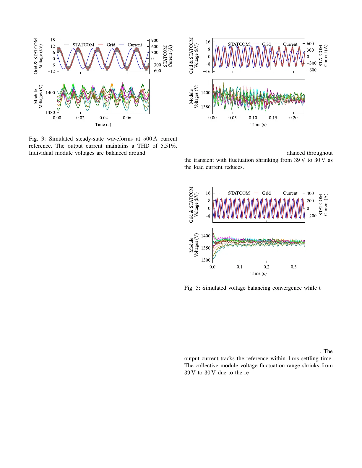
Modular ST A TCOM with Sensor less Module Balancing Based on F our-T ransistor F our-Diode (4T4D) Ser ies / P arallel Chopper Structure Jinshui Zhang, Student Member , Zane Mannings, Chris Dittmer , Angel V P eterche v , Fello w , and Stef an M Goetz, Member Abstract —Static synchr onous compensators (ST A T - COMs) manage reactive power compensation in modern power grids and have become essential for the integra- tion of renewable energy sources such as wind farms. Cascaded H bridges have become the preferred topology for high-power ST A TCOMs, b ut balancing module capaci- tor v oltages remains a persistent challenge . Con ventional solutions equip every module with a voltage sensor—a component that is costly , temperature-sensitive, and prone to aging-related failures. Recent parallel-capable module topologies can balance v oltage thr ough s witched-capacitor operation. The latest developments reduced the sensor requirement fr om one per module to one per arm. Howe ver , these implementations require twice as many individual transistors compared to series-only topologies. W e present a ST A TCOM solution based on the four-transistor four - diode (4T4D) series / parallel chopper cell. This topology achieves bidirectional parallelization with only four transis- tors per module—exactly as many as a conventional full bridge . Fur thermore, we propose a dual-loop contr ol strat- egy that fully eliminates module voltage sensors by infer- ring v oltage levels from the modulation inde x. This sc heme also impro ves output quality by regulating the modulation depth. We validated our proposal through simulation and experiments. W e built a prototype to interface the grid. The prototype further passed rob ustness tests with step change, current direction rever sal, and grid disturbance. This work demonstrates the first modular ST A TCOM im- plementation that combines minim um transistor count with complete elimination of module v oltage sensors. Index T erms —Cascaded con verter , power electronics, reactive power compensation, ST A TCOM, series–parallel cascaded H bridges (CHB), modular multile vel con ver ter , v oltage balancing, hardware-enf orced balancing, switc hed- capacitor operation, direction-selective balancing. I . I N T R O D U C T I O N The concept of the flexible AC transmission system im- prov es the controllability , stability , and power transfer capacity of modern grids [1], [2]. Among these, the static synchronous compensator (ST A TCOM) can dynamically source or sink reactiv e power and distortion to support the grid voltage and correct the po wer factor [3], [4]. Compared with traditional passiv e compensation devices that switch capacitor or inductor banks, ST A TCOMs offer faster response, continuous control, and bidirectional reacti ve power flow . Cascaded bridge circuits (CBCs) / modular multilev el con- verters (MMCs) have become the preferred solution for ST A T - COMs, as they distribute the voltage stress and power load across multiple identical modules [5]. Each module contains a dc capacitor and a set of semiconductor switches that insert or bypass the capacitor v oltage. The number of output voltage lev els scales with the number of modules, which enables high-quality wav eforms without excessi ve filtering. The modular architecture also provides inherent redundancy— faulty modules can be bypassed while the system continues operation. One of the most critical issues in MMCs / CBCs is module voltages drifting apart when indi vidual char ge flo ws are not perfectly balanced over time. This voltage de viation can be influenced by current direction, amplitude, and capacitor as well as semiconductor leakage tolerances. Unequal module voltages entail une ven output steps and wa veform distortion. Sev ere imbalance may cause excessi ve voltage and perma- nently damage the hardware [6]. An extensi ve body of research has focused solely on voltage balancing through control algorithms [7]–[12]. Howe ver , most schemes require ev ery module to be equipped with a voltage sensor—a component that is temperature-sensitiv e, expensiv e, and often fails to guarantee hardware-safe operation indepen- dent of software. Software, ho wev er , is considered a fault- prone element by functional safety standards. One solution circumventing these sensor-related risks is to introduce additional parallel connectivity between modules. Instead of bypassing inacti ve modules, parallel-capable topolo- gies can temporarily connect them to neighboring modules, which establishes direct charge equilibrium [13]–[17]. While paralleled, the module group can act as a single unit with larger effecti ve capacitance, lower source impedance, and reduced voltage ripple. The alternation between series and parallel connectivity between modules and therefore module capacitors is a power - ful operating mode. It enables switched-capacitor behavior in cascaded-bridge con verters. The switched-capacitor behavior is concurrent with the con ventional cascaded-bridge operation. Most importantly , howe ver , the parallel connectivity dras- tically simplifies balancing. It achiev es ideal voltage mainte- nance and charge sharing as a hardware solution [17]–[19]. Balancing can run open loop without error-prone software control or any module voltage sensors. A growing number of topologies hav e been proposed to en- able parallel connectivity in MMCs / CBCs [14]. The cascaded double-H-bridge (CH 2 B) topology offers the most complete functionality with bidirectional parallelization and bipolar out- put capability , but at the cost of eight transistors per module [13]. Symmetrical and asymmetrical double-half-bridge vari- ants halve the switch count but sacrifice output polarity or double the number of capacitors [17], [20]. Diode-clamped and switch-clamped modules provide simplified structures with unidirectional parallelization paths [21]–[26]; howe ver , these topologies cannot guarantee ideal voltage balancing without activ e control assistance. Recent modular ST A TCOM systems exploit those features of a parallel-enabled cascaded topology [27]. This solution reduces the sensor count from one per module to one per arm. Although effecti ve, this approach requires a larger number of individual transistors compared to half or full bridges. The transistor current utilization is as high as in con ventional bridges so that the total amount of silicon is the same, but the many indi vidual transistors also need indi vidual gate dri ving and control. This paper presents a ST A TCOM solution with series and parallel inter-module connectivity b ut only exactly as many transistors as a con ventional H bridge. First members of this class of conv erters were recently presented [28]. These circuits achiev e bidirectional parallelization and bipolar output with only four transistors per module, which is equal to a standard full-bridge without parallel connectivity . In addition, we develop a dual-loop control strategy that completely eliminates module voltage sensors. The inner loop regulates the reactiv e output current, while the outer loop controls the modulation index amplitude and consequently the module voltages. These innov ations together yield an ideally balanced modular ST A TCOM with four transistors, simple balancing, and zero voltage sensors per module. I I . H A R D WA R E D E S I G N A. T opology T able I compares the key characteristics of various mod- ule topologies for cascaded structures. The half-bridge and full-bridge (H bridge) modules represent con ventional de- signs without parallel connection; they rely entirely on activ e software-based balancing control. The CH 2 B topology intro- duced hardware-guaranteed balancing through bidirectional parallelization but requires eight individual transistors and gate dri vers per module, though the same amount of power silicon as H bridges. Symmetrical and asymmetrical double- half-bridge v ariants reduce the number of indi vidual transistors but lose negati ve output polarity or double the capacitor count. Diode- and switch-clamped topologies simplify structures with fewer transistors and a hardware balancing path through parallelization. Ho wev er , this parallelization is purely unidirec- tional and cannot easily implement other features known from cascaded series / parallel con verters. The new 4T4D chopper topology offers all states of other cascaded series / parallel modules, such as the double H bridge, but needs only four transistors. In contrast to diode-clamped cascaded bridges, as another option with a small transistor count, it allo ws full switched-capacitor energy exchange in both directions. Figure 1 illustrates a ST A TCOM with 4T4D cells. Each module comprises one capacitor and two types of chopper half-bridges: T wo diode–switch ( D 1 – T 2 and D 7 – T 8 ) and switch–diode ( T 3 – D 4 and T 5 – D 6 ) choppers require four transistors and four diodes. W e use bipolar power transis- tors, specifically insulated-gate bipolar transistors (IGBTs), which match the diodes well in dynamics and loss behav- ior . T wo adjacent modules are connected through two leads, which transport both the load current (common mode) and the (switched-capacitor) balancing current (differential mode). As in other series / parallel cascaded module structures, the module interconnection can include compact magnetics, also selectiv ely for common- or differential-mode currents to tune parallelization dynamics or distribute output filtering [29]. B. W or king Principles The 4T4D module supports six activ e module- interconnection states (Figure 1). The two Series states provide negati ve and positiv e series connection of the capacitors of adjacent modules. The current flows in parallel through two paths, each with a diode and a transistor for low loss and high semiconductor utilization. The two P arallel states temporarily parallelize the capacitors of the inv olved modules for energy exchange and can enforce the power -flo w direction; the first parallel state only allows power flowing in one direction, the second in the opposite direction. The two Bypass states conduct the load current along either the positiv e or the negati ve rail. A bypassed module does not increase nor reduce the output voltage. In the P assive state, the transistors are off, and the module acts as a rectifier . Like other cascaded bridges, it can still control and contribute to the output voltage but absorbs output power . 1) Direction-Selective P arallelization: The circuit contrasts with other cascaded series / parallel con verters, such as double H-bridge or double half-bridge circuits, in an important detail. In kno wn series / parallel modules, the parallel module state equilibrates paralleled capacitors in either direction. 4T4D cells have two parallel states, which selectiv ely only allo w differential-mode current and power flow in one of the two directions. In the P arallel − mode, capacitor C n − 1 charges C n , whereas the opposite occurs in the P arallel + mode. These two modes offer complementary parallelization directions, which underlies the name dir ection-selective parallel . A control method can exploit the two selectiv e power - flow directions deliberately . If this feature is not needed, the controller can simply alternate between P arallel + and P arallel − for bidirectional energy exchange. A simple rising- edge latch and output status register can alternate the two parallel modes in the modulation scheme. 2) Self-Equalizing Behavior and Reduced P aralleling Loss: The bipolar de vices in 4T4D cells generate a natural equal- ization corridor , which suppresses any oscillations, limits the voltage dif ference between modules to a small band, and reduces loss. Minor v oltage mismatches that fall below this threshold do not trigger a parallelization e vent and therefore produce no paralleling loss. 3) Impedance Matching and T ransistor Design: In the Bypass and P arallel states, 4T4D modules hav e the same equiv alent impedance as con ventional H-bridges—one tran- sistor and one diode in series. In the Series modes, current C n C n-1 D 6 D 7 T 5 T 8 D 4 T 3 D 1 T 2 D 6 D 7 T 5 T 8 D 4 T 3 D 1 T 2 Inter -module connection (n-1) th module n th module T ransistor options + Ener gy storage unit options v statcom i statcom L g R g v g Series – Series + Parallel – Parallel + Bypass – Bypass + D 6 ST A TCOM Circuit Module Structure W orking Principle Fig. 1: A modular ST A TCOM circuit featuring the four-transistor four-diode chopper (4T4D) series / parallel topology . T ABLE I: Comparison of MMC Module T opologies for ST A TCOM Applications Module T opology T ransistor Count Capacitor Count Output Polarity Parallelization Fault Blocking Half-bridge modules (purely series) 2 1 Unipolar None No Full-bridge modules (purely series) 4 1 Bipolar None Y es Double half bridge modules (series / parallel) [17] 4 1 Unipolar Bidirectional No Diode-clamped modules (passiv e parallelization backbone) [21] 2 1 Unipolar Unidirectional No Switch-clamped modules (activ e parallelization backbone) [25] 3 1 Unipolar Unidirectional No Symmetric double half bridge (series / parallel) [20] 4 2 Bipolar Bidirectional No Cascaded double H bridge (series / parallel) [13] 8 1 Bipolar Bidirectional Y es 4T4D series / parallel chopper cell (proposed) 4 1 Bipolar Bidirectional Y es flows through two parallel branches, each with one transistor and one diode. IGBTs provide good impedance matching with the diodes. Furthermore, IGBTs typically offer better o ver- and fault-current capability compared to unipolar field-ef fect transistors. Field-effect transistors may typically outcompete IGBTs in loss at lower voltages, fast switching rates, and lo w currents. Cascaded bridges in medium- and high-voltage applications, such as most ST A TCOMs, typically have to manage grid fault currents, use high module voltages, where the pn forward voltage becomes less relev ant, and operate at low to moderate module switching rates; they still achieve a high effecti ve system-lev el switching rate with low loss [3], [30]. I I I . C O N T R O L A. V oltage Balancing Strategies in Series / Par allel MMC Con ventional modular ST A TCOMs employ a dual-loop con- trol architecture. The inner current loop tracks a sinusoidal reactiv e current reference by adjusting the con verter output voltage. The outer voltage loop measures individual module capacitor voltages, compares them against a common set point, and adjusts the active power exchange with the grid to compensate con verter losses and maintain voltage balance. Series / parallel modular multilev el circuits, such as those based on CH 2 B and also the new 4T4D structure, achie ve local voltage equalization through hardware parallelization. Previous ST A TCOMs with such topologies still require one voltage sensor per arm to form a regulation loop [27]. This sensor measures a representati ve module voltage to detect ov erall drift in the arm’ s energy storage. Despite the reduction of sensors, this approach no w depends critically on a single measurement point per arm. A single sensor f ailure, whether due to temperature drift, aging, or malfunction, can compro- mise the entire arm’ s operation rather than affecting only one module. The inherent reliability concerns of voltage sensors persist. B. Elimination of Module V oltage Sensors through Modu- lation Depth Regulation W e designed a two-stage control that differs from the prior art. The inner loop controls the current. As the module design allows hardware-lev el open-loop balancing of the module ca- pacitor voltages, we could perform additional acti ve balancing, but it is not necessary . W e therefore activ ely control the av erage module voltage in the outer loop to achiev e a certain modulation index A m , i.e., to maximize the output v oltage granularity with a suitable module step size. The feedback signal ˆ A m is extracted from the amplitude of the inner current PI loop’ s output. A dedicated additional sensor is not necessary . The outer loop regulates ˆ A m tow ard a designer-chosen target A ∗ m by adjusting the active po wer exchange with the grid. The module capacitor voltage is not a setpoint; it is an emergent consequence that settles at a value that can satisfy the target modulation depth. This design confers two distinct adv antages over the con- ventional approach. First, sensor elimination follows naturally: ˆ A m is derived from an already-computed signal. Second, the choice of A ∗ m directly governs the con verter’ s steady-state modulation depth, which determines output wav eform quality . A higher A ∗ m driv es the con verter to emplo y more activ e output voltage levels and thereby reduces harmonic distortion. The control of the modulation depth gives the designer an explicit handle on output wa veform quality . This degree of freedom is abs sgn Rising Edge Latch T ruth T able q v o v r ef Carrier #1 Carrier #N q v o Status − 1 +1 − 1 +1 0 × × Series − Series + Parallel − Parallel + Phase-Shifted Carriers PLL v g θ + - COS I r ef + - PI i Amp. Extract PI v + - A m * V i o i r ef ε Â m Fig. 2: Dual-loop control structure for the 4T4D topology based ST A TCOM. The inner current loop controls reactiv e current injection; its PI output dri ves phase-shifted-carrier PWM to synthesize the multilevel output voltage. An additional rising- edge latch alternates the two parallel modes. The outer loop regulates the modulation depth toward a target value A ∗ m , which implicitly sets the module capacitor voltage; its PI output produces a phase offset ε that adjusts the activ e power exchange. absent in con ventional fix ed-voltage-setpoint schemes, where the modulation depth varies passively with grid conditions. The steady-state voltage at the ST A TCOM terminal is modeled by Kirchhoff ’ s voltage law per v o = v g + j ω L g i o + R g i o , (1) where v g , v o , and i o are complex phasors respectiv ely repre- senting the grid voltage, con verter output voltage, and output current; ω is the angular grid frequenc y; and L g and R g are the grid-side inductance and resistance. The con verter synthesizes this voltage from N series- connected submodules per | v o | = A m N X n =1 v sm ,n = A m N V sm , (2) where A m is the modulation index amplitude, V sm is the hardware-equalized module capacitor voltage. The combination of (1) and (2) can regulate the modulation index to A ∗ m , and the module voltage settles to V ∗ sm = | v g + j ω L g i o + R g i o | A ∗ m N ≃ q ( v g + 2 π f g L g i o ) 2 + ( R g i o ) 2 A ∗ m N . (3) This equation shows that setting A ∗ m implicitly determines the av erage steady-state module v oltage V ∗ sm through the pre v ailing grid voltage and output current. C . Modulation-Inde x Estimation Extraction of the current PI controller output amplitude is a core function of the proposed control scheme. W e discuss how to implement it in both single-phase and three-phase settings. 1) Single-Phase ST ATCOM: W e can approximate the cur - rent loop PI output as v m ( t ) = PI i ( i ref − i o ) ≈ ˆ A m sin( ω t + θ o ) . (4) W e use synchronous (I/Q) detection, which exploits the or- thogonality of sinusoidal references, for real-time estimation of the modulation inde x amplitude. The following equations describe a digital implementation. The current PI output can be approximated as v m [ k ] ≈ ˆ A m sin( ω k T s + θ o [ k ]) , (5) where T s is the sampling step. The PI output is multiplied by trigonometric signals syn- chronized to the grid to provide I [ k ] = v m [ k ] cos( ω k T s + θ g [ k ]) , Q [ k ] = v m [ k ] sin( ω k T s + θ g [ k ]) , (6) where θ g is the grid phase angle from the phase-locked loop. Expansion of these products yields dc components plus double-frequency terms as I [ k ] = ˆ A m 2 [sin( θ g − θ o ) + sin(2 ω k T s + θ g + θ o )] , Q [ k ] = ˆ A m 2 [cos( θ g − θ o ) − cos(2 ω k T s + θ g + θ o )] . (7) A first-order recursive low-pass filter extracts the dc compo- nents as ¯ I [ k ] = (1 − α ) ¯ I [ k − 1] + αI [ k ] , ¯ Q [ k ] = (1 − α ) ¯ Q [ k − 1] + αQ [ k ] , (8) where α = 2 π f c /f s sets the filter bandwidth f c . The amplitude is then computed as ˆ A m [ k ] ≈ 2 q ¯ I [ k ] 2 + ¯ Q [ k ] 2 . (9) The filter bandwidth trades off noise rejection against response time. A bandwidth range of f grid / 20 to f grid / 5 can provide adequate smoothing while maintaining an acceptable dynamic response for modulation-index regulation. 2) Three-Phase ST ATCOM: The amplitude estimation con- siderably simplifies in three-phase systems. The Clarke trans- formation naturally decomposes balanced three-phase signals into orthogonal α – β components per v α v β = 2 3 1 − 1 2 − 1 2 0 √ 3 2 − √ 3 2 v a v b v c , (10) where v a , v b , and v c are the three-phase PI controller outputs. The α – β components are inherently orthogonal and equi valent to the I and Q channels deri ved through synchronous detection. The amplitude is then directly obtained as ˆ A m = q v 2 α + v 2 β (11) without explicit quadrature multiplication or lo w-pass filtering. D . Modulation-Index Regulation via Activ e P ow er Control The modulation depth is regulated through controlled acti ve power exchange with the grid. In a ST A TCOM operating ide- ally at unity power factor (pure reactive current), the average activ e power flow is near zero, and module voltages remain constant, neglecting losses. In practice, con verter losses cause a gradual decline in module voltage, which raises the required modulation depth and must be compensated by absorbing a small amount of activ e power from the grid. The active power flow is controlled by adjusting the phase angle ε between the con verter output current and the grid voltage. The outer loop (PI v in Fig. 2) generates this phase offset based on the error between the estimated modulation amplitude ˆ A m and the target A ∗ m . For the same output voltage, a low ˆ A m corresponds to a high module voltage, and vice versa. When ˆ A m > A ∗ m , which indicates that module volt- ages have dropped below their operating point, the controller introduces a small phase lag ( ε < 0 ) that shifts the current wa veform to include an in-phase (activ e) component. This activ e component delivers power to the conv erter , which charges the module capacitors and reduces ˆ A m back to ward A ∗ m . Con versely , when ˆ A m < A ∗ m , a phase lead ( ε > 0 ) causes the con verter to export activ e po wer , which discharges the capacitors and increases ˆ A m . The instantaneous activ e power of the ST A TCOM follows P = V g I o cos( θ g − θ i ) ≈ V g I o sin( ε ) , (12) where V g is the grid voltage amplitude, I o is the output current amplitude, θ g is the grid voltage phase, and θ i = θ g + π / 2 − ε is the current phase for a nominally reactive (leading or lagging by 90 ◦ ) current with phase of fset ε . For small ε , the acti ve power is approximately linear in the phase offset, enabling straightforward PI controller design. The outer modulation-index loop generates this phase offset based on the modulation index error as ε = PI v ( A ∗ m − ˆ A m ) . (13) When module voltages drop, ˆ A m increases to produce a negati ve ε that introduces an in-phase current component to draw activ e power from the grid and recharge the capacitors. In practice, we recommend setting A ∗ m ≈ 0 . 8 . This v alue achiev es a fav orable balance between output wav eform quality and operational headroom. At A ∗ m = 0 . 8 , the con verter employs a large fraction of the av ailable module voltage as productiv e output le vels and yields low harmonic distortion. At the same time, retaining approximately 20% of unused modulation range preserves the conv erter’ s ability to tran- siently increase its output voltage—for example, during a step increase in reactiv e current demand—without immediately saturating the modulation index. A value significantly belo w 0.8 improves headroom b ut degrades output quality , while a v alue near unity may risk modulation saturation under transient conditions. E. Summar y The proposed dual-loop control scheme achieves two objec- tiv es: precise regulation of reactiv e current exchange with the grid, and control of the modulation depth and module voltages. The inner current loop tracks a sinusoidal reference to inject the commanded reactive current, while the outer modulation- index loop adjusts the active power component to compensate for conv erter losses and maintain a healthy modulation depth. The control requires only two measurements: grid voltage (for phase-locked loop synchronization and current reference gen- eration) and output current (for closed-loop current control). No module voltage sensors are needed. I V . D E S I G N C O N S I D E R A T I O N S A N D A P P L I C A T I O N S C O P E A. Operating P oint Constraints The full elimination of module voltage sensors requires careful attention to operating limits during system design. The ST A TCOM output v oltage follo ws from the grid v oltage and the output current as v o = V g + Z L · i o , (14) where Z L is the coupling impedance (primarily inductiv e) and i o is the output current amplitude. For a con verter with N modules, the nominal module voltage equals v o / N . In combination with | v o | = A m N V sm and for purely in- ductiv e coupling ( Z L = j ω L g ), the output current for purely reactiv e operation is i o = A m N V sm − V g ω L g , (15) where V g = | v g | is the grid voltage amplitude. This relation- ship defines the achiev able reacti ve current for a gi ven module voltage and modulation depth. Since the module voltage must remain below the rated limit V sm,max , and the grid voltage may rise to V g,max , the maximum deliv erable current amplitude is bounded per i o ≤ A ∗ m N V sm,max − V g,max ω L g . (16) This constraint must be satisfied at the design stage by choos- ing N and V sm,max appropriately . W e can use this relationship both to select the appropriate number of modules for a given application and to establish a safe operating env elope. B. Application Scope of a Single-Phase ST A TCOM Although the fundamental operating principles of direction- selectiv e parallelization, hardware-guaranteed voltage balanc- ing, and sensorless control apply equally to three-phase imple- mentations, this paper demonstrates the proposed approach us- ing a single-phase ST A TCOM. W e choose this setting for two reasons. First, single-phase operation presents a more demand- ing test case than three-phase systems: without the inherent 12 6 0 6 12 18 Grid & ST A TCOM V oltage (kV) ST A TCOM Grid Current 0.00 0.02 0.04 0.06 T ime (s) 1380 1400 Module V oltages (V) 600 300 0 300 600 900 ST A TCOM Current (A) Fig. 3: Simulated steady-state waveforms at 500 A current reference. The output current maintains a THD of 5.51%. Individual module voltages are balanced around 1396 V with a 30 V fluctuation. balancing provided by symmetrical three-phase currents, all energy storage and voltage regulation burden falls on a single con verter arm. Additionally , the modulation index estimation requires synchronous detection with lo w-pass filtering in the single-phase case, whereas three-phase systems can directly compute the amplitude from Clarke-transformed components without filtering delay . These considerations make the single- phase configuration an effecti ve proving ground for the 4T4D topology and sensorless control strategy . Second, single-phase ST A TCOM applications remain important in sev eral domains. Railway traction systems, particularly those fed by single- phase A C at 25 kV or 15 kV , require reactiv e power com- pensation to mitigate v oltage fluctuations caused by rapidly varying locomotiv e loads [31], [32]. In v arious countries, island microgrids and rural distribution networks often operate with single-phase feeders where localized voltage support is essential for power quality . V . S I M U L A T I O N V A L I D A T I O N W e first de veloped a simulation model in PLECS (v4.9.8, Plexim GmbH) to validate the 4T4D-based ST A TCOM op- eration. This simulation models a 10 kV single-phase system. The shunt-connected ST A TCOM consists of ten modules, each with a nominal voltage range of 1300 V to 1500 V . Each module consists of four IGBTs, four diodes, and a 44 mF capacitor . A. Steady-State Figure 3 sho ws the simulated steady-state wa veforms with the current reference amplitude set at 500 A . The output current achiev es a total harmonic distortion (THD) of 5.51%, and the output voltage THD is 10.66%. The individual module voltages remain well-regulated around 1396 V with a fluctua- tion range of 30 V . 16 8 0 8 16 Grid & ST A TCOM V oltage (kV) ST A TCOM Grid Current 0.00 0.05 0.10 0.15 0.20 T ime (s) 1380 1400 Module V oltages (V) 600 300 0 300 600 ST A TCOM Current (A) Fig. 4: Simulated load step response during a current reference step from 500 A to 250 A . The output current settles within 2 ms . Individual module voltages remain balanced throughout the transient with fluctuation shrinking from 39 V to 30 V as the load current reduces. 8 0 8 16 Grid & ST A TCOM V oltage (kV) ST A TCOM Grid Current 0.0 0.1 0.2 0.3 T ime (s) 1300 1350 1400 Module V oltages (V) 200 0 200 400 ST A TCOM Current (A) Fig. 5: Simulated voltage balancing con ver gence while track- ing a 250 A current reference. Individual module voltages started from an initial spread of ± 5% and con verged to 1374 V within 150 ms. B. Load-Step Response Figure 4 presents the dynamics during a current step. The current reference steps from 500 A to 250 A at 140 ms. The output current tracks the reference within 1 ms settling time. The collectiv e module voltage fluctuation range shrinks from 39 V to 30 V due to the reduction of the load current. C . V oltage Conv ergence Figure 5 presents the dynamics starting with an initial condition in which module voltages span a ± 5% range, i.e., at 1360 V × { 95% , 96% , · · · , 104% } . While the system closely tracks the reference current at 250 A amplitude, the voltage con ver ges to 1374 V within 150 ms without any overshoot. 3-Module ST A TCOM Grid-Connecting Inductor sbRIO-9627 LEM LA 25-P Current Sensor Module Design Fig. 6: Experimental platform for the three-module single- phase 4T4D-based ST A TCOM. The conv erter interfaces an emulated 100 V , 60 Hz grid through a 3 . 58 mH inductor . An embedded controller implements the dual-loop control using only grid v oltage and output current measurements, with no module voltage sensors. T ABLE II: System Specifications Object Parameter V alue Grid-Emulating In verter DC V oltage 100 V Switching Frequency 5 kHz Output Frequency 60 Hz Grid Interface Connection Single-phase Grid Forming Inductance 3 . 58 mH Modular ST A TCOM Number of Modules 3 Nominal Module V oltage 40 V to 50 V Module Capacitance 30 mF Switching Frequency 5 kHz Control Controller sbRIO-9627 T arget Modulation Index 0.8 V I . E X P E R I M E N T A L P L A T F O R M E S T A B L I S H M E N T A. Platform Overview Figure 6 illustrates the platform layout; T able II lists the system specifications. The power grid is emulated with a full-bridge in verter that operates with a dc voltage of 100 V and switching rate of 5 kHz . The three-module ST A TCOM interfaces the emulated single-phase grid through a 3 . 58 mH series inductor . The system injects and absorbs reactiv e current in response to the reference command. The dual-loop control requires only measurements of the grid voltage and the output current; not a single module voltage sensor is used. B. Module Design and P erf or mance Each 4T4D module contains four IGBTs, four silicon diodes, and a 30 mF electrolytic capacitor . Modules are connected with A WG-12 wires without additional discrete inductors or magnetics. 50 100 150 200 Output Power (W) 50 60 70 80 90 100 Ef ficiency (%) 96.9% Error Band Fig. 7: Efficienc y curve on the module level with a 100 V DC link, 20 Ω resistiv e load, and 5 kHz carrier frequency . The peak efficienc y reaches 96.9%. The average stays abov e 93% for output powers abov e 50 W . Fig. 8: Thermal image of a single 4T4D module at steady state with 250 W output. All critical components remain belo w 50 ◦ C . The highest temperature of 48 . 8 ◦ C occurs at an IGBT . W e tested individual module power performance by operat- ing them as inv erters, i.e., we disabled the parallel state and operated A & B as well as C & D in unison . W e measured the efficienc y curv e for the DC-link voltage set to 100 V and a 20 Ω resistiv e load (Fig. 7). The output power is derived from the voltage measured by the oscilloscope probe (THDP0100, T ektronix), and the input power is read from the power supply (HP 6030A) display . The results carry an approximate 5% relativ e uncertainty due to measurement precision. The in verter mode is controlled with a sinusoidal PWM scheme with a carrier frequency of 5 kHz and a dead time of 500 ns . The efficienc y peaks at 96.9% and remains abov e 93% for output power above 50 W . W e monitored the thermal performance at 250 W steady state with a thermal imaging camera (HT -19, Hti). All critical components remain below 50 ◦ C with active air cooling (Fig. 8). The temperature rise of the IGBTs is more significant than that of the diodes. The highest temperature of 48 . 8 ◦ C occurs at the IGBT of Bridge A; all diodes stay below 35 ◦ C . 200 0 200 ST A TCOM V oltage (V) ST A TCOM V oltage ST A TCOM Current 0.00 0.02 0.04 0.06 0.08 t (s) 38 39 40 Module V oltages (V) M1 M2 M3 2.5 0.0 2.5 ST A TCOM Current (A) Fig. 9: Experimental steady-state wav eforms with sev en-lev el output voltage synchronized to the 60 Hz grid. The system regulates the output current to 2 . 5 A with a 90 ◦ phase lag. The three module v oltages stay balanced at 38 . 4 V , 39 . 0 V , and 39 . 7 V . C . Control Platform An sbRIO-9627 embedded controller with field- programmable gate array and signal processing cores (National Instruments) controls the ST A TCOM prototype. The control scheme follo ws Figure 2. Gate signals are generated by the FPGA and distributed to indi vidual module gate driv ers. The grid current is measured through a Hall sensor (LEM, LA 25-P) and then filtered in the embedded controller . The default target modulation index is set to 0.8. The low-pass filter parameter α for modulation index extraction as in (8) is set to 5 × 10 − 5 , which attains an approximate bandwidth of 8 . 3 Hz , for a fast response without inducing voltage overshoots. V I I . E X P E R I M E N T A L R E S U L T S A. Steady State Figure 9 graphs the steady-state wav eforms of the ST A T - COM. The output voltage features a sev en-lev el staircase wa veform synchronized to the 60 Hz grid. The output current is regulated to a 2 . 5 A amplitude with a 90 ◦ phase lag relativ e to the voltage. The modules maintain their voltages at respectiv ely 38 . 4 V , 39 . 0 V , and 39 . 7 V . The v oltage de viation between modules stems from the diode forward voltage in the parallelization paths. B. Load-Step T est Figure 10 represents the system dynamics during a reactive current step from 2 . 5 A to 4 . 0 A . Upon the command change at 8 ms, the current tracks the new reference within a few mil- liseconds. Meanwhile, module voltages instantly drop because of the increased output current and stabilize at a new steady state within the next 200 ms. The new steady-state module 200 0 200 ST A TCOM V oltage (V) ST A TCOM V oltage ST A TCOM Current 0.0 0.1 0.2 0.3 0.4 t (s) 35 40 45 Module V oltages (V) M1 M2 M3 5 0 5 ST A TCOM Current (A) 2.5 A 4 A Fig. 10: System response to a reactive current step from 2 . 5 A to 4 . 0 A . The current tracks the ne w reference within milliseconds. Module voltages experience an instantaneous drop due to the increased current demand, then re-stabilize within 200 ms at a 1 . 4 V higher lev el to maintain the target modulation depth of 0.8. 200 0 200 ST A TCOM V oltage (V) ST A TCOM V oltage ST A TCOM Current 0.0 0.1 0.2 0.3 0.4 t (s) 35 40 45 Module V oltages (V) M1 M2 M3 2.5 0.0 2.5 ST A TCOM Current (A) 2.5 A -2.5 A Fig. 11: System response to a reactiv e current direction rev er- sal at 175 ms, switching from lagging to leading. The current tracks the new reference within a quarter of the output cycle. Module voltages gradually increase to a ne w steady state 2 . 5 V higher on average. voltage increased by 1 . 4 V to maintain a modulation index of 0.8. Figure 11 demonstrates the system dynamics during reacti ve current direction rev ersal. At 175 ms, the ST A TCOM current rev erses direction, i.e., from lagging to leading the grid v olt- age. The current settled to the new reference within a quarter of the output cycle. Meanwhile, module voltages gradually increased to the ne w steady state. The ne w steady-state module voltage increased by 2 . 5 V on av erage. 200 0 200 ST A TCOM V oltage (V) A * m = 0 . 5 A * m = 0 . 8 ST A TCOM V oltage ST A TCOM Current 0.0 0.2 0.4 0.6 0.8 t (s) 40 60 Module V oltages (V) M1 M2 M3 2.5 0.0 2.5 ST A TCOM Current (A) THD (V)=25.3% THD (V)=15.6% Fig. 12: System response to a step change in target modulation depth A ∗ m from 0.5 to 0.8 at 365 ms. At A ∗ m = 0 . 5 , module voltages stabilize at 60 . 1 V with a fiv e-lev el output waveform and current THD of 10.16%. After the step, module voltages settle at 38 V within 200 ms, the output exhibits more levels, and current THD improv es to 7.34%, demonstrating that a higher A ∗ m driv es module v oltages lo wer and yields better output quality . C . V oltage Regulation V alidation Figure 12 demonstrates the modulation-index regulation principle. The trial starts with an A ∗ m value of 0.5; the con- verter produces only fiv e output levels, with module voltages stabilized around 60 . 1 V to deliv er the 2 . 5 A current reference. At time 365 ms, A ∗ m is stepped to 0.8. According to (3), a higher A ∗ m reduces the module voltage. W ithin 200 ms, the system settles at a module v oltage around 38 V , and the output voltage e xhibits additional lev els due to the increased modulation depth. The voltage THD is 25.28% at A ∗ m = 0 . 5 and 15.57% at A ∗ m = 0 . 8 . The current THD is 10.16% at A ∗ m = 0 . 5 and 7.34% at A ∗ m = 0 . 8 . This confirms that a higher A ∗ m yields lower module voltage and better output quality . V I I I . C O N C L U S I O N Previous modular ST A TCOM designs faced a fundamental trade-off: con ventional topologies avoid sensor problems by relying on software-based balancing that demands one volt- age sensor per module, whereas parallel-capable topologies achiev e hardware-guaranteed balancing but require twice the transistors. The latest parallel-capable ST A TCOM research still retains one sensor per arm. This paper breaks that trade-off by combining the 4T4D topology with a fully sensorless dual- loop control strategy . The 4T4D module achieves bidirectional parallelization and bipolar output with only four transistors per module—equal to a con ventional full-bridge—and provides hardware-guaranteed voltage balancing through direct charge equilibration. The proposed outer modulation-index loop elim- inates all module voltage sensors by inferring the module voltage from the amplitude of the current controller output and regulates activ e power exchange to maintain a target modulation depth. The inner current loop provides fast and precise reactive current control. The complete system requires only grid voltage and output current measurements. Simulations and experimental results on a prototype confirm robust operation across steady-state, transient, and grid distur- bance conditions. This work demonstrates the first modular ST A TCOM that simultaneously achieves minimum transistor count and complete elimination of module voltage sensors. R E F E R E N C E S [1] N. G. Hingorani, “Flexible ac transmission, ” IEEE spectrum , vol. 30, no. 4, pp. 40–45, 2002. [2] F . Z. Peng, “Flexible ac transmission systems (facts) and resilient ac distribution systems (racds) in smart grid, ” Proc. IEEE , vol. 105, no. 11, pp. 2099–2115, 2017. [3] B. Singh, R. Saha, A. Chandra, and K. Al-Haddad, “Static synchronous compensators (statcom): a revie w , ” IET power electr onics , vol. 2, no. 4, pp. 297–324, 2009. [4] S. Sharma, S. Gupta, M. Zuhaib, V . Bhuria, H. Malik, A. Almutairi, A. Afthanorhan, and M. A. Hossaini, “ A comprehensive review on statcom: paradigm of modeling, control, stability , optimal location, integration, application, and installation, ” IEEE Access , vol. 12, pp. 2701–2729, 2023. [5] Y . T ang, M. Chen, and L. Ran, “ A compact MMC submodule struc- ture with reduced capacitor size using the stacked switched capacitor architecture, ” IEEE T ransactions on P ower Electronics , vol. 31, DOI 10.1109/TPEL.2015.2511189, no. 10, pp. 6920–6936, 2016. [6] M. M. C. Merlin and T . C. Green, “Cell capacitor sizing in multilev el con verters: cases of the modular multilevel con verter and alternate arm con verter , ” IET P ower Electronics , vol. 8, DOI https://doi.org/10.1049/iet-pel.2014.0328, no. 3, pp. 350–360, 2015. [7] M. W u, Y . W . Li, and G. Konstantinou, “ A comprehensive review of capacitor v oltage balancing strate gies for multile vel converters under selectiv e harmonic elimination pwm, ” IEEE T ransactions on P ower Electr onics , vol. 36, DOI 10.1109/TPEL.2020.3012915, no. 3, pp. 2748– 2767, 2021. [8] F . Ero ˘ glu and A. M. V ural, “ A critical revie w on state-of-charge bal- ancing methods in multilevel converter based battery storage systems, ” Global P ower , Ener gy and Communication Conference (GPECOM) , vol. 4, DOI 10.1109/GPECOM55404.2022.9815810, pp. 14–19, 2022. [9] S. Milovano vi ´ c and D. Duji ´ c, “Comprehensive comparison of modular multilev el converter internal energy balancing methods, ” IEEE T ransac- tions on P ower Electr onics , vol. 36, DOI 10.1109/TPEL.2021.3052607, no. 8, pp. 8962–8977, 2021. [10] G. Konstantinou, H. R. Wickramasinghe, C. D. T ownsend, S. Ceballos, and J. Pou, “Estimation methods and sensor reduction in modular multilev el con verters: A re view , ” International Confer ence on P ower and Ener gy Systems (ICPES) , vol. 8, DOI 10.1109/ICPESYS.2018.8626987, pp. 23–28, 2018. [11] A. Dekka, B. W u, R. L. Fuentes, M. Perez, and N. R. Zar gari, “Evolution of topologies, modeling, control schemes, and applications of modular multilev el conv erters, ” IEEE Journal of Emer ging and Selected T opics in P ower Electronics , vol. 5, DOI 10.1109/JESTPE.2017.2742938, no. 4, pp. 1631–1656, 2017. [12] Z. Ma, T . Hao, F . Gao, N. Li, and X. Gu, “Enhanced SOH balancing method of MMC battery energy storage system with cell equalization capability , ” IEEE Applied P ower Electr onics Conference and Exposition (APEC) , DOI 10.1109/APEC.2018.8341622, pp. 3591–3597, 2018. [13] S. M. Goetz, A. V . Peterchev , and T . W eyh, “Modular multilevel con verter with series and parallel module connectivity: T opology and control, ” IEEE T ransactions on P ower Electr onics , vol. 30, DOI 10.1109/TPEL.2014.2310225, no. 1, pp. 203–215, 2015. [14] J. Fang, F . Blaabjerg, S. Liu, and S. M. Goetz, “ A revie w of multilevel con verters with parallel connectivity , ” IEEE T ransactions on P ower Electr onics , vol. 36, DOI 10.1109/TPEL.2021.3075211, no. 11, pp. 12 468–12 489, 2021. [15] S. M. Goetz, Z. Li, A. V . Peterchev , X. Liang, C. Zhang, and S. M. Lukic, “Sensorless scheduling of the modular multilevel series-parallel con verter: enabling a flexible, efficient, modular battery , ” in 2016 IEEE Applied P ower Electr onics Conference and Exposition (APEC) , DOI 10.1109/APEC.2016.7468193, pp. 2349–2354, 2016. [16] J. Fang, Z. Li, and S. M. Goetz, “Multilevel con verters with symmetrical half-bridge submodules and sensorless voltage balance, ” IEEE Tr ansac- tions on P ower Electr onics , vol. 36, DOI 10.1109/TPEL.2020.3000469, no. 1, pp. 447–458, 2021. [17] Z. Li, R. Lizana F ., S. Sha, Z. Y u, A. V . Peterche v , and S. M. Goetz, “Module implementation and modulation strategy for sensorless balancing in modular multilevel converters, ” IEEE T ransactions on P ower Electronics , vol. 34, DOI 10.1109/TPEL.2018.2886147, no. 9, pp. 8405–8416, 2019. [18] S. M. Goetz, Z. Li, X. Liang, C. Zhang, S. M. Lukic, and A. V . Peterchev , “Control of modular multilevel conv erter with parallel con- nectivity—application to battery systems, ” IEEE Tr ansactions on P ower Electr onics , vol. 32, DOI 10.1109/TPEL.2016.2645884, no. 11, pp. 8381–8392, 2017. [19] J. Zhang, A. V . Peterchev , and S. M. Goetz, “Frequency-dependent impedance variation in multilevel con verters with parallel connectivity , ” in 2024 IEEE Applied P ower Electr onics Conference and Exposition (APEC) , pp. 2337–2341. IEEE, 2024. [20] J. Fang, S. Y ang, H. W ang, N. T ashakor, and S. M. Goetz, “Reduction of MMC capacitances through parallelization of symmetrical half-bridge submodules, ” IEEE T ransactions on P ower Electr onics , vol. 36, DOI 10.1109/TPEL.2021.3049389, no. 8, pp. 8907–8918, 2021. [21] N. T ashakor, M. Kilictas, E. Bagheri, and S. Goetz, “Modular multi- lev el converter with sensorless diode-clamped balancing through level- adjusted phase-shifted modulation, ” IEEE T ransactions on P ower Elec- tr onics , vol. 36, no. 7, pp. 7725–7735, 2020. [22] T . Y in, Y . W ang, X. W ang, S. Y in, S. Sun, and G. Li, “Modular multilev el con verter with capacitor voltage self-balancing using reduced number of voltage sensors, ” in 2018 International P ower Electr onics Conference (IPEC-Niigata 2018-ECCE Asia) , pp. 1455–1459. IEEE, 2018. [23] X. Liu, J. Lv , C. Gao, Z. Chen, and S. Chen, “ A novel statcom based on diode-clamped modular multilevel con verters, ” IEEE T ransactions on P ower Electronics , vol. 32, no. 8, pp. 5964–5977, 2016. [24] T . Zheng, C. Gao, X. Liao, X. Liu, B. Sun, and J. Lv , “ A medium-voltage motor drive based on diode-clamped modular multilevel conv erters, ” in 2017 20th International Conference on Electrical Machines and Systems (ICEMS) , pp. 1–6. IEEE, 2017. [25] N. T ashakor, M. Kılıc ¸ tas ¸ , J. Fang, and S. M. Goetz, “Switch-clamped modular multilevel conv erters with sensorless v oltage balancing con- trol, ” IEEE Tr ansactions on Industrial Electronics , vol. 68, DOI 10.1109/TIE.2020.3028814, no. 10, pp. 9586–9597, 2021. [26] N. T ashakor, D. Keshav arzi, F . Iraji, S. Banana, and S. Goetz, “V oltage estimation in combination with level-adjusted phase-shifted-carrier mod- ulation (LA-PSC) for sensorless balancing of diode-clamped modular multilev el con verters (MMCs), ” IEEE T ransactions on P ower Electron- ics , vol. 38, DOI 10.1109/TPEL.2022.3226421, no. 4, pp. 4267–4278, 2023. [27] Z. Li, J. K. Motwani, Z. Zeng, S. M. Lukic, A. V . Peterchev , and S. M. Goetz, “ A reduced series/parallel module for cascade multilevel static compensators supporting sensorless balancing, ” IEEE Tr ansactions on Industrial Electronics , vol. 68, DOI 10.1109/TIE.2020.2965470, no. 1, pp. 15–24, 2021. [28] J. Zhang and S. M. Goetz, “Direction-selective parallel module structure for cascaded bridge and modular multilevel conv erters with minimum transistor count, ” in IECON 2024-50th Annual Conference of the IEEE Industrial Electr onics Society , pp. 1–6. IEEE, 2024. [29] J. Zhang, B. W ang, X. Tian, A. V . Peterchev , and S. M. Goetz, “ Analytical model and planar magnetic solution for paralleliza- tion surges in switched-capacitor and series/parallel multilev el cir- cuits, ” IEEE T ransactions on Industrial Electr onics , vol. 72, DOI 10.1109/TIE.2024.3472297, no. 5, pp. 4742–4750, 2025. [30] M. Amirrezai, H. Rezaie, and S. M. Goetz, “Feasibility study of incorporating static compensators in distribution networks containing distributed generation considering system power factor , ” Electric P ower Systems Resear ch , vol. 219, DOI https://doi.org/10.1016/j.epsr .2023.109253, p. 109253, 2023. [Online]. A vailable: https://www .sciencedirect.com/science/article/pii/ S0378779623001426 [31] Y . Horita, N. Morishima, M. Kai, M. Onishi, T . Masui, and M. Noguchi, “Single-phase statcom for feeding system of tokaido shinkansen, ” in The 2010 International P ower Electronics Confer ence-ECCE ASIA- , pp. 2165–2170. IEEE, 2010. [32] T . P . Enderle, G. S. da Silva, C. Fischer, R. C. Beltrame, L. Schuch, V . F . Montagner, and C. Rech, “D-statcom applied to single-phase distribution networks: Modeling and control, ” in IECON 2012-38th Annual Conference on IEEE Industrial Electr onics Society , pp. 321– 326. IEEE, 2012.
Original Paper
Loading high-quality paper...
Comments & Academic Discussion
Loading comments...
Leave a Comment