Deep Learning-Driven Black-Box Doherty Power Amplifier with Pixelated Output Combiner and Extended Efficiency Range
This article presents a deep learning-driven inverse design methodology for Doherty power amplifiers (PA) with multi-port pixelated output combiner networks. A deep convolutional neural network (CNN) is developed and trained as an electromagnetic (EM…
Authors: Han Zhou, Haojie Chang, David Widen
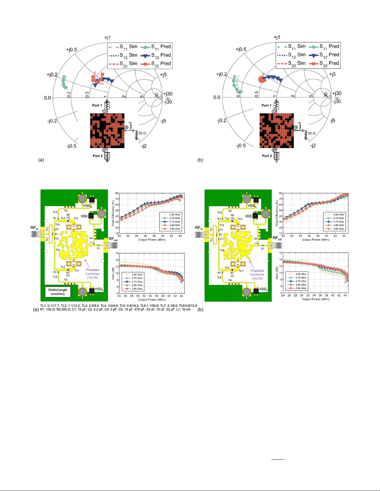
This work has been submitted to the IEEE for possible publication. Copyright may be transferred without notice, after which this version may no longer be accessible. 1 Deep Learning-Dri v en Black-Box Doherty Po wer Amplifier with Pix elated Output Combiner and Extended Ef ficienc y Range Han Zhou, Member , IEEE , Haojie Chang Member , IEEE , and David W id ´ en Abstract —This article presents a deep learning-driv en in verse design methodology for Doherty po wer amplifiers (P A) with multi-port pixelated output combiner networks. A deep con- volutional neural network (CNN) is developed and trained as an electromagnetic (EM) surrogate model to accurately and rapidly predict the S-parameters of pixelated passive networks. By leveraging the CNN-based surrogate model within a black- box Doherty framework and a genetic algorithm (GA)-based optimizer , we effectively synthesize complex Doherty combiners that enable an extended back-off efficiency range using fully symmetrical devices. As a proof of concept, we designed and fabricated two Doherty P A prototypes incorporating three-port pixelated combiners, implemented with GaN HEMT transistors. In measurements, both prototypes demonstrate a maximum drain efficiency exceeding 74% and deliver an output power surpassing 44 . 1 dBm at 2 . 75 GHz . Furthermore, a measured drain efficiency above 52% is maintained at the 9 -dB back-off power level f or both prototypes at the same fr equency . T o evaluate linearity and efficiency under realistic signal conditions, both prototypes are tested using a 20 -MHz 5G new radio (NR)-like wav eform exhibiting a peak-to-average power ratio (P APR) of 9 . 0 -dB. After applying digital predistortion (DPD), each design achieves an average power-added efficiency (P AE) above 51% , while maintaining an adjacent channel leakage ratio (A CLR) better than − 60 . 8 dBc . Index T erms —Deep lear ning, Doherty power amplifier , genetic optimization, in verse design, load modulation, neural networks. I . I N T RO D U C T I O N T O meet the increasing demand for higher data rates, mod- ern communication systems hav e embraced advanced modulation techniques. These methods, howe ver , inherently produce signals with a high peak-to-av erage po wer ratio (P APR). Meanwhile, energy efficiency has become a critical design consideration, as power consumption in mobile net- works constitutes a substantial share of both operational costs and environmental impact. Excessiv e energy usage further complicates system design due to the need for additional cooling infrastructure to manage thermal dissipation. Among all radio front-end components, po wer amplifiers (P A) are typically the most power -intensi ve. Therefore, improving P A efficienc y , particularly under backed-of f output power condi- tions, can yield considerable energy savings and lead to more sustainable and cost-effecti ve network deployments [1]. This research was supported in part by Swedish Innov ation Agency (V innova) Grant 2024-02531, MUL TIRA CS, through the Eureka CEL TIC Framew ork, and in part by VINNO V A, Sivers Semiconductors, and Chalmers Univ ersity of T echnology under Grant 2022-00863. H. Zhou, H. Chang, and D. Wid ´ en are with Chalmers Univ ersity of T echnology , Sweden (e-mail: han.zhou@ieee.org). Activ e load-modulated P A architectures have gained con- siderable attention for their ability to enhance efficiency at back-off power levels. Recent inno vations in this area [2]– [8] have demonstrated notable improvements in back-off effi- ciency . Howe ver , their circuit complexity often hinders prac- tical deployment, especially at higher frequencies. In contrast, the Doherty P A [9] exhibits a simpler circuit configuration, contributing to its widespread commercial adoption. Central to Doherty P A performance is the output combiner network, which go vern the interaction between the main and auxiliary sub-amplifiers. This cooperati ve behavior directly impacts achiev able back-off ef ficiency . In parallel, in verse design methodologies ha ve emerged as a powerful paradigm across diverse fields such as integrated photonics [10]–[12], meta-lens antennas [13]–[15], and scat- tering theory [16], [17]. The core principle is to define a target performance and then determine the optimal structure through a top-do wn approach. This often inv olves pixelating a designated layout area into an N × M binary matrix, where each pixel denotes the presence or absence of a specific material. Compared to con ventional electromagnetic (EM) structures composed of lumped or distributed elements, in verse design enables exploration of a v astly larger design space. In recent years, deep learning has been increasingly applied to such problems for its ability to learn complex features and efficiently navigate high-dimensional design spaces [18]. In radio frequency (RF) circuit design [19], deep learn- ing–based in verse design has been successfully applied to broadband P As, passiv e circuits [20]–[24], and harmonic-tuned Class F P As [25]. Howe ver , most prior work has focused on relativ ely standard structures such as power splitters, filters, and Class B P As with con ventional combiners. Doherty P As, by contrast, require much more sophisticated three-port com- biner networks that integrate load modulation, po wer combin- ing, phase shifting, and impedance transformation within a compact footprint. T o address this gap, we extend the inv erse design methodol- ogy to the synthesis of complex pixelated three-port Doherty combiner networks. In verse design of a traditional Doherty combiner is particularly challenging because it is typically dev eloped through an iterativ e process, resulting in multi- ple cascaded networks such as matching sections, parasitic compensation stages, offset lines, and post-matching circuits in addition to the load modulation network [26]–[29]. This complexity significantly limits the practicality of applying in verse design directly to conv entional combiners. By contrast, 2 Z m Z a I m I a V in V in e - jϴ R ec iproc al & los s y 2 - port c om biner ( Z 2P ) A u x Cla ss C V m + - + - V a M a in Cl a ss B R L Recip roca l & lossle ss 3 - p o rt co m b ine r ( Z 3P ) R L Lu m pe d /d is tri b u te d T/ π n e tw o rk … … Conv ol uti on La y ers F C La y ers Inv er se Desi g n De e p CNN Ba sed EM E m u l a t or Ta rge t Sy nth e s iz e d A u x M a in R L S P aramet ers P ixe lated E M S t r u ctu r e ( N x M ) F o r w ar d Inv er se Desi g n (a) S y m m e tr i c a l m a i n & a u x a m p l i f i e r s w i th e xt e n d e d d y n a m i c r a n g e R a p i d & a cc u r a t e co m b i n e r s y n th e si s u si n g l oad - p u l l d a t a Pr e - d e t e r m i n e d l u m p e d /d i s tr i b u t e d n e twor k co n s tr a i n d e si g n sp a ce L en g th y E M si mu l a ti o n s an d p ar am e t er swe ep s i n cr ease d esi g n ti me (b) Pix e l a t e d l a y ou ts r e p r e sen t e d b y a n N × M b i n a r y m a tr i x, w h e r e e a ch cell (0 or 1) i n d i c a t e s th e a b senc e or p r e senc e of m e t a l Fl e xi b l e a n d r a p i d EM s tr u ct u r e s y n th e si s u si n g d e e p CNN - b a sed su r r og a t e m od e l s a n d g e n e ti c a l g or i th m s (GA ) t o t a r g e t d e si r e d S - p a r a m e t e r s Exp a n d e d d e si g n sp a ce w i th i m p r ov e d so l u ti on s t ow a r d g l ob a l op ti m u m Fig. 1. Overvie w of the proposed deep learning–driv en approach for the synthesis and design of black-box Doherty P As with symmetrical size and extended back-off efficienc y range. (a) Analytical black-box approach for deri ving combiner parameters from load-pull data. (b) Deep learning–based top-down approach employing a pixelated Doherty combiner layout to explore the full design space. adopting the black-box design approach of [30], [31] allows direct synthesis of the complete combiner from transistor load-pull data, eliminating the need to separately design and integrate each sub-netw ork. This methodology greatly smooths the design process and enables extended ef ficiency enhance- ment within fully symmetrical configurations. Nev ertheless, existing black-box approaches are typically limited to com- biner structures composed of lumped or distributed circuit elements, such as transmission lines, capacitors, and inductors. These methods rely on bottom-up design strate gies that in volve parameter sweeps and repeated EM simulations. Although such techniques provide insight into circuit behavior , they inherently constrain the design space to predefined topolo- gies with limited flexibility and a small number of tunable parameters. As a result, existing methodologies restrict the discov ery of higher-performance solutions, require consider- able simulation and optimization time, and ultimately impede the exploitation of the full performance potential of Doherty combiner networks. Motiv ated by these limitations, this work introduces a data-driv en inv erse design framework that relaxes the topological constraints and mitigates the dependence on time-consuming EM simulations and tuning in existing Do- herty combiner synthesis approaches. Building on this foun- dation, we present the first Doherty P A design that combines deep learning–driv en in verse design with a pixelated output combiner network (Fig. 1). A deep con volutional neural net- work (CNN) surrogate model is trained to map pixelated EM structures to their scattering parameters (S-parameters) with high accuracy . Coupled with a genetic algorithm (GA), this surrogate accelerates the inv erse design process by eliminat- ing repeated full-wav e EM simulations. Integrated with the black-box Doherty framework, our method achiev es significant efficienc y improvements at extended back-off lev els using identical transistors directly synthesized from their load-pull data. The remainder of this paper is organized as follows. Section II illustrates the black-box combiner synthesis method- ology and analyzes the Class B/C Doherty P A. Section III details the CNN architecture, data generation workflow , and GA strategy . Section IV demonstrates the implementation process, including two Doherty P A prototypes. Section V reports measurement results. Section VI concludes the paper . I I . T H E B L AC K - B OX C O M B I N E R T H E O RY In this section, the generalized combiner synthesis approach is presented. The parameters of a generic two-port combiner are first deriv ed to analyze the Class B/C Doherty P A behavior with extended efficiency range under v arying dri ve conditions. Then, the synthesis procedure of a two-port Doherty combiner using load-pull data is demonstrated, along with the condition required to transform it into a lossless three-port combiner with resistiv e output loading. A. Blac k-Box Doherty P As Follo wing the analysis in [31], transistors are modeled as ideal, piece wise, voltage-controlled current sources. Only the fundamental component is considered, with higher harmonics short-circuited, representing ideal Class B operation. A phase delay θ is assumed between the output currents of the main and auxiliary amplifiers. The output currents are given by [8] I m = β i m, M (1) I a = 0 , 0 ≤ β ≤ β B β − β B 1 − β B i a,M · e − j θ , β B ≤ β ≤ 1 (2) where β and i denotes the normalized input voltage and fundamental current, respectiv ely . In these expressions, the 3 C a s e I C a s e I I C a s e I I I Back - Off V in ( β B ) 0 .5 0 .3 8 0 .23 Cu rren t R atio ( a ) 1 .0 0. 9 0 .8 Ba ck - Off P o ut ( γ ) 6 d B 7 d B 9 d B (a) ( b ) ( c ) Fig. 2. Illustration of the black-box technique under different dri ving conditions. The output po wer is normalized to the corresponding saturated output power for each current-scaling ratio. (a) Normalized current driv e profiles as a function of input voltage. (b) Theoretical performance comparison for different drive profiles (Cases I–III). (c) Corresponding current ratios and back-off levels for each case. first subscript (m or a) refers to the main or auxiliary amplifier , respectiv ely , and the second subscript (M or B) denotes operation at maximum or back-off power levels. The combiner network is described by its impedance matrix Z 2P , relating voltages and currents at the amplifier outputs V m V a = Z 2P I m I a = Z 11 Z 12 Z 12 Z 22 I m I a (3) Assuming an optimal load of R opt for the main amplifier , the auxiliary amplifier’ s optimal load reduces to R opt /α , with α defined as the ratio of peak output currents between the main and auxiliary amplifiers. The combiner’ s impedance parameters are then derived as [32] Z 11 = R opt β B Z 12 = 1 − 1 β B R opt α e j θ Z 22 = 1 β B + α e − j 2 θ − 1 R opt α 2 e j 2 θ (4) T o transform the lossy reciprocal two-port network into an equiv alent lossless three-port combiner with resistive termina- tion, the following condition must be satisfied [30] ℜ{ Z 12 } 2 = ℜ{ Z 11 }ℜ{ Z 22 } (5) The normalized output power back-of f lev el, denoted by γ , and the phase delay θ are derived as [32] γ = 1 + α β B (6) θ = kπ ± arcsin s β B ( α − β B + 1) 1 − β 2 B (7) where k is an arbitrary integer . Expressions (4–7) indicate that, for a giv en back-off level γ and current ratio α , a valid phase shift θ and correspond- ing combiner impedance matrix Z 2P can be determined. As illustrated in Fig. 2, the theoretical analysis suggests that this method enables the realization of desired back-off le vels across various current ratios, facilitating full utilization of the main and auxiliary transistors. B. Combiner Synthesized from Load-Pull Data The theoretical analysis abov e demonstrates the fundamen- tal operating principle of the black-box approach. Ho wev er , at high frequencies, transistor parasitics and nonlinearities significantly influence P A performance. As a result, a combiner design methodology guided by nonlinear device behavior un- der large-signal excitation becomes essential for fully utilizing the device capabilities. The two-port combiner impedance matrix ( Z 2P ) can be derived from load-pull data, as follo ws. Z 11 = ( Z a , M + Z a , off ) Z m , B α 2 + ( Z m , M − Z m , B ) Z m , M Z m , M − Z m , B + ( Z a , M + Z a , off ) α 2 Z 12 = ( Z m , M − Z m , B ) ( Z a , M + Z a , off ) α Z m , M − Z m , B + ( Z a , M + Z a , off ) α 2 Z 22 = ( Z a , M + Z a , off ) Z a , M α 2 + ( Z m , B − Z m , M ) Z a , off Z m , M − Z m , B + ( Z a , M + Z a , off ) α 2 (8) The parameter α is gi ven by α = i a,M i m,M = s ℜ{ Z m,M } P a,M ℜ{ Z a,M } P m,M e − j θ (9) where P represents the deli vered output po wer and Z is the optimal impedance, both from load-pull data. Furthermore, when selecting the design parameter for the back-off power lev el ( γ B ), the following relationship must be satisfied to ensure power conserv ation γ B P m,B = P m,M + P a,M (10) T o implement a physically realizable, lossless three-port combiner ( Z 3P ) terminated with a resistiv e load R L , the synthesized lossy two-port network ( Z 2P ) must satisfy the condition described in equation (5). Giv en equations (5), (8), and (9), the only remaining unknown is the phase parameter 4 S Param e te rs P ix e lat e d E M S t r u c t u r e ( N x M ) Fea t u r e M a p s FC L a y e r s C o n v o lut ion a l L a y e r B a t c h N o r m . R e L U Fig. 3. Architecture of the trained deep CNN with residual connections. The input is a binary 15 × 15 matrix representing the pixelated EM layout structure, and the output is the predicted real and imaginary components of the corresponding S-parameters across the frequency range of interest. P ix e lat e d L a y o u t ( N x M ) R L M a in A u x ① 1 ② ③ ④ V D D Fig. 4. The employed pixelated Doherty combiner networks, where the feed locations for the main (port 1 ), auxiliary (port 2 ), and output (port 3 ) are placed at the center of each corresponding edge of the 15 -pixel array . The output port 3 is connected to the load ( R L ), while port 4 is left open. θ , which can be solved analytically or numerically . Once θ is determined, the complete impedance matrix Z 2P for the combiner can be fully specified. I I I . D E E P L E A R N I N G - D R I V E N I N V E R S E S Y N T H E S I S O F D O H E RT Y C O M B I N E R N E T W O R K Building upon the theoretical analysis and equations in Section II, a two-port Doherty combiner matrix Z 2P can be directly derived from load-pull data, enabling designs with extended back-of f efficiency while fully utilizing the emplo yed transistors. Ho we ver , physical realizations of such combiners hav e traditionally relied on predefined lumped or distributed topologies, often depending on expert intuition, iterati ve EM simulations, and manual parameter tuning [30], [31]. T o overcome these limitations, this section introduces an in- verse design methodology for synthesizing Doherty combiners using pixelated output networks. This approach enables explo- ration of a broader design space encompassing all fabricable structures. W e begin by describing the pix elated layout design space and the corresponding training dataset. This is followed by the development of a deep CNN used as an EM surrogate T ABLE I D E T A I L E D C O N FI GU R A T I ON O F T HE D E E P CN N A R CH I T E CT U R E Con v . Layer Filter Size Filter Number Inputs C 1 12 × 12 32 Matrix in C 2 12 × 12 32 C 1 C 3 10 × 10 32 C 2 + Matrix in C 4 10 × 10 32 C 3 C 5 8 × 8 32 C 4 + C 2 C 6 8 × 8 32 C 5 C 7 6 × 6 32 C 6 + C 4 C 8 6 × 6 32 C 7 C 9 4 × 4 32 C 8 + C 6 C 10 4 × 4 32 C 9 C 11 3 × 3 32 C 10 + C 8 C 12 3 × 3 32 C 11 FC Layer Num. Neur ons Dropout Act. Func. F 1 2048 0.25 LeReLU (0.01) F 2 2048 0.25 LeReLU (0.01) F 3 2048 0.25 LeReLU (0.01) F 4 2048 0.25 LeReLU (0.01) F 5 2048 0.25 LeReLU (0.01) F 6 78 0 T anh model, as shown in Fig. 3. Lastly , the in verse synthesis process is detailed using a GA optimizer . A. Pixelated Doherty Combiner Network T o synthesize compact and lo w-loss Doherty combiner networks, a planar circuit layout is defined over a ground plane and discretized into a two-dimensional binary pixel grid. Each pix el is assigned a binary value: “1” represents the presence of metal, and “0” denotes a dielectric (non- metal) region. The layout is partitioned into a 15 × 15 grid, where each pixel measures 1 . 8 × 1 . 8 mm . This resolution is selected to balance EM coupling fidelity and the feasibility of model training [25]. A higher pixel resolution enables finer structural detail and access to a larger design space, potentially yielding improved performance at the expense of increased computational requirements. T o ensure reliable 5 electrical connecti vity , particularly across diagonal paths, a 20% metal ov erlap is applied to each metal pixel. This results in a total physical combiner size of 27 . 36 mm × 27 . 36 mm . As illustrated in Fig. 4, the feed locations for the main (port 1 ) and auxiliary (port 2 ) amplifiers, as well as the output (port 3 ) connected to the load resistance ( R L ), are placed at the center of each corresponding edge of the 15-pixel array . T o enable DC biasing of the transistors, supply feeds (VDD) are introduced ahead of R L , allowing the implementation of RF chokes and DC blocks. The binary representation of this pixelated layout results in a total design space of 2 225 possible EM structures. Given the vastness of this space, brute-force exploration is compu- tationally infeasible in both time and memory . This challenge presents a compelling opportunity for deep learning. If a deep neural network can be trained as a surrogate EM model using a much smaller subset of simulation data ( < 100000 ), it can then accurately and rapidly predict the scattering parameters of arbitrary pix elated layouts. This surrogate model ef fectively re- places time-intensive EM simulations gov erned by Maxwell’ s equations. When combined with a GA optimizer and guided by a target specification, the in verse design of pixelated structures can be effecti vely achiev ed. B. Deep Convolutional Neural Network The pixelated circuit layout can be naturally interpreted as a structured image, making CNNs, widely used in computer vision and image processing, well suited for this task. CNNs effecti vely model local spatial interactions and capture EM coupling between adjacent pixels by learning hierarchical fea- tures. In the follo wing texts, we present the dataset generation process used for CNN training and describe the architecture of the proposed deep CNN model. 1) Data Generation and Augumentation: A dataset com- prising div erse binary matrices representing pixelated EM structures and their corresponding S-parameters is essential for training the CNN. W e fully automated the data generation process using Python scripts, which create pixelated layouts in K eysight Adv anced Design System (ADS) and execute EM simulations using Momentum in ADS. The training circuits are generated by assigning each layout a random percentage of metal pixels, drawn from a normal distribution centered at 50% with a standard deviation of 15% . During data generation, we ensure that each circuit maintains connectivity between the ports by applying a depth-first search (DFS) algorithm to verify continuous electrical paths. W e simulate a total of 77000 four-port pixelated EM structures, running four simulations in parallel. Each circuit simulation takes around 24 seconds. Using an Intel i5-14600KF CPU, the total time required to generate the dataset is approximately 129 hours. Each simulated structure includes four ports, with one port terminated in an open condition and another port terminated with a 50 Ω load during augmentation. By applying rotations, translations, and mirror reflections [20], we generate additional three-port EM structures with a 50 Ω load termination, where the S-parameters are derived directly from the original four - port simulations. W e augment the data such that for every Algorithm 1 Genetic Algorithm Optimization Require: Desired S-parameter profile; trained CNN surrogate model; population size N ; maximum iterations X etc. Ensure: Optimal pixelated layouts with target S-parameters. 1: Select a target S-parameter profile. 2: Generate N binary matrices with direct connections, sam- pled from a normal metal pix el density distribution. 3: f or each generation up to X iterations do 4: Predict S-parameters of all candidate circuits using the trained deep CNN model. 5: Calculate fitness based on deviation from the target S- parameter profile. 6: if fitness of best candidate meets target then 7: break loop; optimal solution found. 8: end if 9: Retain the top 10 circuits as elite indi viduals for the next generation. 10: Add up to 30% new random circuits depending on current iteration count to maintain di versity . 11: Perform tournament selection: • Split and recombine rows for crossover . • Flip 1 − 10% of pixels randomly for mutation. • Fill population up to N circuits. 12: end for 13: r eturn The best pixelated circuit layout achieving or approaching the target S-parameter profile. simulated circuit, eight training data points are created, sig- nificantly reducing the effecti ve dataset creation time. After augmentation, the total dataset size is approximately 1 . 5 GB . 2) Deep CNN Ar chitectur e: As illustrated in Fig. 3, the deep CNN architecture consists of twelve conv olutional layers and six fully connected (FC) layers. A residual network (ResNet) structure is employed to mitigate the vanishing gradient problem, which improves training stability and accel- erates con vergence [33]. Leaky rectified linear unit (LeReLU) functions are applied as activ ation functions after batch nor- malization [34], enabling the network to learn complex non- linear relationships. In the con volutional layers, local spatial features are effecti vely extracted from the binary input matrix representing the pixelated EM layout. These feature maps are then flattened into a one-dimensional v ector, which is passed to the FC layers for further processing. During training, dropout layers are inserted to reduce the risk of overfitting [35]. Each con volutional layer uses 32 filters, and each FC layer contains 2048 neurons with a dropout rate of 25% . The CNN takes binary matrices as input and produces real and imaginary components of the S-parameters as output. A detailed ov ervie w of the network architecture is provided in T able I. W e train the network using the mean absolute error (MAE) loss function, which quantifies the a verage absolute dif ference between predicted and actual values, and is defined by L = 1 N N X i =1 | y i − ˆ y i | (11) where y i and ˆ y i denote the actual and predicted values, 6 T ABLE II L OA D - PU L L D A TA O B TAI N E D A T 2 . 75 GHz Main Amplifier Auxilary Amplifier Z opt ( Ω ) P del (dBm) P AE ( % ) Z opt ( Ω ) P del (dBm) P AE ( % ) Peak Power Level 14 . 3 + j 1 . 6 42 . 7 74 14 . 3 + j 1 . 6 42 . 1 78 Back-Off Power Lev el 7 . 2 + j 15 . 3 36 . 4 57 0 . 25 + j 21 . 1 (Off) - - respectiv ely . The Adam optimizer [36] is used with an initial learning rate of 0 . 001 , which we reduce by a factor of 0 . 93 ev ery 10 epochs to aid con vergence. The neural network is trained for 300 epochs using a batch size of 2790 . Upon completion, the model achiev es a mean absolute error (MAE) of 0 . 068 , demonstrating high prediction accurac y . C. Genetic Algorithm-Based Inver se Synthesis The in verse synthesis of pixelated Doherty combiners is performed using a GA to efficiently explore the vast design space. As illustrated in Algorithm 1, the process begins by defining a desired S-parameter profile, which serv es as the target specification. W e then generate an initial population of N = 4000 binary matrices representing connected circuit lay- outs, sampling metal pixel densities from a normal distribution to ensure a diverse starting point. The trained CNN surrogate model is used to rapidly predict the S-parameters of all candidate circuits in each generation, and fitness scores are calculated based on the deviation from the target S-parameter profile. If the fitness of the best can- didate circuit meets the tar get performance or after X = 240 iterations, the algorithm is terminated. Otherwise, the top 10 circuits with the highest fitness scores are retained as elite individuals for the next generation. T o maintain div ersity , up to 30% of the population is replaced with new random circuits depending on the current iteration count. This encourages exploration during the early stages of the optimization while focusing on refinement in later generations. T ournament selection is performed to identify parent pairs for crossover , where rows of parent matrices are split at random points and recombined to produce offspring. W e also apply a mutation step by flipping between 1% and 10% of the pixels in the offspring circuits, introducing additional variability and helping to a void con vergence to local minima. This iterative process continues until the termination criterion is satisfied, gradually refining the population to ward circuits that match the desired S-parameter response. I V . D E E P L E A R N I N G - D R I V E N D O H E R TY P A D E S I G N In this section, we present the design of two prototype Doherty P As using the proposed black-box synthesis method- ology augmented by deep learning. The objectiv e is to demon- strate the complete design procedure and validate the ef fecti ve- ness of the proposed approach. T o ensure a fair and focused ev aluation, the input networks of both Doherty P As are kept completely identical. The only difference lies in the output Doherty combiners, which are in- dividually synthesized using the proposed deep learning-aided in verse design strate gy . This setup highlights the div ersity of synthesis solutions achiev able with the method, as well as its robustness and flexibility . For both the main and auxiliary branches, we employ the same commercially available 10-W GaN HEMT transistor form (CG2H40010F , MACOM) as the activ e device. This choice ensures symmetry in the de vice characteristics. A. Blac k-Box Doherty P A Design Based on Load-Pull Data W e begin by designing both amplifier branches using the MA COM transistors (CG2H40010F). The input network, including matching, stabilization, and biasing circuits, is identically designed and fixed for both Doherty prototypes. Low-impedance open stubs connected to the transistor gates, together with series RC networks at the inputs, are employed to simultaneously ensure unconditional stability and match the optimal source impedances of the transistors. In addition, resistors are incorporated in the gate bias lines to further enhance stability . A W ilkinson power divider is then used to equally distribute the input signal to the main and auxiliary amplifier branches. Next, we select the desired back-off power lev el ( γ B = 9 dB ) and configure the gate bias of the main amplifier . Note that main amplifier’ s gate bias in volves a trade- off between gain and efficiency: biasing the main amplifier closer to Class AB operation improves gain performance but can reduce efficienc y . In our design, we set the main amplifier’ s gate bias to achie ve a quiescent current of 40 mA . For the auxiliary amplifier , we set the gate bias in Class C op- eration. Selecting the auxiliary gate bias may require iterati ve adjustments to ensure that the auxiliary amplifier acti v ates at the desired 9 dB back-off lev el. Load-pull characterization of the main and auxiliary ampli- fiers is performed at both the peak output and the specified back-off power le vel. These simulations are conducted using the bias conditions established in the preceding design phase. It should be noted that when selecting the optimal load impedance, multiple degrees of freedom exist to trade off efficienc y , output power , and linearity . In this work, we pri- oritize maximizing efficiency at the back-off power lev el and maximizing delivered output power at the peak power level. The extracted optimal impedances and corresponding power performance for both Doherty prototypes at peak and back- off conditions are summarized in T able II. Using equations (8)–(10), together with equation (5), we deriv e the phase parameter solution of θ = 133 . 4 ◦ and the corresponding two- port combiner impedance matrix ( Z 2P ) as Z 2P = 1.35 + j 6.94 − 5.37 + j 14.02 − 5.37 + j 14.02 21.27 + j 16.10 (12) The obtained Z 2P matrix fully specifies the desired Doherty combiner behavior in a reciprocal two-port black-box form, 7 (a) (b) 1 ③ Port 1 Port 2 50 Ω 1 ③ Port 1 Port 2 50 Ω ① ② ① ② Fig. 5. The two synthesized pixelated Doherty combiner netw orks, (a) and (b), along with their EM-simulated S-parameter results compared to the corresponding responses predicted by the deep learning approach, ov er the frequency range of 2 . 55 – 2 . 95 GHz . RF in W idt h / L e n g t h ( m m/ mm ) RF in (a) ( b ) R1 C1 C1 T L 2 T L 3 T L4 T L 6 T L 3 T L 5 T L 7 T L 8 R1 R1 R2 C 2 R1 C3 Cb Cb Cb C1 L1 R1 C1 C1 TL 2 T L 3 T L4 T L 6 T L 3 T L 5 T L 7 T L 8 R1 R1 R2 C 2 R1 C3 Cb Cb Cb C1 L1 P ix e lat e d C o m b ine r ( 1 5 x 1 5 ) Pi x e la t e d C o m b ine r ( 1 5 x 1 5 ) TL1 : 0 . 1 / 1 7 . 7 ; TL2 : 1 . 1 / 1 2 . 0 ; TL3 : 2 . 0 / 9 . 0 ; TL4 : 3 . 0 / 4 . 6 ; TL5 : 0 . 8 / 1 4 . 2 ; TL6 : 1 . 1 / 3 0 . 8 ; TL7 : 2 . 1 / 8 . 5 ; TL8 : 0 . 8 / 1 2 . 9 R 1 : 1 0 0 Ω; R 2 : 2 0 0 Ω; C 1 : 1 5 p F; C 2 : 2 . 2 p F; C 3 : 3 p F: Cb : 1 5 p F, 4 7 0 p F, 3 3 nF , 1 0 uF , 2 2 uF ; L 1 : 1 0 nH RF out RF out V GG m V D D V GG a V GG m V D D V GG a Fig. 6. Full circuit schematic of the proposed deep learning-dri ven pixelated Doherty P As: a) prototype 1 and (b) prototype 2. The corresponding full EM simulation results show the lar ge-signal performance in terms of drain efficienc y and gain versus output po wer over the frequenc y range of 2 . 65 − 2 . 85 GHz . specifying the impedance relationships required for achieving proper load modulation and matching. By implementing this impedance matrix as a lossless three-port combiner with all lossy resisti ve components consolidated into a single port, the Doherty P A can achieve the correct load trajectories across the entire back-off range, enabling an efficiency enhancement at γ B = 9 dB . Successfully implementing this combiner network represents a critical step, as the associated design space is vast and requires systematic exploration. B. Pixelated Doherty Combiner Synthesis Giv en the desired two-port impedance matrix derived ear - lier , we first con vert this matrix into its corresponding scatter- ing matrix, which specifies the target S-parameter behavior of the combiner network. T o realize a physical implementation matching this target response, we use the GA in combina- tion with the trained deep CNN surrogate model to search the vast pixelated design space efficiently . Unlike traditional approaches that require time-intensiv e EM simulations for ev ery candidate structure, our deep learning-based method allows the CNN surrogate model to rapidly predict the S- parameters of thousands of pixelated layouts within a second per optimization step. This dramatically accelerates the design process compared to conv entional brute-force EM sweeps. During the optimization, we ev aluate each candidate’ s pre- dicted S-parameters by calculating a fitness v alue based on how closely the y match the target scattering parameters. The fitness function is defined as F = 1 e + ϵ (13) 8 (a) (b) LM T raj ec t ory * P B O - > P P e a k P B O - > P P e a k Fig. 7. (a) Power-deli vered contours (maximum and -0.3 dB) and efficiency contours (maximum and -3% of the main amplifier for prototype 1 at peak and back-of f output po wer, together with its load-modulation (LM) trajectory . (b) Load-modulation trajectories of the main and auxiliary amplifiers at the current-generator plane at the design center frequency . where the error term e is defined as e = max X ℜ{ ˆ S i } − ℜ{ ¯ S i } , X ℑ{ ˆ S i } − ℑ{ ¯ S i } (14) with ˆ S i − ¯ S i representing the absolute errors between the predicted and target values for both the real and imaginary parts of S 11 , S 12 , and S 22 . A small constant ϵ = 10 − 5 is included in the denominator to ensure numerical stability during fitness calculation. Based on this optimization strategy , we synthesize two pixelated Doherty combiner networks, as shown in Fig. 5. The two solutions illustrate the stochastic nature of the GA, rev ealing that multiple distinct pixelated combiner networks can satisfy the same S-parameter targets for Doherty oper - ation. Note that all three ports are terminated with 50 Ω during the simulations. The agreement observed between the EM-simulated S-parameters and the predictions generated by the CNN surrogate model demonstrates reasonable accurac y of the proposed deep learning–assisted design methodology . It is acknowledged that the prediction accuracy is subject to lim- itations, particularly when modeling S-parameters with small magnitudes. This agreement could be further improv ed by expanding the training dataset, enhancing the neural network architecture, and increasing the number of training epochs, giv en suf ficient computational resources. Overall, these results confirm that the proposed approach effecti vely captures the complex EM interactions within the pixelated structures and enables efficient exploration of a large design space. C. Simulation Results Fig. 6 demonstrated the complete circuit schematics of the two fabricated Doherty P A prototypes. EM simulations of (a) ( b ) RF in RF out RF in RF out V G G m V G G a V DD V G G a VG G m V DD P i x el ate d Com bi ne r ( 15 x 15 ) P i x el ate d Com bi ne r ( 15 x 15 ) Fig. 8. Photograph of the fabricated deep learning-driven Doherty P As with pixelated output combiners: (a) prototype 1 and (b) prototype 2. all transmission lines are performed using Momentum within Ke ysight ADS. W e use accurate models from Modelithics for all lumped components, and transistor models provided by Macom are employed to ensure reliable simulation results. The simulated ef ficiency and gain of the two prototypes versus output po wer at different operating frequencies are pre- sented in Fig. 6. Excellent ef ficiency is observed across both saturation and back-off operating points within the targeted frequency band. At the center frequency of 2 . 75 GHz , both prototypes achie ve a peak drain efficienc y e xceeding 78% , deliv ering more than 44 . 2 dBm saturated output power . More- ov er , drain ef ficiency remains abov e 60% at the designated 9 -dB back-off point. T o further illustrate the large-signal behavior , Fig. 7(a) presents the deli vered-power contours, drain-efficienc y con- tours, and load-modulation trajectory of the main amplifier for prototype 1 as a representativ e example at both peak and back-off operating points. The deliv ered-power contours indicate the maximum output power and the output-power contour within 0 . 3 -dB of this maximum, while the efficienc y contours denote the maximum achieved drain efficienc y and the corresponding 3% degradation boundary . In addition, the intrinsic load-modulation trajectory is shown in Fig. 7(b), clearly rev ealing the characteristic load-modulation behav- ior of a Doherty P A. Overall, both prototypes demonstrate consistent large-signal performance across the entire design bandwidth, thereby validating the robustness and practical viability of the proposed synthesis approach. V . M E A S U R E M E N T R E S U L T S A photograph of the two fabricated Doherty P A prototypes is shown in Fig. 8. The prototype circuits are fabricated on a 20-mil-thick Rogers 4350B substrate, each with a compact size of 60 × 110 mm 2 . The manufactured printed circuit boards (PCBs) and the employed CG2H40010F GaN HEMT transistors are mounted on brass fixtures, which also serve as heat sinks for thermal management. W e perform small-signal, continuous-wa ve (CW), and modulated-signal measurements 9 Fig. 9. Measurement setup: (a) small-signal and CW measurements, and (b) modulated-signal measurements. 2.3 2.5 2.7 2.9 3.1 3.3 Frequency (GHz) -40 -30 -20 -10 0 10 20 Scattering Parameters (dB) (a) S 11 sim S 11 mea S 21 sim S 21 mea S 22 sim S 22 mea 2.3 2.5 2.7 2.9 3.1 3.3 Frequency (GHz) -40 -30 -20 -10 0 10 20 Scattering Parameters (dB) (b) S 11 sim S 11 mea S 21 sim S 21 mea S 22 sim S 22 mea Fig. 10. Measured and simulated S-parameters of the fabricated Doherty P As: (a) prototype 1 and (b) prototype 2. to thoroughly characterize the fabricated Doherty prototypes. T o ensure consistency , the drain supply voltage is set to 28 V for both prototypes throughout all measurements. Specifically , a quiescent current of 40 mA is set to the main amplifiers, while the gate bias of the auxiliary amplifiers is fixed at − 7 V . The measurement setup is shown in Fig. 9. Small-signal measurements are performed using a Ke ysight PN A-X network analyzer . For CW measurements, a signal generator provides the CW excitation, and the output power is measured using a power meter . T o improve measurement accuracy , a low-pass filter is inserted at the output to suppress harmonic components and pre vent them from entering the power meter . Moreover , a broadband linear driv er amplifier supplies sufficient input power to drive the prototype circuits. F or modulated-signal measurements, a K eysight PXIe vector transceiver (VXT M9421) generates and captures the modulated signals. A. Small Signal The performance of the two Doherty prototypes was first assessed through small-signal measurements to determine their frequency responses. As shown in Fig. 10, the strong corre- lation between simulated and measured data confirms proper operation. W ithin the 2 . 5–3 . 1 GHz range, both designs achie ve a measured small-signal gain ( S 21 ) exceeding 10 dB, while maintaining an input return loss ( S 11 ) better than -8 dB across the entire band. B. Continuous W ave Fig. 11 presents the measured drain ef ficiency and gain as functions of output power for frequencies spanning 2 . 65 to 2 . 85GHz in 50 -MHz steps. At the center design frequency of 2 . 75 GHz , Doherty prototype 1 achieves a measured peak drain efficiency of 74% with a maximum output power of 44 . 1 dBm , and a measured drain ef ficiency of 55% at 9 - dB back-off po wer lev el. Meanwhile, Doherty prototype 2 reaches a peak drain efficiency of 76% with a peak output power of 44 . 8 dBm , and achie ves a measured drain efficienc y of 51% at the 9 -dB back-off level. The performance of both prototypes versus frequency is also shown in Fig. 11, where the drain efficienc y and po wer-added ef ficiency (P AE) at both the peak output power level and the 9 -dB back-off lev el are presented, along with the peak output power . Across the frequency range from 2 . 65 to 2 . 85 GHz , the measured peak and 9 -dB back-off ef ficiency for both prototypes exceed 68% and 46% , respectiv ely . These results clearly demonstrate that excellent high- efficienc y enhancement is achiev ed around the 9 -dB back- off power lev el, accompanied by a power gain compression 10 30 32 34 36 38 40 42 44 Output Power (dBm) 10 20 30 40 50 60 70 80 Drain Efficiency (%) 2.65 GHz 2.70 GHz 2.75 GHz 2.80 GHz 2.85 GHz (a) 24 26 28 30 32 34 36 38 40 42 44 Output Power (dBm) 4 6 8 10 12 14 16 Gain (dB) 2.65 GHz 2.70 GHz 2.75 GHz 2.80 GHz 2.85 GHz (b) Frequency(GHz) 2.55 2.65 2.75 2.85 2.95 Power(dBm)&Efficiency(%) 10 20 30 40 50 60 70 80 DE Max DE BO P AE Max P AE BO P Max (c) 30 32 34 36 38 40 42 44 Output Power (dBm) 10 20 30 40 50 60 70 80 Drain Efficiency (%) 2.65 GHz 2.70 GHz 2.75 GHz 2.80 GHz 2.85 GHz (d) 24 26 28 30 32 34 36 38 40 42 44 Output Power (dBm) 4 6 8 10 12 14 16 Gain (dB) 2.65 GHz 2.70 GHz 2.75 GHz 2.80 GHz 2.85 GHz (e) Frequency(GHz) 2.55 2.65 2.75 2.85 2.95 Power(dBm)&Efficiency(%) 10 20 30 40 50 60 70 80 DE Max DE BO P AE Max P AE BO P Max (f) Fig. 11. Measured drain ef ficiency and gain of the Doherty prototype circuits versus output power , along with measured peak and back-off drain efficiency , P AE, and output power versus frequency: (a–c) prototype 1 and (d–f) prototype 2. Fig. 12. Measured output spectrum, AM–AM/AM–PM characteristics, and constellation diagram under a 20-MHz, 9-dB P APR 5G NR-like communication signal at 2.75 GHz: (a) Prototype 1 and (b) Prototype 2. of approximately 3 dB . Furthermore, both prototype circuits exhibit consistent CW performance across the entire measured frequency band, confirming the effecti veness and robustness of the proposed design methodology . C. Modulated Signal Modulated-signal measurements are carried out to vali- date the proposed Doherty design methodology under real- istic wireless communication conditions. Digital predistortion (DPD) is implemented using an iterati ve learning control (ILC) algorithm [46], which iterativ ely refines the input wav eform to produce an optimally linearized output from the prototypes. The test signals consisted of 20-MHz 5G new radio (NR)-like wa veforms with a P APR of 9.0 dB. Fig. 12 shows the measured adjacent channel leakage ratio (ACLR) for the two prototypes, which are − 24 . 8 dBc and − 24 . 5 dBc at 2 . 75 GHz without digital predistortion (DPD). When DPD is applied, the A CLR improv es significantly to − 60 . 8 dBc and − 61 . 1 dBc at the same frequenc y . After DPD, both prototypes deliv er an average output power of about 36 dBm while maintaining an average drain ef ficiency abo ve 51% and an error v ector magnitude (EVM) below 1 . 2% . The measured AM-AM and AM-PM 11 T ABLE III B E NC H M A RK I N G OF S TA T E - OF - T H E - A RT H I GH - E FFI CI E N C Y PA S . Reference Architecture Freq (GHz) P max (dBm) OPBO (dB) DE / P AE @ P max (%) DE / P AE @ OPBO (%) Signal BW (MHz) P APR (dB) DE @ P av e (%) A CLR (dBc) Size [30] 2016 Sym. 2-way DP A 1.95 44.0 9 68/60 52/44 20 8.5 55 − 49 . 0 0.062 [37] 2023 Sym. 2-way DP A 3.20 43 . 2 ∗ 6 54 ∗ / N.A. 46 ∗ / N.A. 100 6.0 42.2 − 49 . 1 0.037 [38] 2019 Dual-In Sym. 2-way DP A 2.00 42.9 8 70 ∗ / 68 ∗ 65/62 50 9.5 53.3 − 47 . 1 N.A. [39] 2022 Har . Inj. Sym. 2-way DP A 1.80 43 . 2 ∗ 9 68 ∗ /N.A. 64 ∗ /N.A. 5 9.6 N.A. − 23 . 5 ∗∗ N.A. [40] 2023 Class-EF Sym. 2-way DP A 2.60 45.2 6 76/ 75 ∗ 74/ 74 ∗ N.A. N.A. N.A. N.A. N.A. [41] 2023 Dual-In Sym. 2-way DP A 2.40 43.4 6 70/N.A. 58/N.A. N.A. N.A. N.A. N.A. N.A. [31] 2022 Sym. 3-way DP A 2.14 45.3 10 69/57 55/45 20 8.5 56.6 − 49 . 8 0.091 [42] 2022 RF-Input LMBA 2.40 44.1 6 54/N.A. 47/N.A. 10 8.6 44.0 − 40 . 5 ∗∗ N.A. [43] 2020 RF-Input SLMBA 3.30 43 . 2 ∗ 10 71 ∗ / 59 ∗ 48 ∗ / 42 ∗ 200 10.0 43.6 − 43 . 9 0.086 [44] 2024 Double-Balanced SLMBA 2.10 40.0 15 65/N.A. 54/N.A. 20 13.0 50.2 − 23 . 5 ∗∗ 0.098 [45] 2024 RF-Input CLMA 3.40 42.3 6 57/N.A. 53/N.A. 20 7.0 51.0 − 51 . 6 N.A. This W ork DL DP A Prototype 1 2 . 75 44 . 1 9 74 / 68 55 / 51 20 9 . 0 53 . 5 − 61 . 1 0 . 06 DL DP A Prototype 2 2 . 75 44 . 8 9 76 / 69 52 / 48 20 9 . 0 51 . 2 − 60 . 8 0 . 06 N.A. stands for data not available; * Estimated from graph; ** No DPD performed; Size is defined as the prototype circuit area normalized to the wa velength at the center frequency . characteristics, both with and without DPD applied, are The measured AM–AM and AM–PM responses, with and without DPD, are also presented, demonstrating that both prototypes achiev e e xcellent linearity once DPD is applied. D. P erformance Comparison The performance of the proposed deep learning-driv en Doherty P A is summarized in T able III, alongside recently reported two-way and three-way Doherty P As, as well as LMB As and CLMAs. As can be observed, the designed prototype circuits achiev e some of the highest efficiencies at deep po wer back-off levels, e ven when compared to other symmetrical two-way Doherty P As employing dual-input or harmonic injection/tuning techniques. The efficiency is also competitiv e with that of symmetrical three-way Doherty archi- tectures. In addition, the performance of the proposed design surpasses se veral RF-input LMB As and CLMAs that target Doherty-like behavior . Although sequential LMB As (SLM- B As) demonstrate improved efficienc y under extreme power back-off conditions (beyond 10 dB ), these architectures often experience excessi ve compression in the main amplifier and demand a larger circuit footprint. Overall, the proposed deep learning-driven Doherty P As offer a compelling combination of ef ficiency , compactness, and design flexibility . The measured linearity results verify that the prototypes satisfy the rigorous linearity and spectral require- ments of contemporary wireless communication systems. V I . C O N C L U S I O N A deep learning-driv en in verse design methodology for Doherty P As with pix elated output combiner networks and extended back-of f ef ficiency is proposed. In this approach, a deep CNN is trained as an EM surrogate model to accurately and efficiently predict the S-parameters of arbitrary pixelated structures. By integrating the surrogate model with a GA optimizer within a black-box Doherty framework, the method enables efficient synthesis of complex three-port combiner networks using fully identical transistors. T o validate the proposed methodology , two Doherty P A prototypes are developed using GaN HEMT transistors. Both prototypes achie ve peak drain efficiencies abov e 74% with output power exceeding 44 . 1 dBm at the center frequency of 2 . 75 GHz , and maintain efficiencies greater than 52% at the 9 -dB back-off lev el. Furthermore, under a 20 -MHz 5G NR-like signal with an 9 . 0 -dB P APR, the prototypes deliv er av erage efficiencies exceeding 51% with A CLR better than − 60 . 8 dBc after DPD deployment. These results demonstrate that the proposed deep learning-based methodology effecti vely enables rapid and accurate design of efficient, linear Doherty P As suitable for modern wireless communication systems. A C K N O W L E D G M E N T The authors thank Modelithics, Inc., T ampa, FL, USA, for the use of Modelithics models utilized under the Univ ersity License Program. The authors also ackno wledge MACOM for supplying the GaN HEMT transistors used in this work. Furthermore, W e would like to thank Prof. Mar ´ ıa Jos ´ e Madero A yora of the Univ ersity of Seville for fruitful discussions and for her support with 5G NR-like communication signal generation and modulated-signal testing. R E F E R E N C E S [1] H. W ang, P . M. Asbeck, and C. Fager , “Millimeter-wa ve power amplifier integrated circuits for high dynamic range signals, ” IEEE Microw . Mag. , vol. 1, no. 1, pp. 299–316, 2021. [2] D. J. Shepphard, J. Powell, and S. C. Cripps, “ An efficient broadband reconfigurable power amplifier using activ e load modulation, ” IEEE Micr ow . W ireless Compon. Lett. , vol. 26, no. 6, pp. 443–445, 2016. [3] J. Guo, P . Gong, and K. Chen, “Theory and design of pseudo-Doherty load-modulated double balanced amplifier with intrinsic insensitivity to antenna VSWR, ” IEEE T rans. Cir cuits Syst. I, Re g. P apers , v ol. 72, no. 5, pp. 2048–2060, 2025. [4] Y . Cao, H. L yu, and K. Chen, “Continuous-mode hybrid asymmetrical load- modulated balanced amplifier with three-way modulation and multi-band reconfigurability , ” IEEE T rans. Circuits Syst. I, Reg . P apers , vol. 69, no. 3, pp. 1077–1090, 2022. 12 [5] P . Saad, R. Hou, R. Hellberg, and B. Berglund, “ A 1.8–3.8-GHz power amplifier with 40% efficiency at 8-dB po wer back-of f, ” IEEE T rans. Micr ow . Theory T echn. , vol. 66, no. 11, pp. 4870–4882, 2018. [6] G. Lv , W . Chen, X. Chen, F . M. Ghannouchi, and Z. Feng, “ A 1.8–5.4- GHz GaN MMIC distributed efficient power amplifier with reactance compensation and adaptiv e biasing, ” IEEE T rans. Circuits Syst. I, Reg . P apers , vol. 71, no. 4, pp. 1531–1543, 2024. [7] E. Liu, H. Zhou, C. Fager, and H. W ang, “ A Ka-band Doherty-like non- load modulated power amplifier , ” IEEE J . Solid-State Circuits , vol. 60, no. 5, pp. 1584–1593, 2025. [8] H. Zhou, J.-R. Perez-Cisneros, B. Langborn, T . Eriksson, and C. Fager , “ A wideband and highly efficient circulator load modulated power amplifier architecture, ” IEEE T rans. Circuits Syst. I, Re g. P apers , vol. 70, no. 8, pp. 3117–3129, 2023. [9] W . H. Doherty, “ A new high ef ficiency power amplifier for modulated wav es, ” Pr oc. Inst. Radio Eng. , vol. 24, no. 9, pp. 1163–1182, Sep. 1936. [10] M. H. T ahersima, K. Kojima, T . Koike-Akino, D. K. Jha, B. W ang, C. Lin, and K. P arsons, “Deep neural network inverse design of integrated photonic po wer splitters, ” Sci. Rep. , v ol. 9, 2019. [11] W . Ma, Z. Liu, Z. A. Kudyshe v , A. Boltassev a, W . Cai, and Y . Liu, “Deep learning for the design of photonic structures, ” Nat. Photonics , vol. 15, pp. 77 – 90, 2020. [12] S. Molesky , Z. Lin, A. Piggott, W . Jin, J. V u ˇ ckovi ´ c, and A. W . Rodriguez, “In verse design in nanophotonics, ” Nat. Photonics , v ol. 12, pp. 659–670, 2018. [13] P . Liu, L. Chen, and Z. N. Chen, “Prior -knowledge-guided deep- learning-enabled synthesis for broadband and large phase shift range metacells in metalens antenna, ” IEEE T rans. Antennas Pr opag. , v ol. 70, no. 7, pp. 5024–5034, 2022. [14] P . Liu and Z. N. Chen, “Full-range amplitude–phase metacells for sidelobe suppression of metalens antenna using prior-knowledge-guided deep- learning -enabled synthesis, ” IEEE T ransactions on Antennas and Pr opagation , vol. 71, no. 6, pp. 5036–5045, 2023. [15] R. Chen, C. W . L. Lee, P . K. T an, R. Solanki, and T . H. Gan, “High-efficienc y metalens antenna design through a controlnet diffusion generation model, ” IEEE Antennas Wir el Propag Lett. , vol. 24, no. 4, pp. 938–942, 2025. [16] K. Xu, L. Wu, X. Y e, and X. Chen, “Deep learning-based in version methods for solving inverse scattering problems with phaseless data, ” IEEE T rans. Antennas Propag . , vol. 68, no. 11, pp. 7457–7470, 2020. [17] Y . Zhou, Y . Zhong, Z. W ei, T . Y in, and X. Chen, “ An improved deep learning scheme for solving 2-D and 3-D in verse scattering problems, ” IEEE T rans. Antennas Propag . , vol. 69, no. 5, pp. 2853–2863, 2021. [18] Y . LeCun, Y . Bengio, and G. Hinton, “Deep learning, ” Natur e , vol. 521, no. 7553, pp. 436–444, May 2015. [19] F . Feng, W . Na, J. Jin, J. Zhang, W . Zhang, and Q.-J. Zhang, “ Artificial neural networks for microwa ve computer-aided design: The state of the art, ” IEEE Tr ans. Micr ow . Theory T ech. , v ol. 70, no. 11, pp. 4597–4619, 2022. [20] E. A. Karahan, Z. Liu, and K. Sengupta, “Deep-learning-based inv erse- designed millimeter-wa ve passives and power amplifiers, ” IEEE J . Solid- State Circuits , vol. 58, no. 11, pp. 3074–3088, 2023. [21] E. A. Karahan, Z. Liu, A. Gupta, Z. Shao, J. Zhou, U. Khankhoje, and K. Sengupta, “Deep-learning enabled generalized inverse design of multi-port radio-frequency and sub-Terahertz passiv es and integrated circuits, ” Nat. Commun. , vol. 15, no. 1, p. 10734, Dec. 2024. [22] J. Zhou, E. A. Karahan, S. Ghozzy , Z. Liu, H. Jalili, and K. Sengupta, “AI-enabled design space discovery and end-to-end synthesis for rfics with reinforcement learning and in verse methods demonstrating mm- wav e/sub-THz P As between 30 and 120 GHz, ” in IEEE Int. Solid-State Cir cuits Conf. (ISSCC) Dig. T ech. P apers , vol. 68, 2025, pp. 1–3. [23] S. Hang Chai, H. Chae, H. Y u, D. Z. Pan, and S. Li, “ A D-band InP power amplifier featuring fully AI-generated passiv e networks, ” IEEE Micr ow . W ireless T echnol. Lett. , vol. 35, no. 6, pp. 824–827, 2025. [24] C. Chu, J. Xu, Y . Liu, J. Zeng, A. W ang, T . T orii, S. Shinjo, K. Y a- manaka, and H. W ang, “ AI-assisted template-seeded pixelated design for multi-metal-layer high-coupling EM structures: A Ku-band 6G FR3 P A in 22nm FDX+, ” in 2025 IEEE/MTT -S International Microwave Symposium - IMS 2025 , 2025, pp. 922–925. [25] H. Zhou, H. Chang, D. W id ´ en, L. Fornstedt, G. Melin, and C. Fager , “AI-assisted deep-learning-based design of high-ef ficiency class F po wer amplifiers, ” IEEE Microw . Wir eless T echnol. Lett. , pp. 1–4, 2025. [26] X. Zhou, W . S. Chan, T . Sharma, J. Xia, S. Chen, and W . Feng, “ A Doherty power amplifier with extended high-ef ficiency range using three-port harmonic injection network, ” IEEE T rans. Cir cuits Syst. I, Re g. P apers , vol. 69, no. 7, pp. 2756–2766, 2022. [27] J. Pang, C. Chu, J. W u, Z. Dai, M. Li, S. He, and A. Zhu, “Broadband GaN MMIC Doherty power amplifier using continuous-mode combining for 5G Sub-6 GHz applications, ” IEEE J. Solid-State Circuits , vol. 57, no. 7, pp. 2143–2154, 2022. [28] M. Li, J. Pang, Y . Li, and A. Zhu, “Bandwidth enhancement of Doherty power amplifier using modified load modulation network, ” IEEE T rans. Cir cuits Syst. I, Reg. P apers , vol. 67, no. 6, pp. 1824–1834, 2020. [29] W . Chen, S. Zhang, Y . Liu, Y . Liu, and F . M. Ghannouchi, “ A concurrent dual-band une ven Doherty power amplifier with frequency-dependent input power division, ” IEEE T rans. Cir cuits Syst. I, Re g. P apers , v ol. 61, no. 2, pp. 552–561, 2014. [30] M. ¨ Ozen, K. Andersson, and C. Fager, “Symmetrical Doherty power amplifier with extended efficiency range, ” IEEE T rans. Micr ow . Theory T echn. , vol. 64, no. 4, pp. 1273–1284, Apr. 2016. [31] H. Zhou, J.-R. Perez-Cisneros, S. Hesami, K. Buisman, and C. Fager , “ A generic theory for design of efficient three-stage Doherty power amplifiers, ” IEEE T rans. Microw . Theory T echn. , vol. 70, no. 2, pp. 1242–1253, 2022. [32] H. Zhou, “Efficient and wideband load modulated power amplifiers for wireless communication, ” Ph.D. dissertation, Chalmers Uni versity of T echnology , Gothenbur g, Sweden, 2023. [Online]. A vailable: https://research.chalmers.se/en/publication/537868 [33] K. He, X. Zhang, S. Ren, and J. Sun, “Deep residual learning for image recognition, ” in Pr oc. IEEE Conf. Comput. V is. P attern Recognit. (CVPR) , Las V egas, NV , USA, Jun. 2016, pp. 770–778. [34] V . Nair and G. E. Hinton, “Rectified linear units improv e restricted boltzmann machines, ” in Proc. of the 27th Int. Conf. on Machine Learning (ICML) , 2010, pp. 807–814. [35] N. Sriv astava, G. Hinton, A. Krizhevsk y , I. Sutskever , and R. Salakhut- dinov , “Dropout: a simple way to prevent neural networks from overfit- ting, ” J. Mach. Learn. Res. , v ol. 15, no. 1, pp. 1929–1958, Jan. 2014. [36] D. P . Kingma and J. Ba, “ Adam: A method for stochastic optimization, ” arXiv:1412.6980 , 2014. [37] Z. Xiao, F . Y ou, C. Shen, Q. He, B. P ang, J. Guo, P . Hao, Y . Fan, M. Song, C. Li, and S. He, “ A Doherty power amplifier based on AM-AM/PM cancellation combining network synthesized by back-off complex load impedance, ” IEEE Microw . W ireless T echnol. Lett. , vol. 33, no. 9, pp. 1333–1336, 2023. [38] C. Liang, P . Roblin, and Y . Hahn, “ Accelerated design methodology for dual-input Doherty power amplifiers, ” IEEE Tr ans. Micr ow . Theory T echn. , vol. 67, no. 10, pp. 3983–3995, 2019. [39] X. Zhou, W . S. Chan, T . Sharma, J. Xia, S. Chen, and W . Feng, “ A Doherty power amplifier with extended high-ef ficiency range using three-port harmonic injection network, ” IEEE T rans. Cir cuits Syst. I, Re g. P apers , vol. 69, no. 7, pp. 2756–2766, 2022. [40] C. Liu, X. Li, and F . M. Ghannouchi, “ A highly-ef ficient Doherty po wer amplifier with generalized parallel-circuit class-EF mode, ” IEEE T rans. Cir cuits Syst. II, Exp. Briefs. , vol. 70, no. 8, pp. 2819–2823, 2023. [41] Y . Y ao, W . Shi, J. Pang, Z. Dai, and M. Li, “Design of a dual-input Doherty power amplifier with selectable output port, ” IEEE T rans. Cir cuits Syst. II, Exp. Briefs. , vol. 70, no. 4, pp. 1405–1409, 2023. [42] K. V ivien, P . E. de F alco, O. V enard, G. Baudoin, P . Pierre-Charles-F ´ elix, and T . Barton, “Load modulated balanced amplifier design method based on complex impedance trajectories, ” IEEE J. Micr ow . , vol. 2, no. 1, pp. 199–213, 2022. [43] J. Pang, Y . Li, M. Li, Y . Zhang, X. Y . Zhou, Z. Dai, and A. Zhu, “ Analysis and design of highly efficient wideband RF-input sequential load modulated balanced po wer amplifier , ” IEEE T rans. Microw . Theory T echn. , vol. 68, no. 5, pp. 1741–1753, 2020. [44] S. F . B. Faruquee, J. Guo, P . Gong, and K. Chen, “Hybrid load- modulated double-balanced amplifier (H-LMDB A) with four-way load modulation and > 15-dB po wer back-off range, ” in Pr oc. IEEE W ir eless Micr ow . T echnol. Conf. (WAMICON) , 2024, pp. 1–4. [45] H. Zhou, H. Chang, and C. Fager , “ Analysis and design of RF-input Doherty-like circulator load modulated amplifier, ” in Pr oc. 54th Eur . Micr ow . Conf. (EuMC) , 2024, pp. 27–30. [46] J. Chani-Cahuana, P . N. Landin, C. Fager , and T . Eriksson, “Iterative learning control for RF power amplifier linearization, ” IEEE T rans. Micr ow . Theory T echn. , vol. 64, no. 9, pp. 2778–2789, 2016. 13 Han Zhou (Member, IEEE) received his B.Sc. degree in space science and astrophysics from the Harbin Institute of T echnology , China, in 2016. He receiv ed his M.Sc. and Ph.D. degrees in electronic engineering from the Chalmers Univ ersity of T ech- nology , Sweden in 2018 and 2023, respectiv ely . In 2022, he was a visiting researcher with the IDEAS Group at ETH Zurich, Switzerland. He is currently a postdoctoral researcher at Chalmers University of T echnology . His research in- terests include highly efficient, wideband, and linear power amplifier architectures for future wireless transmitters, the design of RF/mm-wav e integrated circuits for wireless communication and sensing, and AI-assisted, deep learning-driven design for circuits and systems. Dr . Zhou received the IEEE Microwa ve Theory and T echniques Society (MTT -S) Graduate Fello wship A ward in 2023 and the EuMC Y oung Engineer Prize at the 52nd European Microwa ve Conference in 2022. He was also awarded a grant from the Ericsson Research Foundation in 2021. Haojie Chang recei ved the Ph.D. de gree in Nanjing Univ ersity of Science and T echnology , China, in 2023. In 2022, he became a visiting researcher in Microw ave Electronics Laboratory , Chalmers Uni- versity of T echnology , Sweden and from 2023 he became a post-doc in Chalmers. His current research interests include sub-THz circuits, antenna and pack- aging design, as well as advanced high-efficiency power amplifier theory and architectures. David Wid ´ en (Graduate Student Member, IEEE) receiv ed the B.Sc. degree in engineering physics from the Chalmers University of T echnology , Gothenbur g, Sweden, in 2024, where he is currently pursuing the M.Sc. degree in electrical engineering. His research interests include analog circuits and wireless communication.
Original Paper
Loading high-quality paper...
Comments & Academic Discussion
Loading comments...
Leave a Comment