Advanced architectures for coupling III-V nanowires to photonic integrated circuitry
This work implements a hybrid device based on a semiconductor quantum dot embedded within a nanowire to bridge a non-continuous curved waveguide structure. The geometry takes advantage of evanescent coupling between the photonic structures to recover single photons emitted from both outputs of the device. Auto- and cross-correlation measurements were performed on different output facets of the device. We demonstrate single-photon emission from both ends of the nanowire for both neutral, X and XX, and charged X-, excitonic complexes. We further demonstrate the cascaded XX-X emission by collecting each complex from a different facet. This work lays the foundation for on-chip architectures which utilize multi-directional integration of quantum emitters.
💡 Research Summary
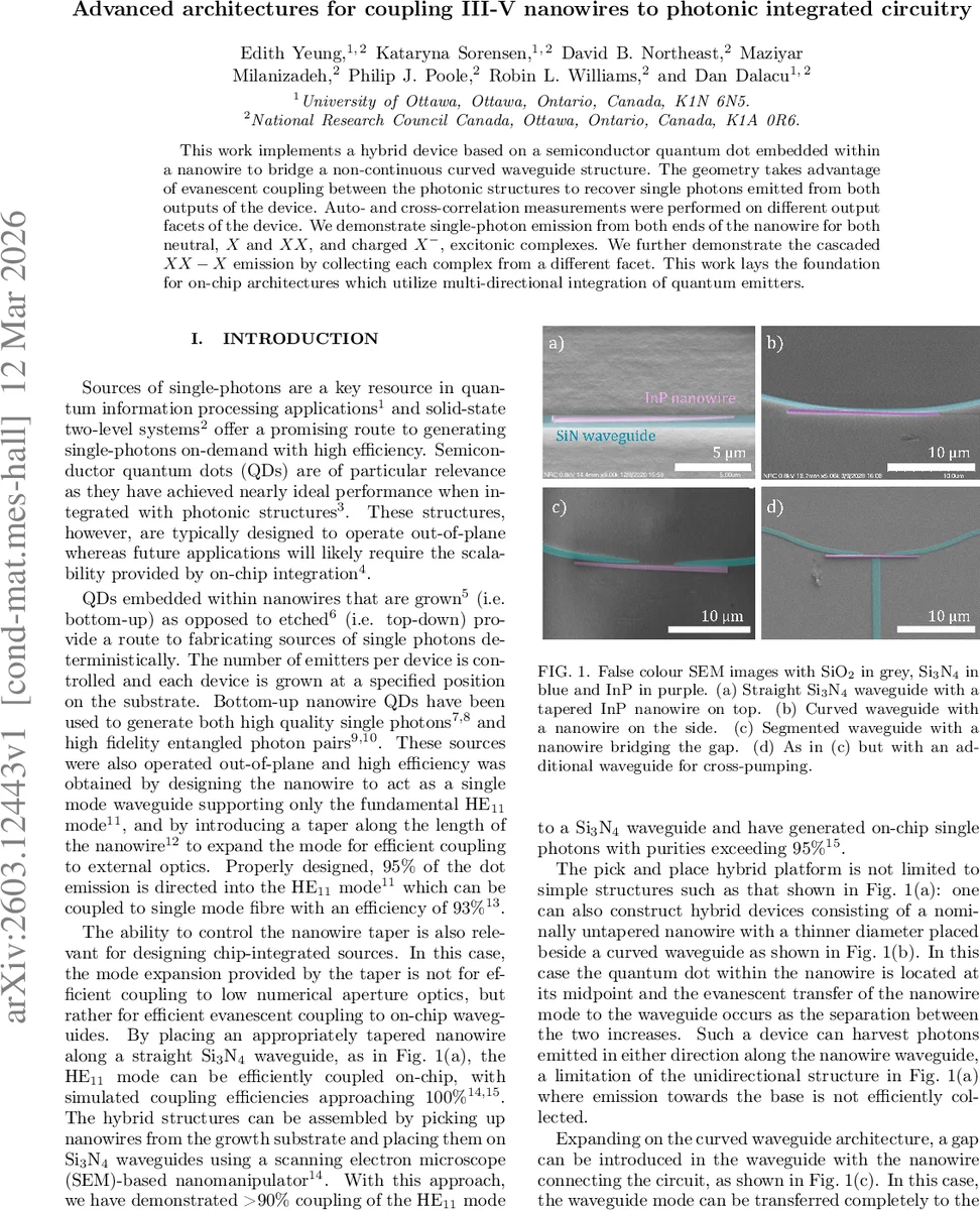
This paper presents a hybrid photonic device that integrates a semiconductor quantum dot (QD) embedded in an InP nanowire with silicon nitride (Si₃N₄) waveguides to achieve efficient, bidirectional single‑photon extraction on a chip. The authors first use finite‑element frequency‑domain simulations (COMSOL) to compare two coupling geometries: (i) a curved Si₃N₄ waveguide directly contacted by the nanowire, and (ii) a segmented waveguide that contains a 4 µm gap bridged by the nanowire, with adiabatic tapers on both sides of the gap. The direct‑contact design shows a peak power transfer of about 76 % for a nanowire radius of 115 nm but is highly sensitive to radius variations. In contrast, the segmented design with tapers yields >90 % transmission for both TE and TM polarizations and is far more tolerant to nanowire diameter fluctuations, because the tapers provide a gradual mode‑size transformation that minimizes abrupt index changes and enhances evanescent coupling.
Experimentally, position‑controlled InAsP QDs are grown inside InP nanowires using selective‑area vapor‑liquid‑solid epitaxy. The nanowires have a 20 nm core, are later clad to a final diameter of 210 nm, and are 20 µm long so that the QD sits at the geometric centre. Using a scanning‑electron‑microscope‑based nanomanipulator, individual nanowires are picked up and placed tangentially across the gap of a Si₃N₄ ridge waveguide (0.4 µm tall, 0.5 µm wide) that features a 30 µm radius curvature and edge‑couplers for fiber access. The final “gap‑coupled” device thus bridges the waveguide gap with the nanowire, positioning the QD exactly in the middle of the gap.
Optical characterization is performed at 5.5 K in a closed‑cycle cryostat. The authors employ three excitation/collection configurations: (i) waveguide‑side pumping and opposite‑side collection, (ii) same‑side pumping and collection using a 90:10 fiber splitter (with optional simultaneous opposite‑side collection), and (iii) free‑space top pumping with collection from both waveguide ends. Continuous‑wave and pulsed (80 MHz, 100 ps) above‑band excitation are used. Emission is filtered with a narrow‑band tunable filter and detected by superconducting nanowire single‑photon detectors (SNSPDs, 80 % efficiency, 100 ps jitter).
Photoluminescence (PL) spectra reveal three dominant lines identified as the neutral exciton (X), biexciton (XX), and charged exciton (X⁻). Under pulsed excitation at saturation, the detected count rates are 575 kcps (X), 330 kcps (XX), and 330 kcps (X⁻), corresponding to end‑to‑end system efficiencies of 0.72 % (X) and 0.41 % (XX, X⁻). The dominant loss originates from the overall optical setup (<10 % throughput) and the fact that only photons propagating toward the collection facet are captured (≈50 % loss). An asymmetry in count rates between the two waveguide ends is observed, likely due to a slight mis‑placement of the QD relative to the gap centre or an unintended taper in the nanowire, which breaks the ideal symmetric coupling predicted by simulations.
Time‑resolved PL measurements show that X and X⁻ exhibit long spin‑flip lifetimes (τ_d ≈ 16–18 ns) together with bright‑state lifetimes (τ_b ≈ 1.7–2.1 ns), whereas XX decays predominantly mono‑exponentially with τ_b ≈ 0.98 ns and a much shorter spin‑flip component. These dynamics are consistent with known relaxation pathways for neutral, charged, and biexcitonic complexes in InAsP QDs.
Second‑order autocorrelation (g²(τ)) measurements performed with a Hanbury‑Brown‑Twiss setup confirm single‑photon emission from all three complexes. At zero delay, g²(0) values are 0.0296 (X), 0.011 (XX), and 0.046 (X⁻). The low g²(0) for X and X⁻ (<5 %) indicates high single‑photon purity, while the higher value for XX (~15 %) is attributed to the higher excitation power needed for biexciton saturation and the faster radiative decay, which increase the probability of re‑excitation within the 100 ps laser pulse.
A key demonstration is the use of the nanowire as an integrated beamsplitter: by collecting photons from both waveguide ends simultaneously, the authors retrieve correlated photon streams from different excitonic complexes (e.g., X from one facet and XX from the opposite facet). This bidirectional operation showcases the potential for multi‑channel quantum photonic circuits where a single quantum emitter can feed several on‑chip pathways.
In summary, the work delivers three major contributions: (1) a systematic design and simulation framework showing that tapered, segmented waveguides dramatically improve evanescent coupling robustness; (2) experimental validation of a gap‑bridging nanowire that provides >90 % simulated coupling and enables bidirectional photon extraction; and (3) comprehensive optical characterization confirming high‑purity single‑photon emission from neutral, charged, and biexcitonic states, with the nanowire acting as an on‑chip beamsplitter. These results constitute a significant step toward scalable integration of III‑V quantum emitters with silicon‑based photonic platforms, opening pathways for on‑chip quantum communication, computing, and sensing architectures that require multi‑directional, low‑loss single‑photon sources.
Comments & Academic Discussion
Loading comments...
Leave a Comment