A Scalable Reconfigurable Intelligent Surface with 3 Bit Phase Resolution and High Bandwidth for 3.6 GHz 5G/6G Applications
Reconfigurable Intelligent Surfaces enable active control of wireless propagation channels, which is crucial for future 5G and 6G networks. This work presents a scalable RIS design operating at 3.6 GHz with both 1 bit and 3 bit phase resolution, supp…
Authors: Markus Heinrichs, Aydin Sezgin, Rainer Kronberger
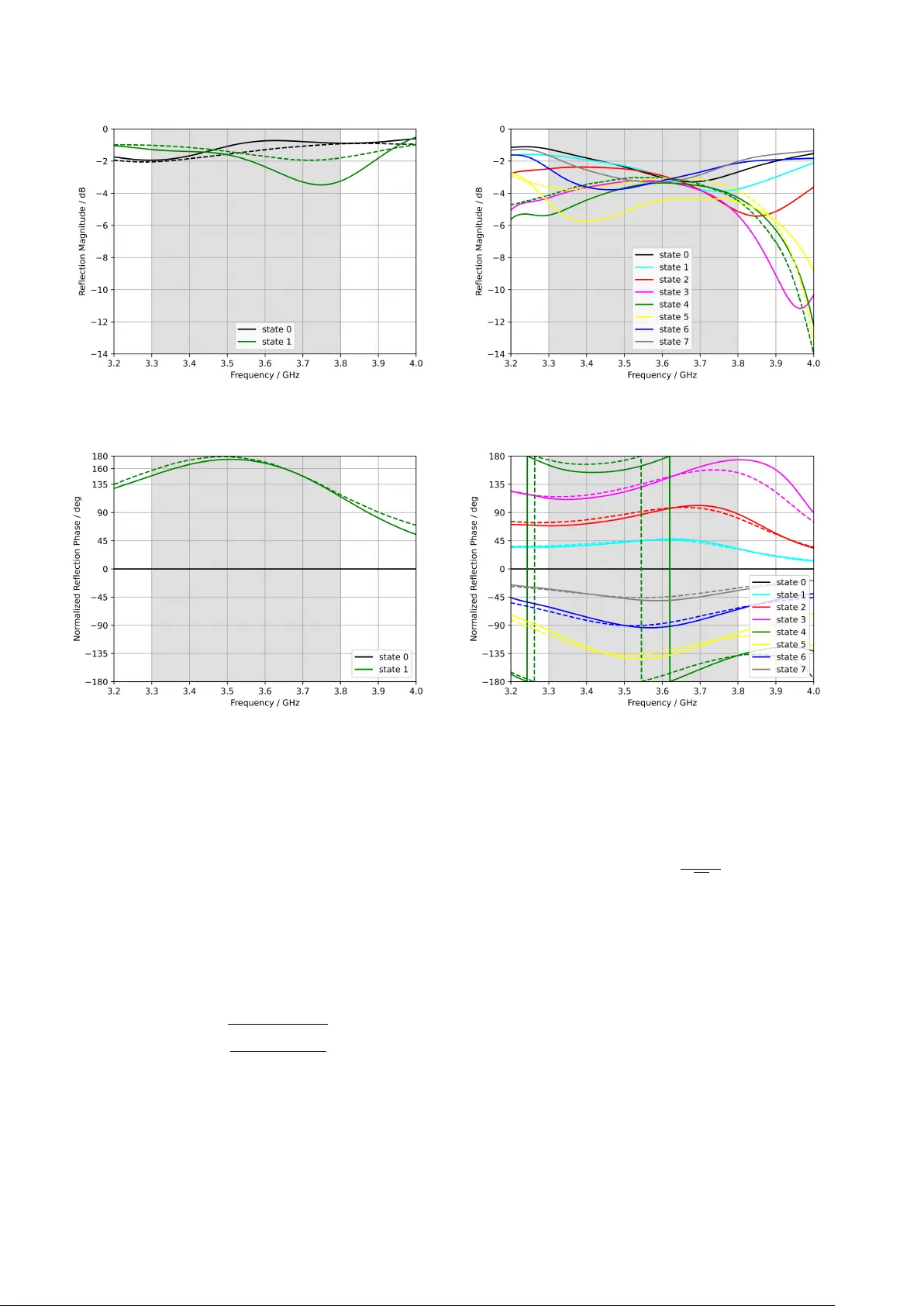
A Scalable Reconfigurable Intelligent Surface with 3 Bit Phase Resolution and High Bandwidth for 3.6 GHz 5G/6G Applications Markus Heinrichs ∗ , A ydin Sezgin † , Rainer Kronberger ∗ ∗ (TH Cologne): High Frequency Laboratory , TH K ¨ oln - Univ ersity of Applied Sciences, Cologne, Germany , markus.heinrichs@th-koeln.de, rainer .kronber ger@th-koeln.de † (Ruhr Univ ersity Bochum): Ruhr Univ ersit ¨ at Bochum, Bochum, Germany , aydin.sezgin@rub.de Abstract —Reconfigurable Intelligent Surfaces enable activ e control of wireless propagation channels, which is crucial for future 5G and 6G networks. This work presents a scalable RIS design operating at 3.6 GHz with both 1 bit and 3 bit phase resolution, supporting wideband applications. The unit cells employ low-cost printed circuit board technology with an innovati ve spring-contact feeding structure, enabling efficient assembly and reduced manufacturing complexity for large-ar ea arrays. The design achieves br oadband phase control, lo w power consumption, and high scalability , with experimental results demonstrating phase tunability across the n78 frequency band and competitive reflection performance compared to existing solutions. This RIS architectur e pr ovides a practical platform for experimental studies of smart radio en vironments, beam steering, and sensing applications in next-generation wireless networks. © 2026 IEEE. Personal use of this material is permitted. Permission from IEEE must be obtained for all other uses, in any current or future media, including reprinting/r epublishing this material for advertising or promotional purposes, creating new collective works, for resale or redistrib ution to servers or lists, or reuse of any copyrighted component of this work in other works. Index T erms —reconfigurable intelligent surface, RIS, intelli- gent reflecting surface, IRS, 6G. I . I N T R O D U C T I O N In 6G networks, controllable radio en vironments—often re- ferred to as smart radio en vironments (SREs)—are considered one of the key innov ations. The goal is to activ ely influence the en vironment in which radio channels are formed, rather than merely adapting to it. Reconfigurable Intelligent Surfaces (RIS) or Intelligent Reflecting Surfaces (IRS) provide the means to achie ve this by allo wing the control of wireless propagation channels. Such surfaces can be used for beam steering, joint communication and sensing (JCS) applications, or to improve the security of communication networks [1]. For the de velopment of such applications, RIS hardware is required to v alidate, test, and improve the proposed concepts under real conditions. This work presents an RIS design for the n78 frequency band at 3.6 GHz, which can be scaled to large-area arrays cov ering several square meters. This enables experimental studies on how RIS structures affect radio channels and propagation en vironments in real-world settings. Additionally , special attention was giv en to minimizing power consumption to ensure usability in large-scale array deployments. The proposed RIS further features a broadband phase response, supporting scientific in vestig ations in wideband 5G and 6G scenarios. In the follo wing section, the proposed unit cell design is introduced, comprising the antenna element and the phase- switching circuits with 1 bit and 3 bit resolution. The imple- mentation of the realized arrays is described in Section III, followed by the measurement in Section IV. The proposed RIS is compared to other designs in Section V before the main findings of this work are summarized in Section VI. I I . U N I T C E L L D E S I G N An RIS consists of an array of identical unit cells, each providing independent control of the reflection phase. Each unit cell comprises an antenna element designed to recei ve the incident free-space wav e that is impinging on the surface and to conv ert it into a conducted wa ve, which is coupled to a microstrip line located on the backside of the unit cell. A circuitry providing an electronically switchable reflection coefficient is connected to the microstrip line port of the antenna. This causes the incident wa ve to be reflected with a phase shift that depends on the switching state of the circuitry . The reflected wave is subsequently re-radiated by the antenna element. T wo types of phase-switching circuits have been dev eloped: one with a 1-bit phase resolution, enabling a 180 ◦ phase change, and another with a 3-bit resolution, allo wing phase control in 45 ◦ steps. A. Antenna Element A linearly polarized rectangular patch antenna was selected as the radiating element. Patch antennas can be fabricated using standard printed circuit board (PCB) technology , which enables cost-ef fectiv e realization in large quantities. As the bandwidth of a patch antenna can be increased by selecting a larger distance between the patch and the ground plane, and to minimize dielectric losses within the substrate, the unit cell’ s antenna is realized using two separate PCBs that are spaced apart by an air gap. The first PCB carries the patch element, while the second PCB serves as the antenna’ s ground plane. T o further reduce manufacturing costs, lo w- cost standard FR4 material has been chosen as the substrate, av oiding the need for more expensi ve RF laminates. The dissipation factor of the FR4 material used is tan δ = 0 . 025 , which is higher than that of commonly used RF materials such as RO4003C ( tan δ = 0 . 0027 ) or RO3003 ( tan δ = 0 . 0010 ) from manufacturer Rogers. Ho wev er , since most of the volume between the patch and the ground plane consists of air , the cost savings achie ved by using FR4 outweigh the increased dielectric losses associated with this material. The spacing between the two PCBs is maintained by 3D- printed spacers that can be snapped into mounting holes provided on both circuit boards. This lo w-cost solution ensures a well-defined and mechanically robust separation between the PCBs while keeping manufacturing and assembly simple and fast. For patch antennas with the feed port located on the backside of the ground plane, a pin feed is commonly used. T ypically , a wire pin is soldered through a hole in the patch on one end and connected to a through-hole pad on the other end. Since the goal is to enable RIS arrays with sev eral hundred elements, manually soldering a wire feed for each unit cell is time-consuming and labor-intensiv e. In addition, pin-fed patch antennas exhibit a high input reactance due to the inductance of the feed pin, which becomes particularly problematic when the spacing between the patch and the ground plane is large. T o address both issues, the wire pin is replaced by a spring contact that is typically used in electromagnetic interference (EMI) shielding applications. This spring contact is a machine- solderable component that can be automatically placed onto the patch PCB. T o compensate for the inductance introduced by the spring contact, it is not connected directly to the patch. Instead, it is soldered on a pad located on the opposite side of the patch PCB, creating a capacitiv e coupling between the patch and the contact pad. The resulting combination forms a series resonant circuit, reducing the reactance of the feeding structure. Fig. 1 sho ws a 3D model of the unit cell as simulated in CST Studio Suite, with a side-view at the bottom. The final dimensions of the optimized unit cell are a width of w uc = 60 . 0 mm , a length of l uc = 45 . 0 mm , a spacing between the patch and the ground plane of d = 5 . 0 mm , a PCB substrate thickness of t = 0 . 8 mm , a patch width of w p = 37 . 0 mm , and a patch length of l p = 30 . 0 mm . This unit cell is used for both versions with 1 bit and 3 bit phase resolution. The material parameters of the FR4 substrate were characterized by measurement, resulting in a relativ e permit- tivity of ε r = 4 . 9 and a dissipation factor of tan δ = 0 . 025 . B. Phase Switching Cir cuits From CST , the simulated S-parameters of the unit cell were exported as a T ouchstone file. Considering the Floquet port as Port 1 and the microstrip line port as Port 2, the overall reflection coefficient of the RIS, Γ RIS i , for a known load reflection coefficient Γ φ i provided by the switching network, is giv en by Γ RIS i = S 11 + S 21 S 12 Γ φ i 1 − S 22 Γ φ i . (1) T o accurately determine the reflection coefficient Γ φ i of the phase-switching circuits, the two RF switches were character- ized using a through-reflect-line (TRL) calibration kit on the same substrate and layer stack-up as used for the final RIS tile. Based on the measured S-parameters of the switches, the circuitry was modeled in Advanced Design System (ADS) to optimize the phase response of the RIS, arg (Γ RIS ) . Fig. 1. CST simulation model of the unit cell showing the feeding structure with an EMI spring contact. FR4 material is rendered in transparent blue. 1) 1-Bit RF Switch: For the 1-bit switch, a SKY A21024 single-pole double-throw (SPDT) RF switch from Skyworks is used. By leaving one port open and connecting the other port to ground, switching between Γ φ 0 = 0 ◦ and Γ φ 1 = 180 ◦ is achiev ed. 2) 3-Bit RF Switch: The 3-bit switch used is a SKY13418- 485LF single-pole eight-throw (SP8T) RF switch, also from Skyworks Inc. T o achie ve phase switching in steps of 45 ◦ , microstrip transmission lines of dif ferent lengths are connected to the eight output ports of the switch, where half of the lines are left open and the other half are terminated to ground. This configuration k eeps the line lengths short, thereby reducing losses and minimizing dispersion effects for a flat phase response ov er frequency . The individual line lengths were optimized in ADS to achiev e reflection coefficients of Γ φ i = i × 45 ◦ for the switching states i = 0 , 1 , . . . , 7 . Fig. 2 shows the simplified schematic of the 3-bit unit cell. state 0 microstrip lines state 1 state 2 state 3 state 4 state 5 state 6 state 7 Γ φ 0 . . . Γ φ 7 [S] antenna 1 2 Γ RIS i Fig. 2. Simplified schematic of the 3 bit unit cell. I I I . R E A L I Z AT IO N For each of the dev eloped unit cells with 1 bit and 3 bit phase resolution, RIS tiles containing 4 × 4 elements were designed and fabricated. Each tile integrates a microcontroller on its back side for configuration of the RIS patterns, allowing multiple tiles to be concatenated into large-scale arrays that cov er multiple square meters of RIS area. T o facilitate experi- ments with the RIS tiles, each unit cell is equipped with a red- green-blue (RGB) LED that indicates its currently configured switching state. The color assignments corresponding to the phase states are listed in T able I and are used consistently in the measurement result plots throughout this paper . T ABLE I C O LO R A S SI G N ME N T . Color Phase Color Phase black 0 ◦ cyan 45 ◦ red 90 ◦ magenta 135 ◦ green 180 ◦ yellow 225 ◦ blue 270 ◦ white 315 ◦ A single 4 × 4 RIS tile of the 3-bit version is sho wn in Fig. 3, where the configured states of each unit cell are indicated by the LEDs visible through the thin FR4 substrate layer . The power consumption of the phase switching circuitry is 2 . 2 mW per tile, excluding the power required by the microcontroller and LEDs. Fig. 3. RIS tile with 16 unit cells and 3 bit phase resolution. For the 1-bit version, an array consisting of 6 × 6 = 36 tiles, corresponding to a total of 24 × 24 = 576 elements, was assembled, resulting in an RIS area of approximately 1 . 56 m 2 . The lar ge-scale array is shown in Fig. 4, where it is mounted on an aluminum truss. The power consumption of the phase switching circuitry of a single 1-bit tile is 0 . 20 mW , resulting in a total po wer consumption of 7 . 2 mW for the complete array of 36 tiles, not accounting for microcontrollers or LEDs. I V . M E A S U R E M E N T S The reflection coefficients of the two RIS versions were experimentally characterized using the horn-antenna setup shown in Fig. 5, where a single RIS tile was positioned in the antenna aperture above RF absorbers. The return loss of the horn antenna was measured with a Streamline P9373A vector network analyzer (VN A) from K eysight to extract the reflection coefficient of the RIS tile, Γ RIS , employing a time- gating procedure to exclude reflections occurring at the coax- to-wa veguide transition of the horn. The measured values were Fig. 4. RIS with 576 unit cells and 1 bit phase resolution, size 1 . 56 m 2 . then normalized to a metallic reference plate of the same size as the RIS tile, providing an absolute magnitude and phase reference. In this way , the mono-static reflection coef ficient for a wav e incident and reflected normal to the RIS surface could be obtained. During the measurement, all 16 unit cells of the RIS tile under test were configured to the same switching state being ev aluated. VNA RIS Fig. 5. Horn antenna measurement setup. The measured magnitude and phase responses of the 1- bit RIS tile are shown in Figs. 6a and 6c, with the n78 frequency band ( 3 . 3 − 3 . 8 GHz in Germany) highlighted in gray . W ithin this band, the lowest magnitude occurs in state 1 and is − 3 . 5 dB . The phase difference between states 0 and 1 remains at least 100 ◦ across the entire 500 MHz n78 band. The measurement results of the 3-bit RIS tile are presented in Figs. 6b and 6d. At the designed center frequency of 3 . 6 GHz , the magnitude response is approximately − 3 . 2 dB for all eight switching states, except for state 5, which exhibits a value of about − 4 . 3 dB . Across the entire n78 band, the lowest magnitude is observed for state 5, reaching − 5 . 75 dB . For improv ed visual clarity , only the simulated magnitude (a) Magnitude response, 1 bit version. (b) Magnitude response, 3 bit version. (c) Phase response normalized to state 0, 1 bit version. (d) Phase response normalized to state 0, 3 bit version. Fig. 6. Magnitude and phase responses of the 1 bit and 3 bit RIS tiles, n78 frequency band highlighted in gray , measurement solid, simulation dashed. responses for state 4 and state 5 are presented, where state 4 exhibits the best agreement between measurement and simula- tion, while state 5 sho ws the largest discrepancy . For the phase, all measured responses agree well with the simulated curves ov er the full operating band. The phase response is optimal at 3 . 60 GHz , where the de viation of the measured normalized phase from the target switching-state phase is minimal. V . C O M PA R I S O N W I T H O T H E R R I S D E S I G N S For comparison of the proposed RIS with existing designs reported in the literature, the bandwidth definition introduced in [2] is adopted. In [2], the standard deviation σ is defined as σ = s P 2 n − 1 i =0 (∆ φ i ) 3 12 × 360 ◦ , (2) where n denotes the number of bits, resulting in 2 n switching states, and ∆ φ i represents the phase dif ference between two adjacent switching states, as illustrated in Figs. 6(c) and 6(d). Based on the standard de viation, the effecti ve number of bits N bit is deriv ed as N bit = log 2 360 ◦ √ 12 σ . (3) As a boundary condition on the phase performance, a min- imum effecti ve bit number of N bit = 1 . 7 bit is used for the 2-bit design in [2]. Consequently , for a 1-bit, 2-bit, and 3-bit RIS, the corresponding minimum effecti ve resolutions are deri ved to be N bit , 1bit = 0 . 7 bit , N bit , 2bit = 1 . 7 bit , and N bit , 3bit = 2 . 7 bit . This results in maximum allowable standard deviations of σ 1bit ≤ 65 ◦ , σ 2bit ≤ 32 . 5 ◦ , and σ 3bit ≤ 16 . 25 ◦ . A. 1-bit V ersion Using the above mentioned bandwidth limit of σ 1bit ≤ 65 ◦ , the usable bandwidth of the 1-bit version is determined to be greater than 500 MHz , covering the whole n78 frequency band. F or comparison, the patch-antenna-based RIS design reported in [3], operating at a center frequenc y of 3 . 5 GHz and fabricated on a lo w-loss RF substrate with a dielectric constant of ε r = 2 . 2 , a dissipation factor of tan δ = 0 . 001 , and a thickness of 2 mm , achieves a bandwidth of 255 MHz with a maximum insertion loss of 4 . 2 dB . In that design, phase switching is implemented using a v aractor diode, and the unit cell size is 30 . 0 mm × 30 . 0 mm . B. 3-bit V ersion Three different RIS designs from the literature were con- sidered for comparison of the 3-bit version. The first design, reported in [4], employs a dipole structure backed by a ground plane as the antenna element. The PCB substrate has a dielectric constant of ε r = 2 . 2 and a dissipation factor of tan δ = 0 . 001 . T wo substrate layers are stacked, resulting in a total thickness of 4 mm between the ground plane and the dipoles. The unit cell dimensions are 30 . 1 mm × 30 . 1 mm . Phase switching is realized using two positiv e- intrinsic-negati ve (PIN) diodes, providing a phase resolution of 2 bit , corresponding to a step size of 90 ◦ . Accordingly , the bandwidth is defined as the frequency range where the standard deviation remains below 32 . 5 ◦ , yielding a bandwidth of approximately 109 MHz . In [5], an RIS design based on a ground plane-backed split con voluted square ring frequency selective surface (FSS) is proposed, with two different versions presented. The first version employs a substrate with a dielectric constant of ε r = 3 . 2 , a dissipation factor of tan δ = 0 . 003 , and a thickness of 1 . 58 mm , combined with an air gap of 1 . 0 mm between the substrate and the ground plane. The unit cell size is 8 . 0 mm × 8 . 0 mm , significantly smaller than the RIS presented in this paper ( 60 mm × 45 mm ) due to the dif ferent operating principle. Phase switching is realized using v aractor diodes. This first version provides 2 bit phase resolution at a center frequency of 3 . 8 GHz , resulting in a usable bandwidth of approximately 190 MHz . The second version is designed for operation at a center frequency of 4 . 2 GHz with a phase resolution of 3 bit . It employs a substrate with a dielectric constant of ε r = 2 . 2 , a dissipation factor of tan δ = 0 . 0009 , and a thickness of 1 . 58 mm , without an air gap. The unit cell size is identical to that of the first version. This second variant provides a usable bandwidth of approximately 85 MHz . When using the above mentioned bandwidth constraints from [2], one has to consider that the allo wable phase de viation is reduced with an increasing phase resolution. Thus, for a valid comparison of the 3-bit RIS presented in this work with 2-bit RIS versions from the literature, the bandwidth of a virtual 2-bit version of the presented RIS is calculated. For this, only the phase states 0, 2, 4 and 6 are considered for computation of the standard deviation. This results in a 2-bit bandwidth of more than 500 MHz , covering the complete span of the n78 band. C. Section Summary As summarized in T able II, the proposed RIS provides a significantly higher bandwidth compared to recent designs in the literature, for all versions with 1 bit , virtual 2 bit , and 3 bit phase resolution. T ABLE II B A N DW I D TH C O M P A R IS O N W I T H T H E L I TE R A T U R E . Unit Cell Frequency Resolution Bandwidth Proposed design 3 . 6 GHz 1 bit > 500 MHz [3] 3 . 5 GHz 255 MHz Proposed design 3 . 6 GHz 2 bit > 500 MHz [4] 3 . 5 GHz 109 MHz [5] 3 . 8 GHz 190 MHz Proposed design 3 . 6 GHz 3 bit 440 MHz [5] 4 . 2 GHz 85 MHz V I . C O N C L U S I O N In this work, a scalable reconfigurable intelligent surface for 3 . 6 GHz 5G/6G applications has been presented. The proposed design supports both 1-bit and 3-bit phase resolution, offering broadband operation across the n78 frequency band. The combination of a patch-antenna-based unit cell with a nov el spring-contact feeding structure enables efficient as- sembly and reduces manufacturing complexity for large-scale arrays. Experimental results demonstrate that the RIS achieves wideband phase tunability with low insertion loss, surpassing the usable bandwidth of comparable designs reported in the literature. The modular tile-based architecture, lo w po wer consumption, and clear visual feedback through RGB LEDs make the design well-suited for experimental studies of smart radio en vironments, beam steering, and sensing applications in next-generation wireless networks. A C K N O W L E D G M E N T This work was funded by the German Federal Ministry of Research, T echnology and Space (BMFTR) in the framew ork of project Reflect6G under grant numbers 16KIS2229 and 16KIS2228K. R E F E R E N C E S [1] M. Di Renzo et al., Smart Radio Envir onments empowered by Reconfig- urable Intelligent Surfaces: how it works, state of resear ch, and the road ahead , in IEEE Journal on Selected Areas in Communications, vol. 38, no. 11, pp. 2450-2525, Nov . 2020, doi: 10.1109/JSAC.2020.3007211. [2] R. Pereira et al., Dual Linearly-P olarized Unit-Cells W ith Nearly 2-Bit Resolution F or Reflectarray Applications In X-Band , in IEEE T ransactions on Antennas and Propagation, vol. 60, no. 12, pp. 6042-6048, Dec. 2012, doi: 10.1109/T AP .2012.2213051. [3] J. Rains et al., Fully-Addressable V aractor -Based Reflecting Metasur- face with Dual-Linear P olarisation for Low P ower Reconfigurable In- telligent Surfaces , 2023 17th European Conference on Antennas and Propagation (EuCAP), Florence, Italy , 2023, pp. 1-5, doi: 10.23919/Eu- CAP57121.2023.10133408. [4] L. Zhu et al., Dual linearly polarized 2-bit pr ogrammable metasurface with high cr oss-polarization discrimination , in IEEE T ransactions on Antennas and Propagation, vol. 72, no. 2, pp. 1510-1520, Feb. 2024, doi: 10.1109/T AP .2023.3345034. [5] S. Dey , A. M. R. M and S. Dey , Novel FSS based multibit passive 8 × 8 RIS for NextGen wir eless communication , 2025 IEEE Wireless Antenna and Microwa ve Symposium (W AMS), Chennai, India, 2025, pp. 1-5, doi: 10.1109/W AMS64402.2025.11158298.
Original Paper
Loading high-quality paper...
Comments & Academic Discussion
Loading comments...
Leave a Comment