Lattice XBAR Filters in Thin-Film Lithium Niobate
This work presents the demonstration of lattice filters based on laterally excited bulk acoustic resonators (XBARs). Two filter implementations, namely direct lattice and layout-balanced lattice topologies, are designed and fabricated in periodically…
Authors: Taran Anusorn, Byeongjin Kim, Ian Anderson
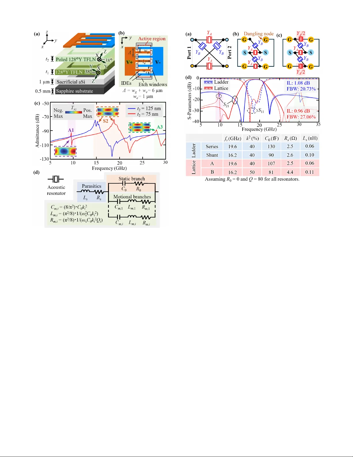
Lattice XB AR Filters in Thin-Film Lithium Niobate T aran Anusorn, Byeongjin Kim, Ian Anderson, Ziqian Y ao, and Ruochen Lu Chandra Family Department of Electrical and Computer Engineering The Univ ersity of T exas at Austin, Austin, TX, USA taran.anusorn@utexas.edu Abstract —This work pr esents the demonstration of lattice fil- ters based on laterally excited bulk acoustic resonators (XBARs). T wo filter implementations, namely direct lattice and layout- balanced lattice topologies, are designed and fabricated in pe- riodically poled piezoelectric film (P3F) thin-film lithium niobate (TFLN). By leveraging the strong electromechanical coupling of XB ARs in P3F TFLN together with the inherently wideband nature of the lattice topology , 3-dB fractional bandwidths (FBWs) of 27.42% and 39.11% and low insertion losses (ILs) of 0.88 dB and 0.96 dB are achieved at approximately 20 GHz for the dir ect and layout-balanced lattice filters, respectively , under conjugate matching. Notably , all prototypes feature compact footprints smaller than 1.3 mm 2 . These results highlight the potential of XB AR-based lattice architectures to enable low-loss, wideband acoustic filters for compact, high-performance RF front ends in next-generation wireless communication and sensing systems, while also identifying key challenges and dir ections for further optimization. Index T erms —Acoustic filter , lattice filter , lithium niobate, periodically-poled piezoelectric film (P3F), XBAR I . I N T RO D U C T I O N M ODERN wireless communications and sensing are in- creasingly data-hungry and perv asiv e, driving the need for compact systems with high power and spectral efficienc y . Among ke y components, acoustic bandpass filters (BPFs) of fer low insertion loss, excellent frequency selectivity , and extreme miniaturization, making them indispensable in modern radio- frequency front ends (RFFEs) operating under multi-standard, spectrum-crowded, and ener gy-constrained environments [1]. Bulk acoustic wave (B A W) filters are strong candidates for applications beyond 6 GHz, where wavelength-scaling limits the operation of surface acoustic wa ve (SA W) filters. Although BA W filters, particularly film bulk acoustic res- onators (FB ARs), are commercially successful, their ultrathin piezoelectric layers, heavy metallization loading, and intrinsic mechanical losses hinder scaling beyond 10 GHz [2]. In contrast, laterally excited bulk acoustic resonators (XBARs) in suspended thin-film lithium niobate (TFLN) enable frequency scaling beyond 10 GHz, and ev en above 100 GHz, while maintaining high electromechanical coupling ( k 2 ) and high quality factor ( Q ) [3]. Owing to the exceptional piezoelectric and anisotropic properties of TFLN, XB AR-based filters hav e This work was supported by the Defense Adv anced Research Projects Agency (D ARP A) under the Compact Front-End Filters at the Element-Level (COFFEE) program No. HR0011-22-2-0031, the National Science Founda- tion (NSF) under CAREER A ward No. 2339731, and the Anandamahidol Foundation Scholarship. Fig. 1. Survey of (a) IL and (b) FBW in acoustic filters above 10 GHz. demonstrated fle xible bandwidth design, low loss, and excel- lent scalability for emerging mobile applications [4]–[11]. Periodically poled film (P3F) TFLN, an engineered lay- ered structure, further enhances k 2 , which directly governs the achiev able fractional bandwidth (FBW), and improves frequency scalability relativ e to single-layer films [12]. A maximum 3-dB FBW of 19.4% has been reported for bi-layer P3F TFLN ladder filters [7]; howe ver , the ladder topology inherently limits further FBW expansion [13]. T o address this constraint, we present the first lattice XBAR filters to the best of our knowledge. T wo lattice filter prototypes exhibit competitiv e insertion loss (IL) and FBW among state-of-the- art acoustic filters beyond 10 GHz [4]–[11], [14]–[17], as summarized in Fig. 1. Furthermore, we built the first practical implementation of a hybrid ladder -lattice XBAR filter . I I . X BA R S I N P 3 F T F L N Follo wing the design methodology in [9], we first study XB ARs in 128 ◦ Y P3F TFLN, as illustrated in Fig. 2(a), using unit-cell finite-element analysis (FEA) in COMSOL Multiphysics. The material ax es X − Y − Z of each TFLN layer are defined relati ve to the de vice coordinates ( x, y , z ) . Notably , the Euler angles for 128 ◦ Y P3F TFLN are (0 , − 38 ◦ , 0) . The dimensions of the interdigitated electrodes (IDEs), including their electrode width ( w e ) and length ( l e ), gap width ( w g ), Fig. 2. (a) Exploded view and (b) top view of an XB AR implemented in bi-layer P3F 128 ◦ Y -cut TFLN, indicating key dimensional parameters (not to scale). (c) Simulated frequency responses of XB AR unit cells with a fixed bottom TFLN thickness of t 1 = 110 nm and varying top-layer thicknesses t 2 ; the corresponding stress mode patterns ( T xz ) are shown adjacent to their associated antiresonances. (d) mBVD model for acoustic resonators exhibiting multiple vibrational modes. and electrode periodicity ( Λ = w e + w g ), of the XBAR are indicated in Fig. 2(b). Fig. 2(c) presents the frequency-domain FEA of the XBAR unit cell with a fixed bottom-layer thickness of t 1 = 110 nm and two different top-layer thicknesses, t 2 = 75 nm and 125 nm. Only symmetric Lamb modes (e.g., S2, S6) can be excited in a P3F platform with uniform layer thickness due to polarity constraints [18]. Nev ertheless, thickness mismatches violate these constraints, thereby exciting antisymmetric modes (e.g., A1, A3). This inherent characteristic directly influences the be- havior of acoustic filters whose frequency scaling is achie ved by trimming only one layer of the P3F stack. T o account for multiple vibrational modes, a modified Butterworth-V an Dyke (mBVD) model with multiple motional branches [Fig. 2(d)] is employed for parameter extraction. I I I . L A T T I C E A C O U S T I C F I LTE R D E S I G N A two-port lattice interconnection of acoustic resonators consists of two identical port-connected resonators Y A and two identical cross-connected resonators Y B [Fig. 3(a)]. The direct lattice design, using planar routing and ground-signal-ground Fig. 3. (a) T wo-port lattice network. Proposed planar-interconnect imple- mentations: (b) direct lattice and (c) layout-balanced lattice configurations. (d) Simulated 50- Ω filter responses based on the mBVD circuit model, with a summary of the design parameters. Dotted S 21 curves illustrate the impact of parasitic A1 and A3 modes on the filter responses. (GSG) probing pads, is sho wn in Fig. 3(b). This layout is inherently asymmetric, resulting in one dangling ground node. T o address this, a layout-balanced configuration is proposed, where one port-connected resonator is divided into two equal sections to form complete connections to all nodes [Fig. 3(c)]. These configurations are equiv alent as long as the admittance between the ground nodes is Y A / 2 . The filter circuits are simulated and optimized in Keysight Advanced Design System (ADS) using the extracted mBVD models of the incorporated resonators under balanced op- eration. T o the best of our knowledge, rob ust analytical synthesis methodologies hav e only been reported for ladder and transversal acoustic filters [19]–[21]; therefore, formal analytical synthesis for lattice acoustic filters is left for future in vestigation. Fig. 3(d) compares the simulated 50- Ω responses of the proposed lattice filters with those of a third-order ladder filter employing two shunt resonators as a reference. The corresponding design parameters are summarized below the plot. Notably , layout-induced parasitics and losses, modeled by R s and L s , are estimated based on prior studies [5]– [9], and only the target S2 mode is initially considered to limit design complexity . For completeness, howe ver , the filter responses under the presence of additional A1 and A3 modes are also simulated and shown as dotted S 21 curves. These results clearly indicate that lattice filters are more susceptible to unwanted modal responses. Despite the spurious sidebands, the lattice filter still outperforms the ladder filter in terms of IL, FBW , and overall out-of-band (OoB) rejection. I V . M E A S U R E D F I L T E R R E S U LT S A N D D I S C U S S I O N S Fabrication is perform on a P3F bi-layer TFLN/aSi/sapphire wafer supplied by NGK Corperation, following the process flow described in [9]. T o tune the resonant frequencies of certain resonators, 50 nm of the top P3F layer is etched via ion milling [22]. IDEs and buslines with a thickness of 350 nm are formed by aluminum (Al) e vaporation, follo wed by an additional 550 nm Al thickening on the buslines to reduce series resistance. T o suspend the active regions of the XBAR devices, release windo ws are first defined by ion milling through both TFLN layers, after which the underlying amorphous silicon (aSi) is selectively removed using XeF 2 to release the active region. A. Dir ect Lattice Filter Fig. 4(a) − (c) shows the fabricated direct lattice filter proto- type with a footprint of 1.15 × 0.81 mm 2 and its standalone resonators A and B, respecti vely . The measured transmission and reflection are shown in Fig. 4(d) and (e), where both S 11 and S 22 are plotted. The measured 50- Ω responses clearly rev eal the asymmetry of this implementation. After applying conjugate matching at each port (30.4 + j 28.2 Ω and 31.1 + j 8.8 Ω for Ports 1 and 2, respecti vely), optimal performance is achiev ed, yielding a minimum IL of 0.88 dB and an FBW of 27% at a center frequenc y ( f c ) of 19.7 GHz. It is worth noting that the optimal complex matching impedance at each port is determined from Z 0 ,i = Z 0 1 + Γ m,i 1 − Γ m,i , (1) where the optimal reflection coef ficient Γ m,i is giv en by Γ m,i = B i − p B 2 i − 4 | C i | 2 2 C i , (2) with B i = 1 + | S ii | 2 − | S j j | 2 − | ∆ | 2 , (3) C i = S ii − ∆ S ∗ j j , (4) and ∆ = S 11 S 22 − S 12 S 21 . (5) Here, i, j ∈ { 1 , 2 } with i = j [23]. The measured admittance of each standalone resonator is shown in Fig. 4(f), together with the extracted mBVD model parameters. Although the extracted C 0 is close to the design value, modeling and parameter estimation inaccuracies lead to minor discrepancies between the simulated and the measured. In addition, the induced A1 and A3 modes in resonator A contribute to undesirable filter sidebands. Notably , the extracted R s and R 0 values may indicate elev ated resistive losses, potentially arising from thin buslines due to damage to the thickened Al layer during the lift-off process and from ion- milling-induced damage in the TFLN, respectively . Howe ver , these parameters are obtained solely through curve fitting, and dedicated inv estigations are required to assess how accurately they reflect the underlying physical loss mechanisms. Fig. 4. (a) Fabricated direct lattice filter and its standalone resonators: (b) A and (c) B, indicating the number N e and length l e of the IDEs. Measured (d) transmission and (e) reflection responses of the prototype filter . (f) Measured admittance of the resonators along with the extracted mBVD model parameters, considering only the S2 mode; the influence of each mode is highlighted. B. Layout-Balanced F ilter The fabricated layout-balanced lattice filter prototype, with a footprint of 1.29 × 0.85 mm 2 , along with its constituent resonators A1, A2, and B, is sho wn in Fig. 5(a) − (d). The measured transmission and reflection are presented in Fig. 5(e) − (f). Notably , the symmetric layout enables a more practical implementation of matching networks. W ith conju- gate matching applied, the filter achieves a minimum IL of 0.96 dB and a wide FBW of 39%, highlighting the adv antages of the lattice topology . A different f c of 17.7 GHz in this implementation is attributable to local variations in the wafer’ s LN thickness. Nev ertheless, in addition to unwanted responses induced by the A1 and A3 modes, imperfect resonator splitting (i.e., Fig. 5. (a) Fabricated layout-balanced lattice filter and its standalone res- onators: (b) A1, (c) A2, and (d) B, indicating the number N e and length l e of the IDEs. Measured (e) transmission and (f) reflection responses of the prototype filter . (g) Measured admittance of the resonators along with the extracted mBVD model parameters, considering only the S2 mode; the influence of each mode is highlighted. Y A 1 = 2 Y A 2 ), as illustrated in Fig. 5(g), results in an undesir- able roll-up in S 21 , as highlighted in Fig. 5(e). Furthermore, the series-resonance peak locations of XBARs shift with resonator size, e ven when the series-resonance frequency f s is identical, due to layout-induced electromagnetic resonances. This effect introduces an additional challenge in the accurate modeling and design of XBAR filters at mmW av e [8], [9], [11]. T echniques and in-depth analyses to mitigate these effects and further optimize the performance of the layout- balanced lattice configuration will be explored in future work. V . C O N C L U S I O N This work presents the first practical implementation of lattice XBAR filters. The measurement demonstrates the po- tential of acoustic filters with low IL and wide FBW at fre- quencies abov e 18 GHz. The results also rev eal that practical challenges arise from accurate modeling of acoustic de vices in the presence of EM resonance, de vice fabrication, and the synthesis of feasible filters that account for such nonideali- ties. W ith continued efforts, the proposed design could yield compact, high-performance RF front-end solutions for next- generation wireless communication and sensing applications. A C K N O W L E D G M E N T The authors thank Dr . Ben Griffin, Dr . T odd Bauer , Dr . Zachary Fishman, Dr . Tzu-Hsuan Hsu, Dr . Harshv ardhan Gupta, Dr . Omar Barrera, and Mr . Jack Kramer for their helpful and inspiring discussions. R E F E R E N C E S [1] A. Hagelauer et al. , “From microw ave acoustic filters to millimeter-w ave operation and new applications, ” IEEE J. Micr owaves , vol. 3, no. 1, pp. 484-508, Jan. 2023. [2] V . Chulukhadze et al. , ”T o ward miniature high-coupling lithium niobate thin-film bulk acoustic wav e resonators at millimeter wave, ” IEEE TED , Feb . 2026. [3] R. Lu, “Recent advances in high-performance millimeter-W ave acoustic resonators and filters using thin-film lithium niobate, ” Pro g. Quantum Electr on. , May 2025. [4] L. Gao, Y . Y ang, and S. Gong, “Wideband hybrid monolithic lithium niobate acoustic filter in the K-Band, ” IEEE TUFFC , 2021. [5] O. Barrera et al. , “Thin-film lithium niobate acoustic filter at 23.5 GHz with 2.38 dB IL and 18.2% FBW , ” IEEE J. MEMS , Dec. 2023. [6] O. Barrera et al. , “Transferred thin film lithium niobate as millimeter wav e acoustic filter platforms, ” in Proc. MEMS , 2024. [7] S. Cho et al. , “23.8-GHz acoustic filter in periodically poled piezo- electric film lithium niobate with 1.52-dB IL and 19.4% FBW , ” IEEE MWTL , April 2024. [8] O. Barrera et al. , “38.7 GHz thin film lithium niobate acoustic filter , ” in Proc. IMFW , 2024. [9] T . Anusorn et al. , “Practical demonstrations of FR3-Band thin-film lithium niobate acoustic filter design, ” IEEE TUFFC , Dec. 2025. [10] O. Barrera et al. , ”19.3 GHz acoustic filter with high close-in rejection in tri-layer thin-film lithium niobate, ” IEEE EDL , Dec. 2025 [11] O. Barrera et al. , “50 GHz piezoelectric acoustic filter, ” IEEE J. Microw . , accepted . [12] J. Kramer and R. Lu, “ A generalized acoustic framework for multilayer piezoelectric platforms, ” IEEE TUFFC , Sept. 2025. [13] J. Heighway , S. N. Kondratiev and V . P . Plessky , “Balanced bridge SA W impedance element filters, ” in Pr oc. IUS , 1994. [14] A. Kochhar et al. , “X-band bulk acoustic wav e resonator (XBA W) using periodically polarized piezoelectric films (P3F), ” in Proc. IUS , 2023. [15] C. Liu et al. , “Up to 48 GHz mmW av e ferroelectric SC0.3Al0.7N bulk acoustic wave resonators and filters, ” in Proc. IEDM , 2024. [16] Izhar et al. , “Periodically poled aluminum scandium nitride b ulk acoustic wav e resonators and filters for communications in the 6G era, ” Micr osyst. Nanoeng. , Jan. 2025. [17] M. M. A. Fiagbenu et al. , ”A high-selectivity 11.9-GHz filter realized in a periodically poled piezoelectric AlScN film, ” IEEE MWTL , Oct. 2025. [18] R. Lu, Y . Y ang, S. Link and S. Gong, ”Enabling higher order Lamb wav e acoustic devices with complementarily oriented piezoelectric thin films, ” IEEE J. MEMS , Oct. 2020. [19] S. Cano, L. Acosta, C. Caballero, J. V erd ´ u, and P . de Paco, ”Synthesis of wideband filters based on acoustic wav e transversal and ladder topologies, ” in Pr oc. IC-MAM , 2024. [20] S. Cano, et al. , ”General synthesis methodology for acoustic wave ladder filters in the bandpass domain, ” IEEE TMTT , Oct. 2025. [21] S. Cano, J. V erd ´ u and P . de Paco, ”Coupling matrix decomposition of acoustic wa ve ladder filters in the bandpass domain, ” IEEE TMTT , Jan. 2026. [22] V . Chulukhadze et al. , “Frequency scaling millimeter wa ve acoustic resonators using ion beam trimmed lithium niobate, ” in Pr oc. IFCS , 2023. [23] D. M. Pozar , Microwa ve engineering. Hoboken, Nj: W iley , 2012.
Original Paper
Loading high-quality paper...
Comments & Academic Discussion
Loading comments...
Leave a Comment