EM-Aware Physical Synthesis: Neural Inductor Modeling and Intelligent Placement & Routing for RF Circuits
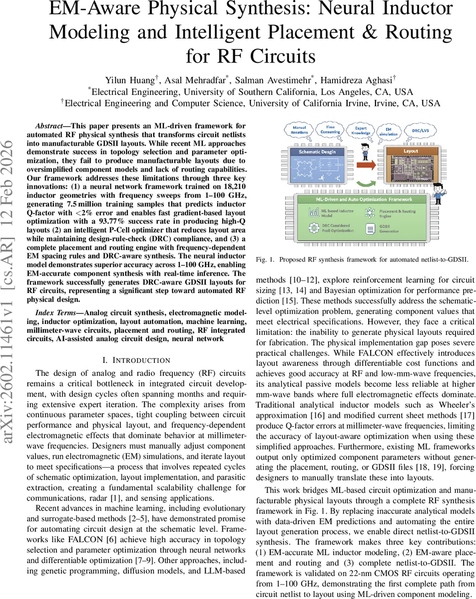
This paper presents an ML-driven framework for automated RF physical synthesis that transforms circuit netlists into manufacturable GDSII layouts. While recent ML approaches demonstrate success in topology selection and parameter optimization, they fail to produce manufacturable layouts due to oversimplified component models and lack of routing capabilities. Our framework addresses these limitations through three key innovations: (1) a neural network framework trained on 18,210 inductor geometries with frequency sweeps from 1-100 GHz, generating 7.5 million training samples, that predicts inductor Q-factor with less than 2% error and enables fast gradient-based layout optimization with a 93.77% success rate in producing high-Q layouts; (2) an intelligent P-Cell optimizer that reduces layout area while maintaining design-rule-check (DRC) compliance; and (3) a complete placement and routing engine with frequency-dependent EM spacing rules and DRC-aware synthesis. The neural inductor model demonstrates superior accuracy across 1-100 GHz, enabling EM-accurate component synthesis with real-time inference. The framework successfully generates DRC-aware GDSII layouts for RF circuits, representing a significant step toward automated RF physical design.
💡 Research Summary
The paper introduces a comprehensive, EM‑aware machine‑learning (ML) driven physical synthesis flow that converts RF circuit netlists directly into manufacturable GDSII layouts. The authors identify two major gaps in existing ML‑based analog design tools: (1) reliance on simplified analytical models for passive components, which become inaccurate at millimeter‑wave frequencies, and (2) the inability to generate physical placement, routing, and DRC‑compliant layouts. To close these gaps, the work presents three tightly coupled innovations.
First, a neural‑network surrogate for inductor quality factor (Q) is trained on a massive dataset of 7.5 million samples derived from full‑wave electromagnetic (EM) simulations of 18,210 distinct inductor geometries across 1 – 100 GHz. The model is a ten‑layer multilayer perceptron (MLP) with ReLU activations, LayerNorm, and a Softplus output to enforce non‑negative Q. Training uses Adam (lr = 0.001, batch = 16 384) with early stopping; on a held‑out test set it achieves MAE 0.419, RMSE 0.65, R² 0.994, and MAPE 1.36 %, corresponding to less than 2 % error over the entire frequency band.
Second, the trained forward model is frozen and employed in a gradient‑based inverse design loop (inspired by the “gradient reasoning” approach of FALCON). Given fixed specifications—target frequency f, metal width W, and inductance L—the layout parameters (vertical length Lv, horizontal length Lh, and center length LCN) are treated as differentiable variables. The loss is simply the negative predicted Q, and Adam (lr = 0.01) updates the layout variables while clamping them to feasible physical bounds. Over 3 000 optimization steps (typically under one second on a standard laptop CPU) the method achieves a 93.77 % success rate for Q > 10, demonstrating that the surrogate can drive rapid, high‑performance layout synthesis without any additional EM simulations.
Third, the flow integrates an intelligent P‑Cell optimizer, a frequency‑aware placement engine, and a global routing engine that respects both foundry design‑rule checks (DRC) and EM spacing rules. The P‑Cell optimizer enumerates metal‑stack options for capacitors, sheet‑resistance models for resistors, and geometric variations for inductors, selecting the minimum‑area solution that meets electrical targets within ±0.5 % tolerance. Placement minimizes a cost function consisting of half‑perimeter wire length (HPWL) plus a heavy overlap penalty, using connectivity‑driven ordering, local swaps, translations, and rotation scoring based on pin‑escape space. Frequency‑dependent minimum spacing is stored in an EM rule database; guard‑band margins of 10‑20 % are applied to mitigate substrate coupling and crosstalk.
Routing is performed on a 0.1 µm grid using an A* algorithm. The cost function combines accumulated path cost, Manhattan distance to the target, and a large penalty for layer switches to discourage excessive via usage. A minimum spanning tree (MST) defines net topology, and routing respects DRC‑derived forbidden regions as well as EM‑aware clearance halos that expand with frequency. Pin escape is handled in two phases (straight escape followed by dogleg if needed), ensuring no‑over‑cell violations.
The final GDSII generation stage assembles the optimized device geometries and routed interconnects into hierarchical layout files via the Python gdstk library, interfacing directly with the foundry PDK. The authors demonstrate the flow on a Class‑B power amplifier, producing a complete layout (though transistor devices are represented as simplified three‑pin boxes, a limitation acknowledged for future work).
A comparative table shows that, unlike prior works (e.g., CKTGNN, LaMA‑GIC, AnalogCoder, LayoutCopilot), this approach simultaneously supports automated layout generation, EM‑aware design, RF/mm‑wave frequency ranges, foundry PDK integration, and public datasets/code.
In conclusion, the presented EM‑aware ML‑driven physical synthesis pipeline achieves sub‑2 % Q‑factor prediction error, fast gradient‑based layout optimization with a 93.77 % high‑Q success rate, area‑efficient P‑Cell generation, and DRC‑compliant placement and routing. It reduces RF design cycles from weeks to minutes and opens the door to real‑time design space exploration. Remaining challenges include handling transistor layout symmetry/mirroring, scaling to densely packed analog blocks, and extending the methodology to nonlinear RF components such as VCOs and PLLs.
Comments & Academic Discussion
Loading comments...
Leave a Comment