From Buffers to Registers: Unlocking Fine-Grained FlashAttention with Hybrid-Bonded 3D NPU Co-Design
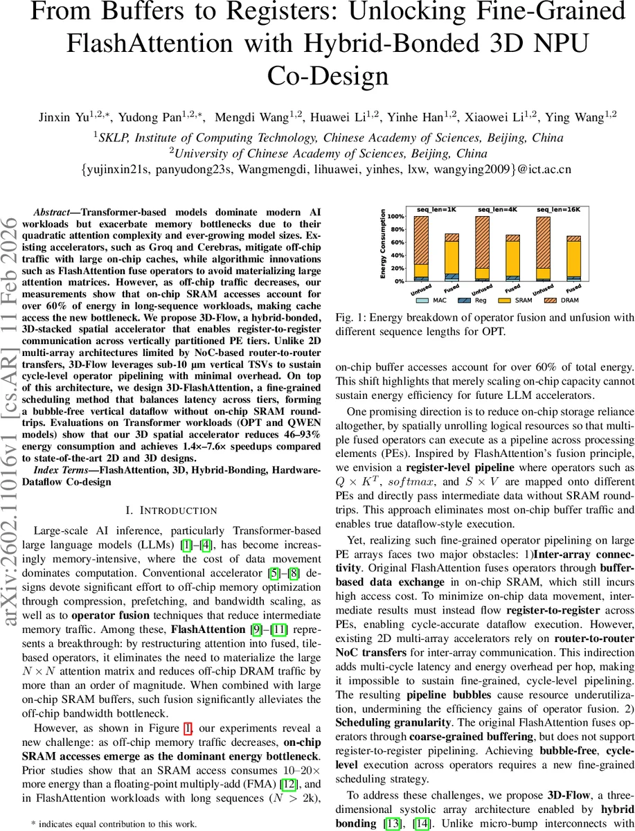
Transformer-based models dominate modern AI workloads but exacerbate memory bottlenecks due to their quadratic attention complexity and ever-growing model sizes. Existing accelerators, such as Groq and Cerebras, mitigate off-chip traffic with large on-chip caches, while algorithmic innovations such as FlashAttention fuse operators to avoid materializing large attention matrices. However, as off-chip traffic decreases, our measurements show that on-chip SRAM accesses account for over 60% of energy in long-sequence workloads, making cache access the new bottleneck. We propose 3D-Flow, a hybrid-bonded, 3D-stacked spatial accelerator that enables register-to-register communication across vertically partitioned PE tiers. Unlike 2D multi-array architectures limited by NoC-based router-to-router transfers, 3D-Flow leverages sub-10 um vertical TSVs to sustain cycle-level operator pipelining with minimal overhead. On top of this architecture, we design 3D-FlashAttention, a fine-grained scheduling method that balances latency across tiers, forming a bubble-free vertical dataflow without on-chip SRAM roundtrips. Evaluations on Transformer workloads (OPT and QWEN models) show that our 3D spatial accelerator reduces 46-93% energy consumption and achieves 1.4x-7.6x speedups compared to state-of-the-art 2D and 3D designs.
💡 Research Summary
The paper addresses a newly emerging bottleneck in transformer inference: as off‑chip DRAM traffic is reduced by techniques such as FlashAttention, on‑chip SRAM accesses become dominant, accounting for more than 60 % of the total energy in long‑sequence workloads (N > 2 k). The authors first quantify this shift through detailed energy breakdowns on existing 2D systolic‑array accelerators (e.g., Groq, Cerebras) and demonstrate that the conventional buffer‑based data exchange used by FlashAttention still incurs substantial SRAM traffic and suffers from load imbalance between the matrix‑multiply intensive Q·Kᵀ stage and the comparatively slower softmax‑related stages.
To overcome these limitations, the authors propose 3D‑Flow, a hybrid‑bonded, three‑dimensional stacked processing‑element (PE) architecture. By leveraging sub‑10 µm pitch through‑silicon‑via (TSV) links enabled by hybrid bonding, vertically adjacent PE tiers are connected directly at the register level, providing a one‑cycle, low‑energy data path. Each tier is specialized for a particular sub‑operation of FlashAttention: Layer 0 performs Q·Kᵀ with an outer‑stationary MAC array, Layer 1 computes row‑max via comparators and subtractors, Layer 2 handles exponentiation and row‑sum, and Layer 3 executes the P·V multiplication and output scaling. This vertical partitioning eliminates the need to write intermediate results to on‑chip SRAM, thereby removing the SRAM round‑trip overhead entirely.
On top of this hardware substrate the authors introduce 3D‑FlashAttention, a fine‑grained scheduling algorithm that balances the latency of each sub‑operation across the four tiers. By modeling the cycle cost of each operator and aligning them so that every tier finishes its work in the same number of cycles, a bubble‑free pipeline is achieved. When the pipeline is fully populated, a single FlashAttention iteration (processing a d × d tile) completes in 2 d cycles, compared with the 3 d cycles required merely for the Q·Kᵀ step on a conventional 2D array. This represents a ≈33 % reduction in per‑iteration latency and enables sustained high utilization of all compute resources.
Thermal analysis of a 128 × 128 PE array stacked in four layers shows a modest power density of ≈41 W cm⁻² and an estimated temperature rise of only 2.8 °C, confirming that the vertical TSV network also provides effective heat conduction. With a realistic package thermal resistance (RθJA ≈ 2.5 K W⁻¹), the junction temperature remains well below typical safety limits even at peak power (≈13 W total).
The authors evaluate the full system on real‑world large language models (OPT‑1.3B, QWEN‑7B) across a range of sequence lengths (1 k, 4 k, 16 k). Compared to state‑of‑the‑art 2D designs and recent 3D HBM‑stack accelerators, 3D‑Flow with 3D‑FlashAttention achieves 46 %–93 % reduction in energy consumption and 1.4×–7.6× speed‑up. Notably, for the longest sequences the SRAM‑access proportion in baseline designs spikes, yet the proposed architecture maintains a bubble‑free pipeline and delivers consistent performance gains.
In summary, the paper makes three key contributions: (1) a rigorous bottleneck analysis showing that on‑chip SRAM traffic now dominates energy in long‑sequence transformer inference; (2) the design of a hybrid‑bonded 3D‑stacked PE architecture that enables register‑to‑register vertical dataflow with sub‑cycle latency; and (3) a latency‑balanced scheduling scheme that maps FlashAttention’s sub‑operators onto the vertical tiers, eliminating SRAM round‑trips and achieving bubble‑free execution. This hardware‑algorithm co‑design demonstrates a viable path to substantially improve the energy efficiency and throughput of future LLM inference accelerators.
Comments & Academic Discussion
Loading comments...
Leave a Comment