Interplay of Defects and the Charge Density Wave State in Hf-Doped ZrTe$_{3}$
We carry out temperature-dependent scanning tunneling microscopy (STM) studies of the charge density wave (CDW) compound ZrTe$3$ which is intentionally doped with Hf. Previous bulk studies tie Hf doping to an enhancement of the CDW transition temperature (T${CDW}$). In our work, by combining STM measurements with density functional theory (DFT) calculations, we observe and identify multiple defects in Zr${0.95}$Hf${0.05}$Te$3$. Surprisingly, instead of finding clear structural or electronic signatures associated with Hf dopants, we determine the origin of the observed defects are consistent with Te and Zr vacancies. Further, our temperature dependent STM measurements allow us to examine CDW pinning to both types of observed defects below and above T${CDW}$.
💡 Research Summary
In this work the authors investigate the charge‑density‑wave (CDW) material ZrTe₃ that has been intentionally doped with 5 % hafnium (Zr₀.₉₅Hf₀.₀₅Te₃). Using temperature‑dependent scanning tunneling microscopy (STM) from 9 K (well below the CDW transition temperature, T_CDW ≈ 63 K) up to 92 K (above T_CDW), they map the atomic surface, the CDW modulation, and the presence of defects. Contrary to expectations that Hf atoms substituting for Zr would produce a clear electronic or structural signature, the STM images reveal two recurring types of linear defects that persist over the whole temperature range.
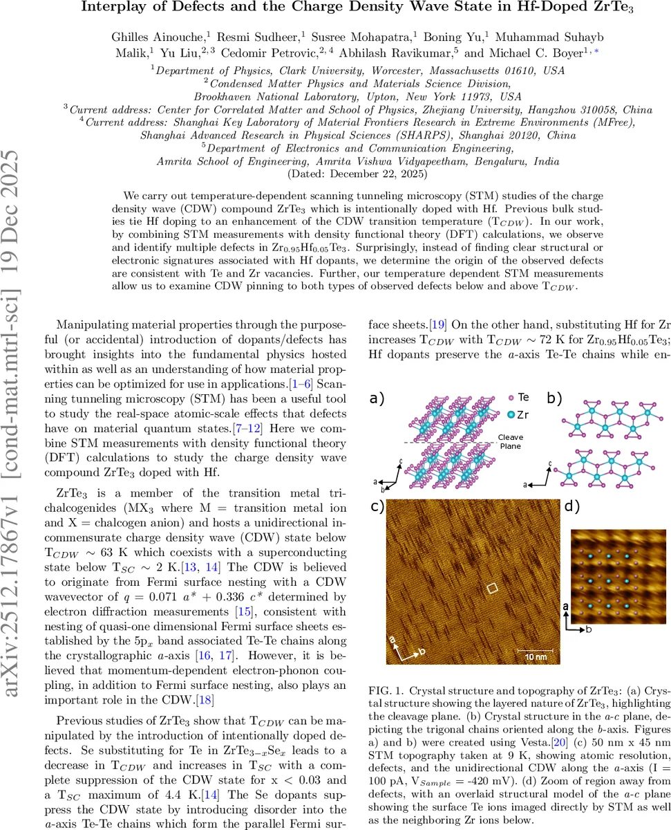
The first type, termed “Extended Dark Defect” (EDD), appears as a dark line extending along the a‑axis for roughly 14–15 unit cells while being confined to a single unit cell along the b‑axis. Line‑cut analysis shows a shallow depression in the topography and, uniquely at the defect centre, a single peak instead of the usual double‑peak associated with the two inequivalent surface Te atoms (Te(2) and Te(3)). Density‑functional theory (DFT) calculations in which a surface Te atom is removed reproduce exactly this feature: the missing Te creates a local vacancy, the remaining Te atom relaxes toward the centre, and the simulated STM image (via the Tersoff‑Hamann approach) matches the experimental dark line. Hence the EDDs are identified as surface Te vacancies.
The second type, “Extended Bright Defect” (EBD), is a bright line also aligned with the a‑axis but spanning about 12 unit cells and two unit cells along the b‑axis. Unlike the EDD, the EBD shows no obvious lattice distortion in the line cuts, suggesting a subsurface origin. The authors first test the hypothesis that the bright defect could be an Hf atom substituting for Zr. DFT simulations of an Hf‑substituted Zr site show virtually no change in the surface electronic density, and the simulated STM image is indistinguishable from that of a pristine surface. Therefore Hf substitution cannot account for the observed bright defect.
Subsequent DFT modeling of a Zr vacancy beneath the surface reproduces the bright, slightly raised topography, the subtle central depression, and a modest distortion of the four surrounding surface Te atoms. The simulated STM image of a Zr vacancy aligns closely with the experimental EBD, confirming that the bright defects correspond to subsurface Zr vacancies.
Fourier‑transform analysis of the STM topographies yields a CDW wave vector q_CDW ≈ 0.07 a*, in agreement with earlier electron‑diffraction and X‑ray measurements. By comparing images taken below and above T_CDW, the authors show that the CDW amplitude diminishes with temperature but remains locally pinned at defect sites. In the vicinity of Te vacancies, the CDW phase is strongly perturbed, indicating that these vacancies act as robust pinning centers that lock the CDW phase. Zr vacancies also pin the CDW, but the effect is weaker and appears to arise from a local modification of the electronic potential rather than a large structural distortion.
The study demonstrates that the enhancement of T_CDW reported for Hf‑doped ZrTe₃ is not a direct consequence of Hf substitution; instead, the presence of intrinsic Te and Zr vacancies—defects that are introduced unintentionally during crystal growth—plays a dominant role in modifying the CDW. Te vacancies disrupt the a‑axis Te‑Te chains that form the quasi‑one‑dimensional Fermi‑surface sheets responsible for nesting, thereby affecting electron‑phonon coupling and stabilizing the CDW at higher temperatures. Zr vacancies, being subsurface, modify the local electronic environment without strongly breaking the chains.
Overall, the combination of high‑resolution STM, temperature‑dependent measurements, and first‑principles simulations provides a comprehensive picture of how specific point defects interact with a collective electronic order. The work underscores the importance of distinguishing intentional dopants from accidental vacancies when interpreting doping effects in low‑dimensional CDW materials, and it offers a methodological blueprint for future studies of defect‑engineered quantum phases.
Comments & Academic Discussion
Loading comments...
Leave a Comment