Effect of substrate miscut angle on critical thickness, structural and electronic properties of MBE-grown NbN films on c-plane sapphire
We report the structural and electronic properties of niobium nitride (NbN) thin films grown by molecular beam epitaxy on c-plane sapphire with miscut angles of $0.5^\text{o}$, $2^\text{o}$, $4^\text{o}$, and $10^\text{o}$ towards m-axis. X-ray diffraction (XRD) scans reveal that the full width at half maximum of the rocking curves around the 1 1 1 reflection of these NbN films decreases with increasing miscut. Starting from 76 arcsecs on $0.5^\text{o}$ miscut, the FWHM reduces to almost 20 arcsecs on $10^\text{o}$ miscut sapphire indicating improved structural quality. Scanning transmission electron microscopy (STEM) images indicate that NbN on c-sapphire has around 10 nm critical thickness, irrespective of the substrate miscut, above which it turns columnar. The improved structural property is correlated with a marginal increment in superconducting transition temperature $T_\text{c}$ from 12.1 K for NbN on $0.5^\text{o}$ miscut sapphire to 12.5 K for NbN on $10^\text{o}$ miscut sapphire.
💡 Research Summary
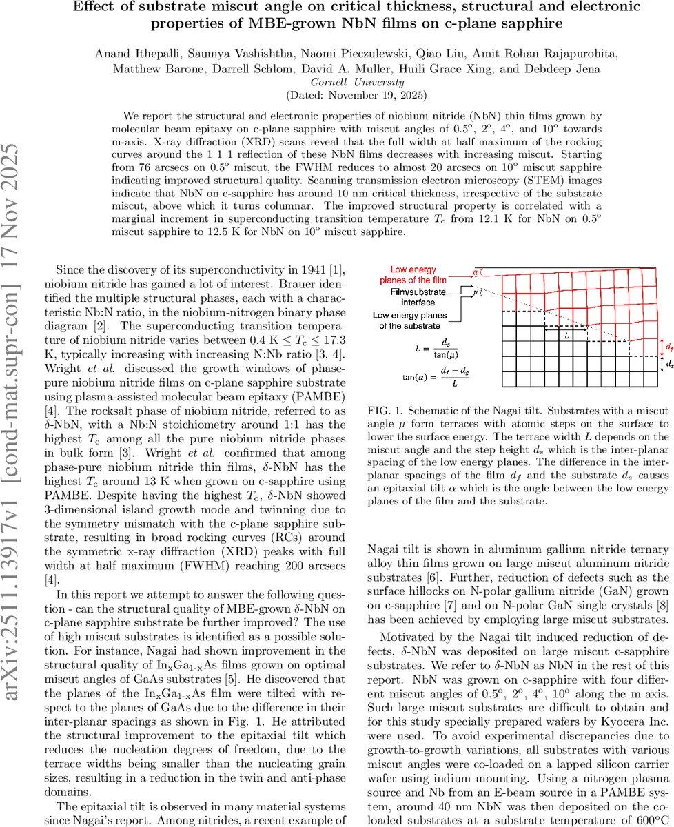
In this work the authors investigate how the miscut angle of c‑plane sapphire substrates influences the structural and electronic properties of epitaxial niobium nitride (NbN) thin films grown by plasma‑assisted molecular beam epitaxy (P‑MBE). Four substrates were prepared with miscut angles of 0.5°, 2°, 4°, and 10° toward the sapphire m‑axis, and a ~40 nm δ‑NbN layer was deposited on all of them under identical conditions (600 °C substrate temperature, nitrogen plasma source, Nb effusion cell).
X‑ray diffraction (XRD) measurements show a systematic narrowing of both the 2θ‑ω peak and the ω rocking curve (RC) of the NbN (111) reflection as the miscut increases. The full‑width at half‑maximum (FWHM) of the 2θ‑ω peak drops from 727.2 arcsec for the 0.5° sample to 57.6 arcsec for the 10° sample, while the RC FWHM decreases from 76 arcsec to 20 arcsec. This trend indicates a reduction of mosaic spread and micro‑strain in the films. A Williamson‑Hall analysis reveals that the peak broadening is dominated by strain (β ∝ ε) rather than crystallite size, suggesting that larger miscut angles relieve lattice mismatch strain, possibly by facilitating the formation of a Nagai tilt. The measured tilt angles (≈0.1° for 0.5° miscut and ≈2° for 10° miscut) agree with the theoretical values derived from the difference between the inter‑planar spacings of sapphire (ds = 0.216 nm) and NbN (df ≈ 0.254 nm).
Scanning transmission electron microscopy (STEM) provides a direct view of the film morphology. Regardless of miscut, the NbN remains a coherent, single‑crystal layer up to a critical thickness of about 10 nm; beyond this thickness the film transitions to a columnar growth mode. High‑angle annular dark‑field (ADF) and integrated differential phase contrast (iDPC) images show that the sapphire/NbN interface is atomically sharp, and misfit dislocations with a density of ~1.6 × 10¹² cm⁻² are present at the interface for all samples. The dislocation density does not vary with miscut, confirming that the observed improvement in XRD metrics is not due to a reduction in misfit dislocations but rather to strain relaxation and tilt.
Electrical transport was measured in a Van der Pauw geometry. The room‑temperature resistivity is essentially independent of the substrate miscut, reflecting the dominance of electron‑phonon scattering at 300 K. The residual resistivity ratio (RRR = ρ300 K/ρ13 K) shows a modest increase from 0.59 (0.5° and 4°) to 0.62 (10°), consistent with a slight reduction of defect scattering. The superconducting transition temperature Tc, extracted from the normalized resistance versus temperature curves, rises from 12.1 K for the 0.5° sample to 12.5 K for the 10° sample—a 0.4 K (≈3 %) enhancement. The authors note that the Tc spread in a control set of four identical 0.5° miscut samples is only 0.2 K, indicating that the observed Tc increase is reproducible and not an artifact of sample‑to‑sample variation.
In summary, increasing the sapphire miscut angle up to 10° markedly improves the crystalline quality of δ‑NbN films, as evidenced by narrower XRD rocking curves and reduced lattice strain. However, the critical thickness for the onset of columnar growth, the density of interfacial misfit dislocations, and the overall electronic transport (room‑temperature resistivity, RRR) remain largely unchanged. The modest Tc enhancement suggests that while structural perfection is beneficial, the columnar morphology and associated grain boundaries still limit the ultimate superconducting performance.
The authors propose several future directions: (i) systematic comparison of sub‑10 nm and >10 nm NbN layers to isolate the impact of columnar boundaries on transport; (ii) exploration of alternative miscut directions (e.g., a‑axis) or different sapphire orientations such as r‑plane, which may further reduce defects; (iii) growth of other transition‑metal nitrides that do not form columnar structures on c‑sapphire to disentangle the role of miscut‑induced strain from morphology. These avenues could lead to NbN films with both superior structural integrity and enhanced superconducting properties, which are crucial for quantum‑computing and high‑frequency detector applications.
Comments & Academic Discussion
Loading comments...
Leave a Comment