An Embedded RISC-V Core with Fast Modular Multiplication
💡 Research Summary
The paper addresses the challenge of providing efficient public‑key cryptography on power‑constrained IoT end‑nodes. While software implementations of elliptic‑curve cryptography (ECC) are flexible, they consume significant energy and latency. Dedicated hardware accelerators deliver speed but lack adaptability to future algorithmic changes. To balance flexibility, area, and power, the authors extend a minimal in‑order RV32EC RISC‑V core with a custom instruction called MMUL that performs Montgomery modular multiplication directly in hardware.
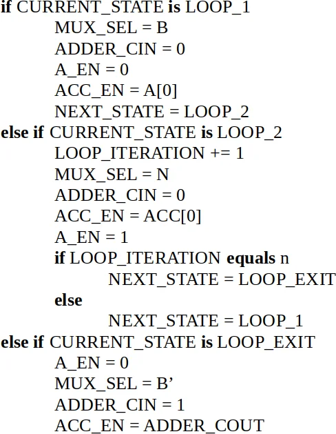
The MMUL instruction encodes three memory addresses (multiplicand, multiplier, modulus) and the operand length. After evaluating several RISC‑V instruction formats, the designers chose the R4‑type format because it imposes no restrictions on operand layout, simplifying software integration. The hardware implementation follows the radix‑2 Montgomery multiplication (R2MM) algorithm, which consists solely of additions and shifts. For an n‑bit operation the hardware requires 2 n + 1 clock cycles plus memory loads and stores, where each iteration of the algorithm consumes two cycles.
A key contribution is the “partial execution” mode. In the default atomic mode (CI‑AE) the processor stalls for the entire duration of the MMUL operation, which can be problematic for real‑time IoT tasks. By writing a flag to a dedicated CSR (CSR3), the core switches to partial execution (CI‑PE). In this mode the MMUL instruction processes a single bit of the operands, retires, and returns control to the core, allowing interrupts and other tasks to be serviced between bits. The software must invoke MMUL n times for an n‑bit multiplication, but the latency per call drops to a few memory cycles, and loop unrolling can make the overall execution time comparable to the atomic case while preserving responsiveness.
The authors evaluate the design on both FPGA (Xilinx XC7Z020) and ASIC (TSMC 0.18 µm) platforms. The 128‑bit MMUL runs at 81 MHz on FPGA and 136 MHz on ASIC. Compared with a baseline RV32EC core (BA) that performs all operations in software, the custom instruction yields speed‑ups of 9‑13× on four ECC benchmarks: FourQ (128‑bit), NIST P‑256, Curve25519 (both 256‑bit), and the ARIS authentication scheme. Dynamic power consumption drops dramatically: the ASIC implementation reduces dynamic power from 0.154 W (BA) to 0.064 W (CI‑AE) and 0.120 W (CI‑PE), corresponding to up to 95 % overall energy savings for the larger curves.
Area overhead is modest: the FPGA core grows from 487 to 649 slices (≈33 % increase) and the ASIC core from 8 106 gates to 12 105 gates (≈49 % increase). Clock frequency decreases by about 8‑9 % due to the added datapath. Nevertheless, the energy‑per‑operation advantage outweighs the modest area and frequency penalties. The authors also compare their results with prior work on lightweight block‑cipher acceleration on RISC‑V, which reported around 58 % area overhead, highlighting the efficiency of their approach.
In conclusion, the paper demonstrates that a carefully designed custom instruction for Montgomery multiplication can dramatically accelerate ECC on ultra‑low‑power RISC‑V cores while preserving the ability to update algorithms in software. The partial‑execution scheme solves the real‑time responsiveness issue without sacrificing most of the performance gain. Future work may extend the concept to other modular operations such as exponentiation, explore multi‑core coordination, and support larger operand sizes to broaden applicability across diverse IoT security scenarios.
Comments & Academic Discussion
Loading comments...
Leave a Comment