Machine Learning Based Image Calibration for a Twofold Time-Interleaved High Speed DAC
In this paper, we propose a novel image calibration algorithm for a twofold time-interleaved DAC (TIDAC). The algorithm is based on simulated annealing, which is often used in the field of machine learning to solve derivative free optimization (DFO) …
Authors: Daniel Beauchamp, Keith M. Chugg
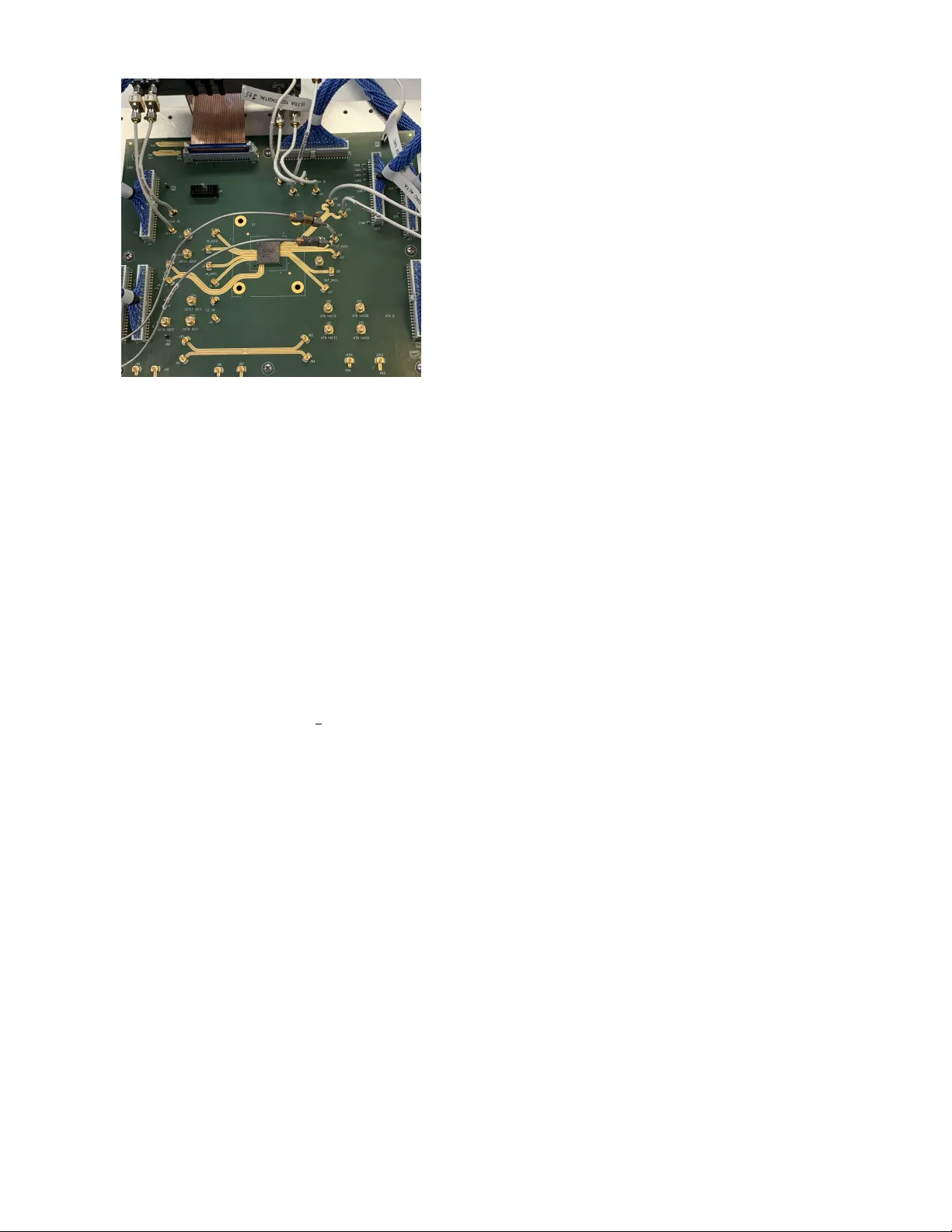
Machine Learning Based Image Calibration for a T wofold T ime-Interlea v ed High Speed D A C Daniel Beauchamp ∗ † and K eith M. Chugg † ∗ Jariet T echnologies, 103 W T orrance Blvd, Redondo Beach, CA 90277 † Ming Hsieh Department of Electrical Engineering, Univ ersity of Southern California, Los Angeles, California 90089 { dbeaucha, chugg } @usc.edu Abstract —In this paper , we propose a novel image calibration algorithm for a tw ofold time-interlea ved DA C (TID A C). The algorithm is based on simulated annealing, which is often used in the field of machine learning to solve derivati ve-free optimization (DFO) problems. The digital-to-analog con verter (D A C) under consideration is part of a digital transceiver core that contains a high speed analog-to-digital conv erter (ADC), microcontroller , and digital control via a Serial Peripheral Interface (SPI). These are used as tools for designing an algorithm which suppresses the interleav e image to the noise floor . The algorithm is supported with experimental results in silicon on a 10-bit twofold TID A C operating at a sample rate of 50 GS/s in 14nm CMOS technology . I . I N T R O D U C T I O N Con ventional radio-frequency (RF) front-ends are typically composed of sev eral mixers, local oscillators and analog filters. These components are a sizeable expense in terms of cost, area, and power , especially when implemented in phased array systems with sev eral radiating antenna elements [1]. Fortunately , integrated circuit technology has adv anced to such a degree that con ventional RF front-end solutions are being replaced with high speed ADCs, D A Cs and digital signal processing (DSP) which perform frequency conv ersion and filtering operations in the digital domain [2]. This allows data conv erters to be placed closer to the antenna, thereby significantly reducing system cost and power consumption. In addition, high speed con verters have their thermal and quantization noise power spread across a wide Nyquist zone, which enhances dynamic range after processing gain. In order for data con verters to achieve multi-GS/s rates, it is common to time-interleav e sev eral low speed conv erters [3], [4]. The high speed of the TID AC coupled with the area efficiency inherent in 14nm CMOS presents an ideal use case for phased array systems such as next generation radar and 5G. Howe ver , the inevitable timing errors and mismatch among the lo w speed conv erter slices results in images, or spectral replicas, which corrupt the conv erter output spectrum. Therefore, image calibration schemes are often necessary in order to a void considerable loss of dynamic range. The authors in [4] consider a 20 GS/s 6-bit DA C with no calibration scheme in place. As a result, the spurious- free dynamic range (SFDR) is limited to 40 dB at output frequencies near 9 GHz. The authors in [5] consider a twofold delta sigma TIDA C operating at an aggregate sample rate of 10 GS/s. The clock duty cycle error is understood to be the limiting impairment reg arding dynamic range, and calibration schemes are proposed. Howe ver , the recommended solution in volv es digital pre-filtering, which is essentially equiv alent to increasing the D AC resolution and tightening matching requirements. Although an analog post-correction scheme is proposed, an accurate measurement of clock duty cycle is required, and this proves to be increasingly challenging at higher sample rates. In [6], the issue of the interleave image is recognized as a limiting factor in high speed TIDA C performance. A self- calibration circuit is proposed, but it is only functional for sample rates belo w 200 MS/s. Calibration schemes above this rate are left as an opportunity for future research. The authors in [7] pro vide a duty-cycle calibration algorithm for a twofold TID AC, but assume that the sub-DA C slices are balanced in terms of gain. Practically , this is not a valid assumption for an RF D A C in deep sub-micron processes. In fact, ev en minor mismatch in sub-DA C gain can exacerbate the interleave image, leading to major loss of dynamic range. This is shown in Section II. In this paper , we consider a 10-bit twofold TID AC with current steering architecture operating at an aggregate rate of 50 GS/s using two 25 GS/s sub-D AC slices in 14nm CMOS technology . The D AC is part of a digital transceiv er core from Jariet T echnologies that contains an on-chip high speed ADC, microcontroller, and digital control via an SPI interface. For the DA C under consideration, there is an image which appears at half of the aggregate sample rate. As far as we know , calibration schemes for D A Cs at sample rates this high have not been reported. As shown in Section II, the impairments which exacerbate this image are clock duty cycle error , mismatch in sub-D AC analog gain, and clock and data misalignment. W e use the closed-loop configuration shown in Fig. 1 to design an algorithm which suppresses the interleave image to the noise floor . This ensures that dynamic range does not suf fer due to interleaving effects. Note that although the authors in [7] use a similar configuration to Fig. 1, the algorithm proposed herein does not assume the sub-D A Cs are balanced in terms of gain. In addition, the configuration in Fig. 1 does not rely on any bandwidth limited circuitry as in [6], and does not tighten matching requirements as in [5]. Fig. 1: Block diagram of the TIDA C in a closed loop config- uration. In Section II, we provide some background information on twofold TIDA Cs. Using Fourier analysis, we explicitly show how specific impairments can cause an undesired image at half of the aggregate sample rate. In Section III, we concretely define the problem at hand in an integer programming frame- work, and a novel solution is proposed based on simulated annealing. In Section IV , we apply this solution to a 50 GS/s D A C in 14nm CMOS and provide experimental results which highlight its efficac y in terms of image suppression. W e conclude in Section V by summarizing the ke y results and providing some direction for future research. I I . T W O F O L D T I M E - I N T E R L E A V E D DA C The block diagram for the general M -bit TID AC operating at a sample rate of f s is illustrated in Fig. 2. Fig. 2: Simplified block diagram of the TID AC, the fractional timing error , α , shown in lower right. A phase locked loop (PLL) generates a clock at frequency f s / 2 which is distributed to the blocks denoted by serializer, sub-D A C A, sub-D AC B, and AMUX. The serializer contains a clock tree with se veral 2-to-1 multiplexers that serialize the N low speed parallel lanes into two high speed ones at the f s / 2 rate. The sub-D A C slices employ current drivers for each bit to con vert the M -bit code presented at the input to an analog output current. The driv ers are composed of binary weighted current sources and clock driven switches. When the switches are activ e, current is driv en to the output, and when they are inactive, current is dumped to a dummy node which is not shown in the diagram. This is controlled by the analog multiplex er (AMUX). Ideally , in this ping-pong like configuration, each sub- D A C driv es current to the output for 50% of the half-rate clock period. Howe ver , this is generally not the case due to unav oidable clock duty cycle error . In Fig. 2, we include a fractional timing of fset factor α ∈ [ − 1 , 1] in order to account for this. Note that α = 0 corresponds to the ideal case of 50% duty cycle. In this section, we show that this impairment causes an image in the frequency domain which is located at f s / 2 . Also shown in Fig. 2 are the sub-D AC analog gains, g A and g B . Note that in general, g A 6 = g B mainly due to current source imbalance between the sub-D ACs, and this also causes an image at f s / 2 . W e refer to the architecture illustrated in Fig. 2 as a current steering twofold TID AC. W e proceed by computing Y ( f ) , which is the Fourier transform of the D A C output y ( t ) . Throughout the paper, we denote the Fourier transform of a time-domain signal y ( t ) by Y ( f ) = Z ∞ −∞ y ( t ) e − j 2 πf t dt. (1) Note that y ( t ) = y A ( t ) + y B ( t ) , (2) so we can compute the Fourier transform of the individual sub-D A Cs and then simply add the result to obtain Y ( f ) by linearity of the Fourier transform. W ithout loss of generality , assume that sub-D A C A is driving current to the output at time t = 0 . Note that y A ( t ) can be modeled as a sum of phase shifted return-to-zero (RZ) pulses whose amplitude is determined by the discrete-time sequence x A ( n ) = x (2 nT s ) , where x ( t ) is the continuous-time representation of the input. In particular , we hav e y A ( t ) = g A Π t − T s 2 (1 + 2 α ) T s (1 + 2 α ) ! ∗ x ( t ) · ∞ X k = −∞ δ ( t − 2 k T s ) ! (3) where Π( t ) := 0 if | t | > 1 2 1 if | t | = 1 2 1 if | t | < 1 2 (4) δ ( t ) is the Dirac delta function, and ∗ denotes the conv olution operator . It is clear that (3) is a sum of phase shifted RZ pulses, as it is the con volution of a rectangular function with an impulse train. T aking the Fourier transform of (3), we hav e Y A ( f ) = g A 2 (1 + 2 α ) sinc ( f T s (1 + 2 α )) e − j πf T s (1+2 α ) × ∞ X k = −∞ X f − k f s 2 (5) where sinc ( x ) := sin( π x ) / ( π x ) , and we use the fact that con volution in the time domain becomes multiplication in the frequency domain and vice-versa. The Fourier transform of y B ( t ) is obtained similarly , and is given by Y B ( f ) = g B 2 (1 − 2 α ) sinc ( f T s (1 − 2 α )) e − j πf T s (1 − 2 α ) × ∞ X k = −∞ X f − k f s 2 e − j πk (1+2 α ) (6) Note the additional complex exponential factor in the sum of (6) compared to (5) due to the assumption that sub-DA C A is aligned at t = 0 . Using (2), the Fourier transform of the DA C output y ( t ) is Y ( f ) = Y A ( f ) + Y B ( f ) (7) where Y A ( f ) and Y B ( f ) are gi ven by (5) and (6) respecti vely . Note that if α = 0 , the complex exponential in the sum of (6) is -1 for k odd and will cancel the the corresponding term in (5) if and only if g A = g B . As mentioned in the introduction, clock and data misalignment also exacerbates the f s / 2 image. Fig. 3: Illustration of clock and data alignment for a twofold TID A C. When sub-D AC A undergoes a data transition, there is a settling window of τ settle as shown in Fig. 3. During this time, sub-D A C A is dumping current to the dummy node while sub- D A C B is dri ving current to the output. The ideal scenario corresponds to the case where the clock edges are equidistant from the data transitions as illustrated in Fig. 3. In any other scenario, one sub-DA C has a longer (or shorter) τ driv e than the other . It is this timing imbalance which exacerbates the image at f s / 2 in a manner similar to that of clock duty cycle error . For the chip under consideration in Section IV , there is an algorithm that performs coarse clock and data alignment, b ut that is beyond the scope of this paper . Consider a twofold TID AC for the case in which the ideal output is a sinusoid at frequency f out . From inspection of (7), there is an interlea ve spur which appears at f s / 2 − f out . The contour plots in Fig. 4 illustrate the -50 dBc lev el curves of the interleav e spur magnitude for v arious v alues of f out . These are obtained using (7). If the gain and duty cycle errors are contained within these contours on the lower left region of Fig. 4, then we guarantee the image spur is less than -50 dBc, which is reasonable from an SFDR perspecti ve for a wideband RF D AC. From Fig. 4 it is clear that extremely small gain and duty cycle errors are required for reasonable DA C SFDR performance. In Section III, we propose a machine learning based algo- rithm which uses digital control to suppress the interleave spur to the noise floor . Fig. 4: -50 dBc le vel curves of interleave image magnitude when the ideal output is a sinusoid at frequency f out . I I I . S I M U L AT E D A N N E A L I N G A L G O R I T H M As mentioned in the introduction, the D A C under consid- eration is part of a digital transceiv er core that contains a high speed ADC and digital control via a microcontroller and SPI interface. There are several controls which remedy the impairments discussed in Section II. T able I outlines these controls along with their corresponding objectiv es. Note that the chip under consideration in Section IV has these controls split into six different control registers, each of which has a wide range of discrete settings. Therefore, we begin by defining a state v ector s ∈ S ⊂ R 6 whose entries are composed of the digital control settings. In order to find the optimal control settings, we require the ability to measure the interleav e spur power . Consider a TIDA C with sample rate f s and sinusoidal output with frequenc y f out . Again, by inspection of (7), we observ e that an interlea ve spur appears at f s / 2 − f out . Using the on-chip ADC, we then sample the D A C output, compute the fast Fourier Transform (FFT), and monitor the bin corresponding to f s / 2 − f out . The energy in this FFT bin then defines a cost function C : S → R . The objectiv e is to then choose a vector s ∗ ∈ S such that s ∗ = arg min s C ( s ) (8) The objectiv e defined by (8) is an integer programming problem. There are a couple of ke y items worth mentioning. First, note that we do not hav e an expression for the cost function C ( s ) , so optimization via relaxation and dif feren- tiation is not an option. In addition, the solution space is Digital control Objectiv e sub-D AC output current g A → g B f s / 2 clock duty cycle α → 0 Phase rotator τ settle ≈ τ drive for both sub-DA Cs T ABLE I: List of digital controls with corresponding objec- tiv es. large, as the state vector lies in six-dimensional space and each entry has a wide range of discrete values. A suitable algorithm which promotes global optimum conv ergence in this scenario is known as simulated annealing [8]. The pseudocode for simulated annealing is outlined in Algorithm 1. Algorithm 1: Simulated annealing. Input: s 0 , T max , T min , γ , β , K Output: s ∗ 1 s ← s 0 2 s ∗ ← s 3 T ← T max 4 while T > T min do 5 for k ← 0 to K − 1 do 6 s 0 ← n ( s ) 7 ∆ E ← C ( s 0 ) − C ( s ) 8 if ∆ E ≤ 0 then 9 s ← s 0 10 if C ( s ) < C ( s ∗ ) then 11 s ∗ ← s 12 else if rand (0 , 1) < exp − β ∆ E T then 13 s ← s 0 14 T ← γ T Algorithm 1 has a temperature parameter T which starts high at T max and gradually reduces to T min exponentially with factor γ . At each value of T , we perform K iterations which inv olve a cost comparison of the current state s with a neighboring state s 0 = n ( s ) . Note that states s 0 whose cost is less than or equal to the current state s are always accepted (i.e. ∆ E ≤ 0 ). If a neighbor is accepted under the criteria ∆ E ≤ 0 , then we check whether or not it has a lower cost than the optimal state s ∗ . Howe ver , states with higher cost (i.e. ∆ E > 0 ) are not necessarily rejected. In fact, the acceptance of higher cost states is controlled by the temperature T in a probabilistic manner . Note that the term exp − β ∆ E T → 1 as T → ∞ where β > 0 is a hyperparameter . This implies that the state space is explored aggressively when T is large since the acceptance of higher cost states becomes more probable. A key component of Algorithm 1 inv olves constructing the neighboring state function n ( s ) . In our case, this process first in volv es choosing a number from the discrete uniform distribution U { 1 , 6 } which corresponds to one of the six digital controls. W e then choose another number uniformly at random over a range which cov ers the selected control setting. The neighbor state is found by simply substituting the new control setting into a copy of the pre vious state. I V . E X P E R I M E N TA L R E S U LTS In this section, we use the Agilent N9030A spectrum analyzer to apply Algorithm 1 to a 10-bit twofold 50 GS/s TID A C in 14nm CMOS. Note that the spectrum analyzer samples the D A C output which effecti vely emulates the on- chip ADC. Fig. 5: Interleav e spur performance over Nyquist. The plot in Fig. 5 demonstrates the efficac y of Algorithm 1 ov er Nyquist and compares it to a simple grid search over the state space. Note that Algorithm 1 keeps the interleave spur well below -50 dBc. After starting Algorithm 1 with control registers in their initial states, conv ergence occurs after an av erage of 160 interleav e spur measurements, and grid search was performed with 280 measurements. Note that at high frequency , simulated annealing has a 15 dB improv ement over grid search while requiring nearly half as many measurements. The parameters used as input to Algorithm 1 were γ = 0 . 8 , K = 30 , and β = 50 . These experiments were conducted using an Altera FPGA which serves as a bridge between the PC and the SPI interface. The test board and chip are shown in Fig. 6. V . C O N C L U S I O N In this paper , a novel image calibration algorithm for a twofold TID AC is proposed and verified in silicon on a 10- bit 50 GS/s D A C in 14nm CMOS. The algorithm does not exacerbate matching requirements as in [5], and does not assume the sub-D A C gains are balanced as in [7]. Furthermore, bandwidth limited calibration circuitry is not required as in [6]. Although an on-chip high speed ADC is assumed, this is becoming much more practical with the use of low po wer deep sub-micron processes like 14nm CMOS. Future work inv olves repeating the measurements in Section IV using the on-chip D A C to ADC loopback path. Beyond interleave impairments, high speed data con verters have harmonic distortion. Using machine learning for harmonic suppression would be another interesting and fruitful research opportunity . Fig. 6: T est board with digital transceiv er chip containing a 50 GS/s TID A C. A C K N O W L E D G M E N T The authors would like to Jariet T echnologies for providing the financial support and equipment which made this research possible. R E F E R E N C E S [1] C. G. Tsinos, S. Maleki, S. Chatzinotas, and B. E. Ottersten, “Hybrid analog-digital transceiv er designs for cogniti ve large-scale antenna array systems, ” CoRR , vol. abs/1612.02957, 2016. [Online]. A vailable: http://arxiv .org/abs/1612.02957 [2] R. Levinson, C. Hornbuckle, and K. Dyer, “ A monolithic analog to digital con verter in 32nm CMOS for broadband phased array applications, ” in 2013 IEEE International Conference on Micr owaves, Communications, Antennas and Electr onic Systems (COMCAS 2013) , Oct 2013, pp. 1–13. [3] M. El-Chammas and B. Murmann, T ime-Interleaved ADCs . New Y ork, NY : Springer New Y ork, 2012, pp. 5–30. [Online]. A v ailable: https://doi.org/10.1007/978- 1- 4614- 1511- 4 2 [4] S. Kim, W . Kim, M. Seo, and S. Ryu, “ A 65-nm CMOS 6-bit 20 GS/s time-interleav ed D AC with full-binary sub-D ACs, ” IEEE T ransactions on Cir cuits and Systems II: Express Briefs , vol. 65, no. 9, pp. 1154–1158, Sep. 2018. [5] A. Bhide and A. Alvandpour , “Timing challenges in high-speed inter- leav ed D A Cs, ” in 2014 International Symposium on Integr ated Circuits (ISIC) , Dec 2014, pp. 46–49. [6] B. Jankunus, “Design and calibration of a 12-bit current-steering D AC using data-interleaving, ” 2014. [7] E. Olieman, A. Annema, and B. Nauta, “ An interleaved full nyquist high- speed D AC technique, ” IEEE J ournal of Solid-State Cir cuits , vol. 50, no. 3, pp. 704–713, March 2015. [8] L. M. Rios and N. V . Sahinidis, “Deriv ative-free optimization: a review of algorithms and comparison of software implementations, ” Journal of Global Optimization , vol. 56, no. 3, pp. 1247–1293, 07 2013.
Original Paper
Loading high-quality paper...
Comments & Academic Discussion
Loading comments...
Leave a Comment