An open and flexible digital phase-locked loop for optical metrology
This paper presents an open and flexible digital phase lock loop optimized for laser stabilization systems. It is implemented on a cheap and easily accessible FPGA-based digital electronics platform (Red Pitaya) running a customizable open-source fir…
Authors: Alex Tourigny-Plante, Vincent Michaud-Belleau, Nicolas Bourbeau-Hebert
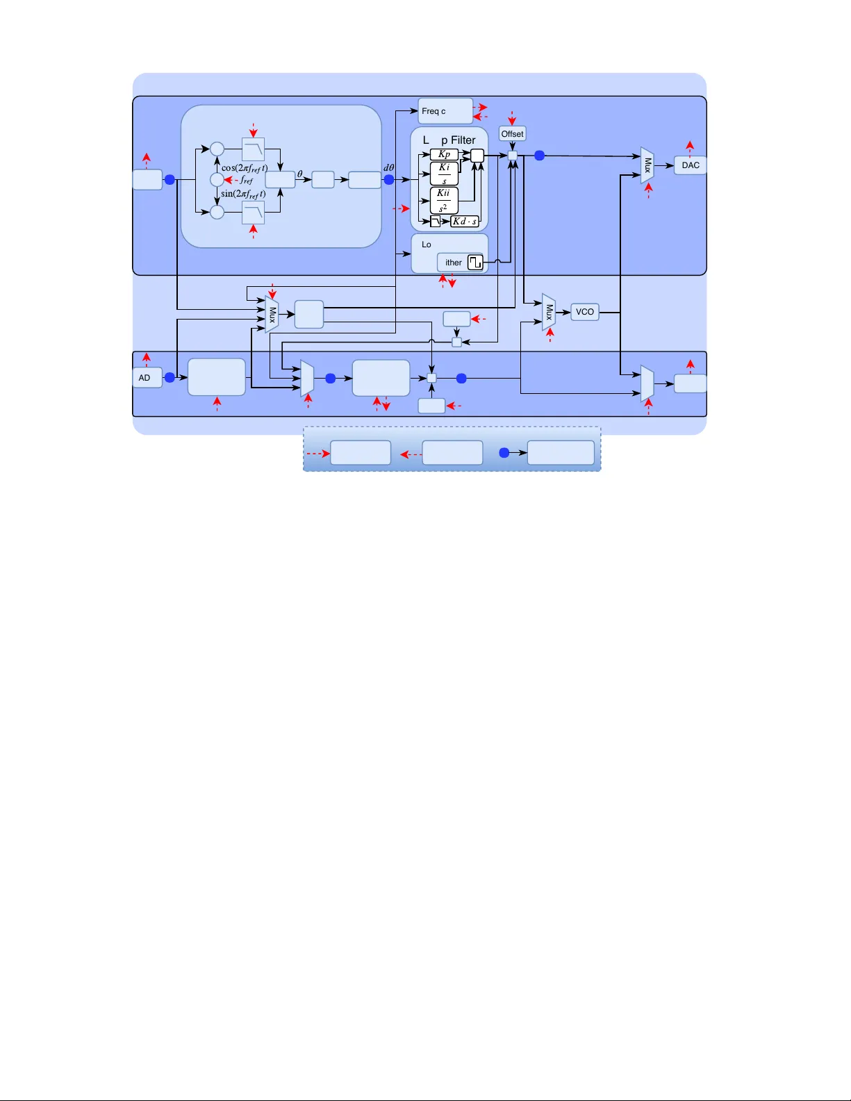
An op en and flexible digital phase-lo c k ed lo op for optical metrology This article may be downloaded for personal use only . Any other use requires prior permission of the author and AIP Publishing. This article appeared in Review of Scientific Instruments 89, 093103 (2018) and may b e found at https://doi.org/10.1063/1.5039344 An op en and flexible digital phase-lo ck ed lo op fo r optical metrology Alex T ourigny-Plante, 1 Vincent Michaud-Belleau, 1 Nicolas Bourb eau H ´ eb ert, 1 Hugo Bergeron, 1 J ´ erˆ ome Genest, 1 , a) and Jean-Daniel Desch ˆ enes 1, 2 , b) 1) Centr e d‘optique, photonique et laser, Universit´ e L aval, Qu´ eb e c, QC, G1V 0A6, Canada 2) OctoSig Inc. Qu´ eb e c, Canada (Dated: 7 May 2018) This paper presen ts an op en and flexible digital phase lock lo op optimized for laser stabi- lization systems. It is implemen ted on a cheap and easily accessible FPGA-based digital electronics platform (Red Pita y a) running a customizable op en-source firmw are. A PC- based softw are interface allo ws con trolling the platform and optimizing the lo op parameters remotely . Several to ols are included to allo w measurement of quan tities of in terest smo othly and rapidly . T o demonstrate the platform’s capabilities, we built a fib er noise canceler ov er a 400 m fib er link. Noise cancellation was achiev ed ov er a 30 kHz bandwidth, a v alue limited mainly by the delays introduced b y the actuator and by the round-trip propagation ov er the fib er link. W e measured a total latency of 565 ns for the platform itself, limiting the theoretically ac hiev able control bandwidth to approximately 225 kHz. I. INTRODUCTION The use of digital electronics for optical systems and serv o lo ops is steadily gaining traction. F or example, digital phase meters 1 are used for gravitational wa ves detection 2–4 and digital phase-lo c k ed lo ops (DPLL) are deplo y ed for frequency com b lo cking 5,6 , Doppler cancel- lation in optical links 7–9 as w ell as optical time transfer 10 . This is due to sev eral adv antages of digital serv os such as soft w are reconfigurability , easy replication and the p os- sibilit y of ha ving adv anced diagnostic to ols 11 . In applications where low latency and large control bandwidth are imp ortant, field programmable gate ar- ra ys (FPGAs) app ear as platforms of choice thanks to their intrinsically parallel and reconfigurable architec- ture. Digital platform can also directly track the phase of the signal instead of its trigonometric represen tation, whic h causes am biguit y (i.e. cos 2 π = cos 4 π ). This wider trac king p ossibilit y allo ws using to ols to c haracter- ize the external system ev en when the free running sys- tem has phase noise greater than the linear region of the trigonometric function. How ev er, the complexities asso- ciated with designing and programming a mixed mo de electronics board where fast analog signals are digitized, pro cessed and re-generated in real time are how ev er usu- ally not in a typical laser me trologist’s to ol chest and the price of FPGA-based systems is often prohibitive. These constitute imp ortant en try barriers preven ting de- plo ymen t of p ow erful digital platforms to a wider set of optical applications. In this pap er, we presen t an op en DPLL platform built around the Red Pita y a, a cheap and easily accessible FPGA-based b oard 12 . The Red Pitay a can be purchased for a few hundred dollars, a fraction of what commer- cial analog lo ck b oxes cost. The platform described here a) Electronic mail: jgenest@gel.ulav al.ca b) Electronic mail: o ctosigconsulting@gmail.com consists of a firmw are installed on a Red Pitay a b oard as w ell as a Python-based PC graphical user in terface (GUI) that remotely connects to b oards in order to monitor and optimize the servo lo op p erformance. The firm w are and softw are are op en-source and can b e do wnloaded, along with the installation instructions and user guide, using the link in the references 13 . The soft ware should be cross-platform, but the installation instructions are only pro vided for Windo ws and MacOSX. This work is based on the open-source design presen ted in 5,14 no w ported and adapted to Red Pitay a b oards so that custom hardware is no longer required. An optional in ternal v oltage-con trolled oscillator (VCO) has also been added to facilitate the integration with common opti- cal comp onents, for example the acousto-optic mo dula- tor (A OM) used to frequency-shift an optical field in a fib er noise canceled link, as presen ted in section I I I. Al- though this platform is not limited to optical metrology , the tools describ ed in section II w ere optimized with that application in mind since the residual phase is not as im- p ortan t when dealing with muc h higher optical carrier frequencies (compared to RF signals) and since there is a stronger fo cus on lo w ering the cycle slip probabilit y . F or some applications, FPGA platforms can b e highly optimized to p erform a single task 7 while in other cases the goal is to offer as many digital instrumen ts as p ossible 15,16 . The platform presented here sits in be- t w een these tw o extremes. The goal is to provide laser scien tists with a straigh tforw ard access to a fast and flexi- ble DPLL. With the design complexit y tac kled on generic off-the-shelf commercial electronics, the replication cost of this system is very low and the DPLL can easily b e deplo y ed in a v ariety of optical applications. I I. FIRMW ARE ARCHITECTURE Red Pitay a boards are based on a Xilinx Zynq 7010 FPGA and are programmed using Viv ado 2015.4 with a mix of VHDL and V erilog. The b oard is equipp ed An op en and flexible digital phase-lo c k ed lo op for optical metrology 2 with tw o analog inputs and tw o analog outputs. The analog-to-digital and digital-to-analog conv erters (ADCs and DA Cs) ha v e a resolution of 14 bits (a 10 bit v ersion is also av ailable and is compatible with the DPLL described here) and are, by default, driven b y the same 125 MHz crystal that is clo c king the FPGA. The Red Pita y a’s in- puts are equipp ed with 50 MHz low-pass anti-aliasing filters 17 . Each board can th us pro vide tw o DPLL that can b e indep enden t or in terlink ed, as describ ed b elo w. Figure 1 shows the complete representation of the DPLL arc hitecture. F or each channel, the signal is ac- quired by an ADC. Its in-phase and quadrature (I/Q) comp onen ts are extracted via multiplication with the sine and the cosine of a reference signal whose frequency is de- fined by a rational fraction on 48 bits chosen by the user ( f ref = k/ 2 48 · f clk ) 18 . The I/Q signals are lo w-pass fil- tered digitally with a selectable bandwidth (3.75 MHz, 15.5 MHz or 31 MHz). An arctangent op eration is then used to extract the phase error and a difference of succes- siv e phase measurements (numerical deriv ativ e) is used to alleviate dynamic range issues with the numerical repre- sen tations in the FPGA since a phase ramp is unbounded while its deriv ative is bounded. The mo dulo [ − π , π ] oper- ator handles the wrapping of the phase slope produced by the arctan. The phase incremen t signal is the input of the lo op filter implemen ting a prop ortional/integral/double in tegral/deriv ative (PII 2 D) con troller 19 . The double in- tegrator term ensures a null static error even with the nu- merical phase deriv ativ e previously made. The resources usage for this platform is presen ted in table I. Resource Used Av ailable Lo ok-up table (LUT) 8449 17600 LUT RAM 370 6000 Flip-Flops (FF) 12505 35200 Blo c k RAM (BRAM) 53.50 60 DSP Slices 69 80 Global clo ck buffer (BUFG) 9 32 Mixed-mo de clo ck manager 1 2 (MMCM) Phase-lo c k ed lo op (PLL) 2 2 T ABLE I. Red Pitay a resources usage. The ADC chips used in the Red Pitay a hav e a nom- inal time -domain signal to noise ratio (SNR t ) of 73 dB (compared to a theoretical 86 dB for 14 bits) but the o v erall p erformance of the Red Pita y a system with 14 bits ADCs is a SNR t of 63 dB, corresp onding to 10.2 effective num ber of bits (ENOB). The time domain SNR t is equiv alent to the sp ectral SNR f in a band- width from 0 to f s /2. The sp ectral SNR f is the SNR seen with a bandwidth of B W Hz and is describ ed by SNR f = SNR t + 10 log 10 ( f s 2 B W ). F or instance, when op- erating at a 125 MS/s sampling rate, this pro vides a SNR o v er 72 dB in a 7 . 5 MHz bandwidth, whic h is w ell ab ov e the SNR usually obtained in b eats inv olving frequency com bs 20 . The output of the lo op filter is enco ded in to 16 bits. When the VCO is not connected, the 14 most signifi- can t bits (MSBs) are directly sent to the 14-bit DA C and mapp ed to a voltage betw een − 1 and +1 V at the SMA outputs. When the V CO is connected, the 16 bits are instead used to represen t a frequency betw een 0 and the Nyquist frequency ( f s / 2). The 16 bits are mapp ed suc h that 0 = 0 Hz and 2 16 − 1 = 62 . 5 MHz, corresp ond- ing to a gain of 31.25 MHz/V. Adding an offset at the output via the control softw are allows adjusting the qui- escen t frequency . The desired tone is generated using an in ternal direct digital syn thesis (DDS) and this signal is sen t to the DA C with a user selected amplitude and DC offset. The addition of a dither signal allows for an easy char- acterization of the system to b e con trolled. The dither mo dule generates a square w a v e with a selectable ampli- tude and frequency . This signal is added just after the lo op filter’s output and th us it constantly excites the sys- tem b eing con trolled. Lo ck-in detection 21 of this square w a v e at the input side of the mo dule allo ws measuring the controlled system’s gain in Hz/V, including its sign. This gives the op erator a constan tly up dated kno wledge of the lo op’s sign and is useful for p erforming loop tuning in relev ant units. The lo op filter parameters are user selectable in the GUI. The prop ortional gain ( k p ) is defined in dB rela- tiv e to the open-lo op DC gain of the system ( k c ), suc h that the linear gain is K p = 10 k p / 20 /k c . The in tegrator, double integrator and deriv ative are sp ecified by their crosso v er frequencies, f i , f ii and f d , resp ectively . The in- tegrator and the differentiator crossov er frequencies can b e defined either b y the 0 dB crossov er or by the k p crosso v er. The double integrator crossov er frequency is defined b y the in tersection with the in tegrator. Finally , a first-order filter implemen ts a roll-off frequency for the differen tiator ( f d f ). T able II presents the equations link- ing the lo op filter gain v alues ( K p , K i , K ii and K d ) to the user settings and the system parameters. A factor 2 π /f s tak es into account the fact that the n umerical deriv ativ e and integrators are relative to the sampling frequency ( f s ). When including the previous numerical deriv ative, the PI I 2 D controller in fact acts as a PIDD 2 . F or most systems b eing con trolled, the double differentiator term w ould not b e used and is normally turned off. How ev er, this can b e useful for example with a system containing t w o dominan ts first order roll-offs. V ariable Relative to 0 dB Relativ e to K p K p 10 k p / 20 1 k c K i 1 k c f i 2 π f s K p f i 2 π f s K ii K i f ii 2 π f s K d 1 k c 1 f d f s 2 π K p 1 f d f s 2 π D filter f d f 2 π f s T ABLE I I. Lo op filter gain equations. k c : system op en-lo op DC gain, f s : sampling frequency (125 MHz) . Diagnostic information can b e sent from the Red Pita y a to the PC-based control soft w are. The spectrum An op en and flexible digital phase-lo c k ed lo op for optical metrology 3 FPGA Legend d θ ADC Differential Phase Extraction Freq Counter Loop Filter Dither Mux Offset Mux ADC DAC VNA Differential Phase Extraction Arctan Modulo Diff θ I Q c o s ( 2 π t ) f r e f s in ( 2 π t ) f r e f f r e f Loop Filter Mux K p K i s K d ⋅ s K i i s 2 Offset Mux Mux DAC Lock-in module Dither VCO Freq counter Offset Communication from computer Communication to computer Oscilloscope to computer x x ~ + + + + FIG. 1. Complete blo ck diagram of the DPLL platform’s firmw are. Red arro ws represent the comm unication with the PC soft ware and blue dots represen t the test points at which signals can be sho wn in the PC softw are. The second channel is a duplicate of the first. ADC: Analog-to-digital con v erter, MUX: Multiplexer, VNA: V ector net work analyzer, VCO: V oltage- con trolled oscillator, DA C: Digital-to-analog conv erter. of all signals represented by a blue dot in figure 1 can be computed and display ed in real-time in the GUI; temp o- ral represen tations are also a v ailable. Baseband comp o- nen ts are represen ted in a con v en tional I/Q diagram for analysis at-a-glance while the phase and frequency noise p o w er sp ectral density (PSD) and total integrated phase noise are also con tin uously up dated. A zero dead-time frequency counter with a 1 second gate time allows mon- itoring and logging the lo c k’s long-term p erformance. A vector netw ork analyzer (VNA) integrated to the platform mak es the measuremen t of the system’s trans- fer function p ossible. Measuremen ts of the magnitude and phase are display ed in the PC-based softw are, allow- ing for an easy tuning of the controllers, and data can also b e exp orted for further analysis. When the internal V CO is used, its con tribution is included in the measured VNA’s transfer function. Thus, the measured frequency resp onse includes the contributions of the VCO, external setup and delays associated to the FPGA pro cessing with an input calibrated in Hz and an output calibrated in V. Soft w are controllable m ultiplexers allo w using the FPGA in three different con trol scenarios. First, the platform can op erate as t w o indep endent con trol lo ops eac h using their own ADC, demodulation block, lo op fil- ter and DA C. F or instance, one c hannel can be used to lo c k the carrier offset of a frequency com b and the other to lo ck one com b to oth to a reference laser, as done by Sinclair et al. 5 . A single Red Pitay a box can therefore fully reference a frequency comb. The only cav eat in this mo de is that only one VCO is av ailable and thus only one of the c hannel can use it. The second con trol scenario consists in having t w o par- allel lo ops using only one input. In that c ase, b oth chan- nels share the same ADC and demo dulation blo ck. After the differential phase extraction, the error signal how- ev er pro ceeds independently in the tw o distinct loop fil- ters with p otentially different transfer functions. This allo ws controlling tw o differen t actuators acting on the same system with differen t frequency resp onses. F or in- stance, one might w an t to close a lo op with a fast but short-strok ed piezo electric actuator on one side and, on the other side, a slo w er actuator with longer strok e 5 . In the third scenario, it is p ossible to seed the output of the first channel to the input of the second filter lo op. This configuration can b e used to maintain the output of the first c hannel around a certain setpoint by controlling another actuator with the second channel. This metho d is used to sta y in the activ e range of a fast actuator b y relying on a slo w actuator. F or example, Sinclair et al. used a slo w piezo electric actuator to sta y within the dy- namic range of a fast piezo electric actuator 5 . The whole system latency is τ = 407 ns (565 ns with the VCO), which limits the noise rejection bandwidth to approximately 1 / 8 τ = 300 kHz (225 kHz with the V CO). This estimation of the maximum bandwidth as- sumes that a lo op is closed around a first order system with π /4 of phase margin. Of the 407 ns latency , 207 ns comes from the demo dulation pro cess and the remaining comes from the lo op-filter, ADC and D A C. The comm unication b etw een the FPGA and the com- An op en and flexible digital phase-lo c k ed lo op for optical metrology 4 puter is made via a TCP connection con trolled by the Python softw are. A notable feature of this up dated ver- sion is the capabilit y to disconnect the PC con trol soft- w are, allo wing locks to operate in a standalone mode, and reconnect when supervision, data acquisition or modifi- cations of the parameters are needed. I I I. FIBER NOISE CANCELER A fiber noise canceler (or Doppler canceler link) is a commonly used tool in optical frequency metrology 7–9,22 . Here, we used a Doppler cancellation link to v alidate the op eration of the DPLL on the Red Pitay a platform and to demonstrate new features, such as the in tegrated VCO. Figure 2 shows the experimental setup used to achiev e the stable transfer of a laser frequency to a remote lo ca- tion o v er a fib er link. In the c hosen configuration, part of the laser light reaching the remote site is reflected to the transmission site. This round-trip light th us experiences, at low frequencies, double the delay and double the phase fluctuations imp osed by the link on the transmitted sig- nal, as sho wn b y Williams et al. 22 . Comp ensation for the measured fluctuations is done using an A OM fed b y the Red Pita y a’s new feature, the V CO, whic h is controlled b y the DPLL. Local site FPGA Remote site Laser AOM (+~27MHz) 98/2 Coupler 90/10 Coupler 50/50 Coupler Output 400m Delay PC ADC Differential Phase Extraction Loop Filter VCO DAC Amplifier + ν 0 f r e f 2 Balanced photodetector ν 0 ν + f r e f 0 FIG. 2. Exp erimen tal setup for the fib er noise canceled link. Solid lines represent optical fib ers and dashed lines represen t electrical interconnects. In our exp erimen tation, f ref = 54 M H z . PC: p olarization controller, AOM: acousto- optic mo dulator A t the local site, the b eat note b etw een the lo cal os- cillator (LO) and the reflected signal is fed to the DPLL. Its phase con tains information about the fluctuations in the link’s optical length that ha v e to b e corrected. As the nominal frequency of the AOM used here is 27 MHz, I/Q demo dulation is performed with a reference frequency of 54 MHz in order to extract the phase error. The out- put offset is adjusted to set the quiescent frequency at 27 MHz. In order to c haracterize the A OM used in the exp er- imen t, we measured its transfer function with a differ- en t setup in whic h a beat b etw een the input and output signals of the AOM was acquired. The resulting curv e, displa y ed in blue in figure 3, represents the transfer func- 10 6 10 7 10 8 Gain [Hz/V] 10 3 10 4 10 5 10 6 Frequency [Hz] -40 -30 -20 -10 0 Phase [rad] H AOM+VCO H sys measured H sys predicted FIG. 3. T ransfer function of the AOM-V CO combination (blue) and the complete Doppler cancellation link (orange), as measured by the platform’s VNA. The A OM-V CO combina- tion transfer function (blue) is use to determine the complete theoretical transfer function (red). The complete experimen- tal transfer function (orange) matches the theoretical one. tion of the combination of A OM and VCO. The A OM’s latency , 1 . 5 µs , was computed from the transfer function based on the appro ximation that it mainly acts as a dela y in the frequency range of in terest. Therefore, this dela y is larger than the in trinsic FPGA’s latency and will alw a ys lead to a significan tly lo w er noise rejection bandwidth. Multiplying the AOM+V CO transfer function b y the fib er optic dela y and the cosine square shap e of the dou- ble pass through the AOM leads to an excellent superp o- sition with the transfer function measured by the VNA for the system sho wn in figure 2. The first zero of the cosine at 0 . 125 MHz is determined b y the fib er link dif- feren tial dela y whic h is here 2 . 0 µs (400 m). With a total effectiv e dela y of 4 . 0 µs (optical fib er 2 . 0 µs , A OM 1 . 5 µs and FPGA 0 . 5 µs ), the maximum achiev able closed-lo op bandwidth in this demonstration is th us 31 . 25 kHz. When the lo ck is active, the VNA can still b e used to output perturbations in the system in order to c haracter- ize the closed-loop noise rejection, as shown i n figure 4a). This figure displays the theoretical gain for uncorrelated distributed fiber noise at the remote link output, whic h is one of the noise our lock aims to cancel. T o v alidate the mo del used to determine this transfer function, the ex- p erimen tal and predicted transfer functions for the V CO noise at the local site are sho wn. This experimental curv e w as easier to obtain since it could b e measured without the addition of external comp onents as the VCO w as the only actuator. How ever, one could use a differen t chan- nel to control an actuator to introduce disturbance at another p oin t in the system. A visual represen tation of the obtained PSD is giv en in figure 4b). This figure sho ws b oth closed-loop (purple curv e) and op en-lo op (orange curve) PSDs at the remote site. In this figure, it is p ossible to observe that the sys- tem noise rejection bandwidth is around 30 kHz, which fits with the exp ected maxim um bandwidth. The PSDs presen ted here are the result of a b eat b etw een the laser and the remote signal. Therefore, the display ed interfer- ometric phase noise is necessarily lo w er than the laser’s An op en and flexible digital phase-lo c k ed lo op for optical metrology 5 phase noise b elow 1/(4 τ ) 23 . W e can th us conclude that, after propagation in the Doppler-canceled link, the phase noise added by out-of-lo op fibers w ould be negligible with resp ect to laser phase noise. -100 -80 -60 -40 -20 0 20 Gain [dB] (a) kp = -9.0 dB f i = 1.5e3 Hz f ii = 3.0e3 Hz f d = ∞ Hz Predicted fiber noise gain (remote) Predicted VCO noise gain (local) Measured VCO noise gain (local) 10 1 10 2 10 3 10 4 10 5 10 6 Frequency [Hz] 10 -12 10 -10 10 -8 10 -6 10 -4 10 -2 Phase noise PSD [rad 2 /Hz] 10 -8 10 -6 10 -4 10 -2 10 0 Phase [rad] (b) Open-loop, estimated laser contribution Open-loop, measured Closed-loop, predicted from open-loop Closed-loop measured Estimated out-of-loop noise Closed-loop integrated phase noise FIG. 4. a) Predicted closed-loop transfer functions for v arious noises and disturbances present in the system. The built-in VNA was used to measure the noise rejection transfer function for noise injected at the local end of the link (yello w). The re- mark able agreemen t with the prediction (orange) yields cred- ibilit y to other predictions based on the same set of estimated parameters. b) Comparison of the remote output phase noise PSD measured with an out-of-lo op oscilloscop e. The closed- lo op prediction curve (y ello w) is obtained by multiplying the op en-loop phase noise PSD (orange) b y the appropriate trans- fer functions, assuming that it is largely dominated by laser noise. A rough estimation of the out-of-lo op noise (green) w as p erformed by bypassing the 400 m delay to directly con- nect the AOM to the remote site. Obviously , this out-of-loop noise constitutes the main contribution to closed-lo op noise b elo w 1 kHz; since its lev el is low ered when we activ ate an an ti-vibration table, w e conclude that it is most likely due to residual building vibrations. The cumulativ e in tegrated phase noise (blue dots) is also shown. IV. CONCLUSION In summary , we hav e demonstrated the use of an op en-source DPLL platform b y p erforming an optical fre- quency transfer o v er a fiber noise canceled link. The tools a v ailable on this platform allow to simplify the analy- sis of the system by offering an on-b oard VNA to mea- sure transfer functions and by pro viding v arious real-time quan tities such as PSD, I/Q, sp ectrum, time signal, fre- quency error and lo op filter’s transfer function. The dif- feren t to ols and con trol scenarios allo w the use of this c heap and accessible platform for several optical applica- tions. Since this platform is open source, w e in vite ev- ery one to con tribute to its impro v emen t, for example b y minimizing the latency to increase the achiev able lo c king bandwidth. V. A CKNO WLEDGEMENTS The authors wan t to thank the supp ort from the Natural Sciences and Engineering Research Council of Canada(NSER C). 1 C. W ang and J. D. E. E.D. Burnham-F ay , Precision Engineering , 133 (2017). 2 D. Shaddo ck, B. W are, P . G. Halverson, R. E. Sp ero, and B. Klipstein, AIP Conference Pro ceedings 873 , 654 (2006), http://aip.scitation.org/doi/pdf/10.1063/1.2405113. 3 T. G. McRae, S. Ngo, D. A. Shaddo ck, M. T. L. Hsu, and M. B. Gray , Opt. Lett. 39 , 1752 (2014), http://ol.osa.org/abstract.cfm?URI=ol-39-7-1752. 4 K.-S. Isleif, O. Gerb erding, S. K¨ ohlenbeck, A. Sutton, B. Sheard, S. Goßler, D. Shaddo ck, G. Heinzel, and K. Danzmann, Opt. Express 22 , 24689 (2014). 5 L. C. Sinclair, J.-D. Desc henes, L. Sonderhouse, W. C. Swann, I. H. Khader, E. Baumann, N. R. Newbury , and I. Co d- dington, Review of Scien tific Instruments 86 , 081301 (2015), http://dx.doi.org/10.1063/1.4928163. 6 M. Lezius, T. Wilken, C. Deutsch, M. Giunta, O. Mandel, A. Thaller, V. Schk olnik, M. Schiemangk, A. Dinkelak er, A. Ko- hfeldt, A. Wich t, M. Krutzik, A. Peters, O. Hellmig, H. Dunc k er, K. Sengsto ck, P . Windpassinger, K. Lampmann, T. H ¨ ulsing, T. W. H¨ ansch, and R. Holzwarth, Optica 3 , 1381 (2016). 7 A. C. C. Olay a, S. Micalizio, M. Ortolano, C. E. Calosso, E. Ru- biola, and J. M. F riedt, “Digital electronics based on red pitay a platform for coherent fib er links,” (2016). 8 S. Droste, F. Ozimek, T. Udem, K. Predehl, T. W. H¨ ansch, H. Schnatz, G. Grosche, and R. Holzw arth, Phys. Rev. Lett. 111 , 110801 (2013). 9 C. E. Calosso, C. Cliv ati, and S. Micalizio, IEEE T ransactions on Ultrasonics, F erroelectrics, and F requency Control 63 , 646 (2016). 10 J.-D. Desch ˆ enes, L. C. Sinclair, F. R. Giorgetta, W. C. Swann, E. Baumann, H. Bergeron, M. Cermak, I. Co dding- ton, and N. R. Newbury , Phys. Rev. X 6 , 021016 (2016), https://link.aps.org/doi/10.1103/Ph ysRevX.6.021016. 11 C. E. Calosso, E. Bertacco, D. Calonico, C. Cliv ati, G. A. Costanzo, M. F rittelli, F. Levi, A. Mura, and A. Go done, Opt. Lett. 39 , 1177 (2014). 12 Instrumentation T echnologies LLC, “Red Pitay a,” https:// redpitaya.com/about- us/ (). 13 Jean-Daniel Deschenes, “Digital PLL co de base,” https:// github.com/jddes/Frequency- comb- DPLL . 14 J.-D. Deschenes, L. Sinclair, N. R. Newbury , and I. Co ddington, “Fpga-based digital con trol b ox for phase stabilization of a frequency comb (NIST version),” https://www.nist.gov/services- resources/software/ fpga- based- digital- control- box- phase- stabilization- frequency-comb. 15 Liquid Instruments, “Moku:Lab,” http://www. liquidinstruments.com/ . 16 L. Neuhaus, R. Metzdorff, S. Chua, T. Jacqmin, T. Briant, A. Heidmann, P . F. Cohadon, and S. Delglise, “Pyrpl (python red pitaya lockbox) x2014; an op en-source software pack age for fpga-controlled quantum optics exp eriments,” (2017). 17 Instrumentation T echnologies LLC, “Red Pitay a do cumenta- tion,” http://redpitaya.readthedocs.io/en/latest/ (). An op en and flexible digital phase-lo c k ed lo op for optical metrology 6 18 J. A. W ebb, “Digital quadrature demo dulator,” (1978), uS Paten t 4,090,145. 19 K. H. Ang, G. Chong, and Y. Li, IEEE transactions on control systems technology 13 , 559 (2005). 20 J.-D. Desch ˆ enes and J. Genest, Opt. Express 23 , 9295 (2015). 21 J. H. Scofield, American Journal of Physics 62 , 129 (1994), https://doi.org/10.1119/1.17629. 22 P . A. Williams, W. C. Swann, and N. R. New- bury , J. Opt. So c. Am. B 25 , 1284 (2008), http://josab.osa.org/abstract.cfm?URI=josab-25-8-1284. 23 V. Michaud-Belleau, H. Bergeron, P . S. Light, N. B. Hb ert, J. D. Deschnes, A. N. Luiten, and J. Genest, Metrologia 53 , 1154 (2016).
Original Paper
Loading high-quality paper...
Comments & Academic Discussion
Loading comments...
Leave a Comment