FPGA-based Multi-Chip Module for High-Performance Computing
Current integration, architectural design and manufacturing technologies are not suited for the computing density and power efficiency requested by Exascale computing. New approaches in hardware architecture are thus needed to overcome the technological barriers preventing the transition to the Exascale era. In that scope, we report successful fabrication of first ExaNoDe’s MCM prototypes dedicated to Exascale computing applications. Each MCM was composed of 2 Xilinx Zynq Ultrascale+ MPSoC, assembled on advanced 68.5 mm x 55 mm laminate substrates specifically designed and fabricated for the project. Acoustic microscopy, x-ray, cross-section and Thermo-Moire investigations revealed no voids, shorts, delamination, cracks or warpage issues. Two MCMs were mounted on a daughter board by FORTH for testing purposes. The DDR memories on the 4 SODIMMs of the daughter board were successfully tested by running extensive Xilinx memory tests with clock frequencies of 1866 MHz and 2133 MHz. All 4 FPGAs were programmed with the Xilinx integrated bit error ratio test (IBERT) tailored for this board for links testing. All intra-board high-speed links between all FPGAs were stable at 10 Gbps, even under the more demanding 31-bit PRBS (Pseudorandom Binary Sequence) tests.
💡 Research Summary
The paper presents the design, fabrication, and validation of the first prototype multi‑chip module (MCM) developed under the European H2020 ExaNoDe project, aimed at enabling exascale computing. Current supercomputers operate at petascale performance, which is insufficient for emerging scientific challenges such as computational biology, climate modeling, and energy research. To bridge the gap to exascale (10¹⁸ floating‑point operations per second), new hardware architectures that combine advanced packaging, three‑dimensional (3D) integration, and heterogeneous integration are required.
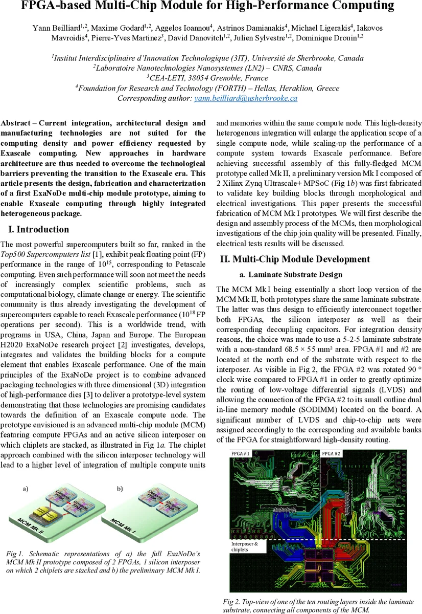
The prototype, designated Mk I, consists of two Xilinx Zynq UltraScale+ MPSoC devices mounted on a custom 68.5 mm × 55 mm laminate substrate. The substrate follows a 5‑2‑5 stack configuration and incorporates routing for low‑voltage differential signaling (LVDS), power distribution, and decoupling capacitors. Notably, FPGA #2 is rotated 90° relative to FPGA #1 to optimize LVDS routing and reduce trace lengths to the on‑board SODIMM memory sockets. The laminate was fabricated by Kyocera, and the assembly process employed a flux‑assisted C4 ball‑grid‑array (BGA) soldering technique followed by a copper‑under‑fill (CUF) encapsulation to mitigate thermal‑expansion mismatches and prevent delamination. A 1 mm pitch BGA with 600 µm wide solder balls was formed on the backside, and a 1 mm thick Cu/Ni lid served as a thermal interface material.
Morphological investigations—including scanning acoustic microscopy, X‑ray imaging, cross‑sectional microscopy, and Thermo‑Moiré analysis—demonstrated flawless assembly. No voids, non‑wetting, shorts, or cracks were observed in the C4 connections, and the maximum measured warpage was only 13.1 µm, well below the JEITA recommendation of 220 µm for 1 mm pitch BGA packages.
Electrical testing was performed after mounting the two MCMs on daughter boards (DB) supplied by the Foundation for Research and Technology (FORTH). Each DB incorporated a Minifeeder carrier providing ten SFP+ transceivers, a Gigabit Ethernet port, UARTs, and general‑purpose I/Os. The four DDR‑SODIMM modules on the DB were exercised with Xilinx memory test patterns at 1866 MHz and 2133 MHz, confirming stable operation. JTAG connectivity allowed programming of all four FPGAs, after which the integrated Xilinx IBERT (Integrated Bit Error Ratio Test) suite was used to evaluate high‑speed serial links. All intra‑board links between the four FPGAs remained error‑free at 10 Gbps, even under the more demanding 31‑bit PRBS traffic, indicating robust signal integrity and successful high‑speed routing.
The authors conclude that the successful assembly, card‑attach, and functional verification of the Mk I prototype demonstrate the feasibility of high‑density, energy‑efficient FPGA‑based MCMs for exascale applications. The next development phase (Mk II) will incorporate an active silicon interposer with two stacked chiplets, further increasing integration density and reducing interconnect latency. By validating both the mechanical reliability and the electrical performance of the prototype, this work provides a solid foundation for future 3D‑packaged compute nodes that can meet the demanding power‑efficiency and performance targets of the exascale era.
Comments & Academic Discussion
Loading comments...
Leave a Comment