A Behavioral Compact Model of 3D NAND Flash Memory
We present a behavioral compact model of 3D NAND flash memory for integrated circuits and system-level applications. This model is easy to implement, computationally efficient, fast, accurate and effectively accounts for the different parasitic capacitance coupling effects applicable to the 3D geometry of the vertical channel Macaroni body charge-trap flash memory. The model parameter extraction methodology is simple and can be extended to reproduce the electrical behavior of different 3D NAND flash memory architectures (with different page size, dimension, or number of stacked layers). We believe that the developed compact model would equip the circuit designers and system architects with an effective tool for design-exploration of 3D NAND flash memory devices for diverse unconventional analog applications.
💡 Research Summary
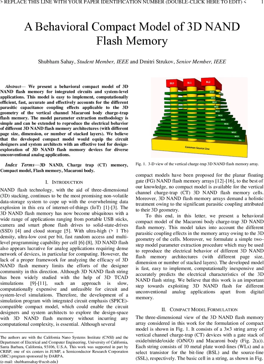
The paper presents a behavioral compact model for vertical‑channel, charge‑trap (CT) 3D NAND flash memory, targeting integrated‑circuit and system‑level design exploration. Recognizing that conventional 3D TCAD simulations are computationally intensive and unsuitable for large‑scale circuit analysis, the authors develop a SPICE‑compatible model that captures the unique three‑dimensional parasitic coupling inherent to the “macaroni‑body” architecture. The model represents each memory cell as a polysilicon gate‑all‑around nanowire FET (GAA‑NWFET) whose threshold voltage shift due to program/erase pulses is emulated by a voltage‑controlled voltage source (VCVS). Crucially, four distinct capacitances—horizontal (C_H), vertical (C_V), diagonal (C_D), and side (C_S)—are introduced to model coupling between adjacent cells in the same word line, between cells stacked along a string, and between diagonal or neighboring strings, respectively.
Parameter extraction follows a two‑step methodology. First, mixed‑mode Sentaurus TCAD simulations of a 3 × 3 × 3 array are used to obtain the geometry‑dependent coupling capacitances via an inverted nodal admittance matrix. The extracted values show that C_V dominates due to metal word‑line plates, while C_D is negligible for the considered cell morphology. In the second step, the basic cell is modeled with the BSIM‑CMG 110.0.0 compact model (cylindrical geometry). Because experimental data for cells at different string positions are unavailable, the authors calibrate the BSIM‑CMG parameters against TCAD‑generated single‑word‑line (single‑WL) I‑V curves for the top (WL0) and bottom (WL9) cells. The calibration includes adjusting channel resistance, mobility, and threshold voltage to reproduce the TCAD results, which themselves have been validated against published string‑current measurements.
The resulting compact model reproduces the multi‑WL string current characteristics with high fidelity while offering simulation speeds orders of magnitude faster than full 3D TCAD. The authors demonstrate that the model can be extended to other 3D NAND configurations—different page sizes, array dimensions, or numbers of stacked word lines—by repeating the same extraction steps. They also discuss how program/erase behavior can be incorporated by tuning the VCVS parameters.
In conclusion, the work delivers a fast, accurate, and easily implementable behavioral model that accounts for the full three‑dimensional electrostatic coupling of 3D NAND flash arrays. This enables circuit designers and system architects to explore unconventional analog applications such as in‑memory computing, neuromorphic accelerators, and other emerging paradigms without incurring the prohibitive computational cost of full TCAD. Future directions include incorporating grain‑boundary‑induced variability, validating against larger‑scale experimental arrays, and refining the model for higher‑stacked word‑line strings.
Comments & Academic Discussion
Loading comments...
Leave a Comment