Digital Neuron: A Hardware Inference Accelerator for Convolutional Deep Neural Networks
We propose a Digital Neuron, a hardware inference accelerator for convolutional deep neural networks with integer inputs and integer weights for embedded systems. The main idea to reduce circuit area and power consumption is manipulating dot products…
Authors: Hyunbin Park, Dohyun Kim, Shiho Kim
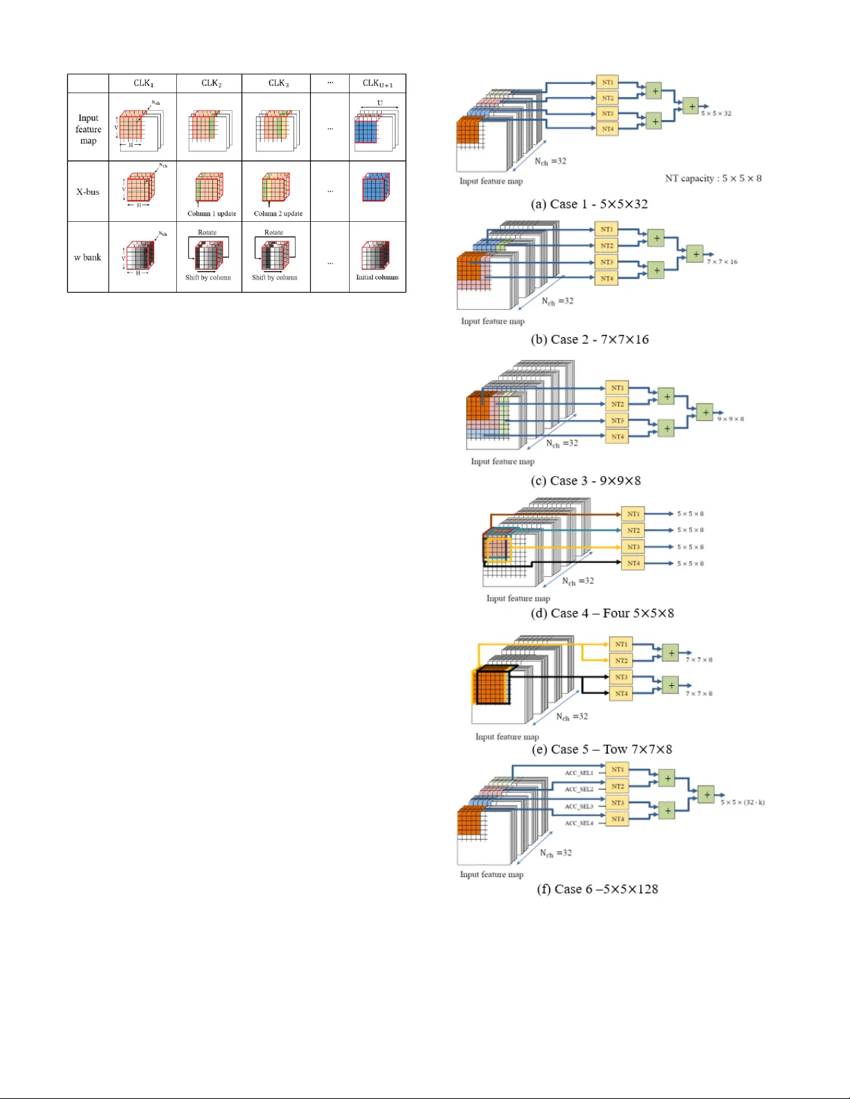
1 Abstract — We pro pose a Digita l Neuron, a hardw are inference accelerator for convolutional deep neural networks w ith integer inputs and integer weig hts for embedded systems. The main idea behind this concept is to reduce t he circuit area an d power consumption by m anipulating the d ot products between the input feature and w eight vectors using barrel shifters and parallel adders. The reduced area allows m ore computational engines to be mounted on an inference accelerator, resulting in a hi gh throughput compared to that of other hardware accelerators. We transformed the multiplication of two 8 -bit integers into 3-partial sub-integers and verified it does not cause a significant loss in the inference accuracy c ompared to that in the 32 -bit floating point calculation. The proposed digital neuron c an perform 8 00 Multiply-and-Accumulation (M AC) operations in one clock for convolution as w ell as full-connection. This paper provides a scheme that reuses the input, weight, and o utput of all layers to reduce DRAM access . In addition, it pr oposes a co nfigurable architecture t hat can enable the inference of adaptable feature of convolutional neural networks. The throughput of t he digital neuron in terms of watts is 754.7 GMACs/W. I. I NTRODUCTION EEP learning has revol utionized the computer industr y over the last decades, p ushing the accuracy of image recognition beyond that of humans [1]. However, the computational effort of current neural networ ks depends on the power-hungr y parallel floating-point pr ocessors or General- Purpose computing o n Grap hics P rocessing Units ( GP -GPUs) . Recent developments in hard ware accelerators have significantly reduced energy consumptio n; ho wever, devices with e mbedded s ystems suc h as d rones, s mart ro bots, and autonomous vehicle s are still facing hard limita tions caused by power budget for ultralo w power applications. Several studies have ado pted a strategy for training u sing a desktop or server and inference using a hardware accelerator i n embedded devices [ 2]-[4 ]. To utilize the hard ware inference accelerator in an embedded s ystem, the neural weights in the single- or half-precision Float ing P oint for mat (FP32 or FP16) should be converted in to integers. The key is sues w ith hard ware acce lerators in em bedded “ This rese arch was su pported by the MSIT(Ministry of Science a nd I CT), Korea, under the I CT Consilience C reative program(II TP- 201 8-2017-0- 01015) supervise d by the IITP(I nstitute for Information & communications Technolo gy Pro motion), by Institute for Information & communica tions Technolo gy Promotion(IITP) grant funded by t he Korea government(MSI P) systems ar e accuracy lo ss, po wer con sumption, circuit area, an d throughput. To im prove the thr oughput and power consumptio n, several studies [5]-[8] ha ve r educed the bit-width o f the i nput and w eight compared to those in th e conventional FP32 format . The reduction in the bit-wid th decreases circuit area of computational engine, which therefore allows m ore computational engines to be mounted in a li mited ar ea. Therefore, it can increase the throu ghput. Gysel [5 ] suggest ed quantizing inp uts a nd weights into 8 -bits in forward propagation, resulting in accuracy loss of less than 1 % in LeNet-5 [9] , AlexNet [ 10 ], and Sq ueezeNet [ 11 ]. (No.2017-0-00244, HMD Facial Expression Recognition Sensor and Cyber- interaction I nterface Technol ogy) The au thors are with the School of Integrated Technology , Yonsei University, Seoul, Korea (e-mail: bin9000@yonsei.ac.kr; kimdh5032@nave r.com; shiho@y onsei.ac.kr). Digital Neuron: A Hardware Inference Accelerator for Convolutional Deep Neural Networks Hyunbin Park, Do hy un Kim, and Shiho Kim D TABLE I Simulated infer ence accuracy of MNIST handwritten num ber in Le Net - 5 [9] according to resolution of w eights, w here pre-trained we ights in the networ k with FP32 are qua ntized to integer weights. Infere nce accuracy 32 -bit flo ating-point repre sentation 99.10 % 8-bit intege r weights 99.10 % 5-bit intege r weights 98. 95 % Proposed 5-bit integ er we ights with two partial s ub-integer s 98. 92 % Proposed 8-bit integ er we ights with three partial sub-integer s 99.10 % Fig. 1 Represe ntation of integers from 0 to 128 partitioned into 2 or 3 partial sub-intege rs. 2 BinaryConnect (BC) [ 12 ] reduced the b it-width of w eights ev en further to 1-bit. Ho wever, limiting bit-width of weights to 1-bit degrades the ImageNet T op-1 inference ac curacy by 21 .2 % in AlexNet [ 10 ]. T herefore, it is important to design hardware accelerators with an optimum bit- width to achieve an acc uracy within the target ran ge. We si mulated inference accuracy of an MNIST handwritten number in LeNet-5 [9] according to the b it-width of the weights in Table I, where pre-trained weights in the network with FP 32 were quantized to integer weights. Q uantization into 8-bit integer weights does not degrad e the in ference acc urac y compared to that in the cas e with FP3 2. In addition, the accuracy degradation in t he case of the net work with 5 -bit integer weights is negligible. Artificial neurons in the Integrate and Fire m odel [ 13 ] perform a convolution by cal culating the inner prod uct o f the input and weight vect ors: (1) where X , w , b, F , and Out ar e an input vector, weight vector , bias, activation function, and o utput, respectively. If the multiplications required for the inner prod uct are i mplemented via arith metic shift and addition, a multiplier circuit that is mo re simple t han that using the bo oth multiplier can be designed . Booth multiplication with an 8-bit weight p roduces five partial products includin g the ad dition of 1 for the 2’s co mplement [ 14 ] . However, neural networ ks do not require exact algebraic calculations. T herefore, w e quantized the weight into the su m of a lim ited n umber of s, which we call t he ‘partial sub integer, ’ e.g. , with t wo sub -par tial integers. Fig. 1 sh ows a representation of 8-bit integers partitioned in to 2 or 3 partial sub-i ntegers, which is expressed by (2) where N can be 2 or 3. It allows a multiplier to be im plemented by only two- or th ree-barr el shift circuits. T he maximum error s caused by the quantization by li miting the partial sub -integers into t wo a nd three are ap proximatel y 9 % and 2 %, respecti vely . Despite the calculation error in multiplication, the degradation caused by this qu antization is negligible, as shown in Table I. T his study employs the strategy of limiting partial sub-integers to increa se throughput and red uce po wer consumption . It has b een found that DRAM ac cess co nsumes 200 times more po wer than regi ster access [15] . Inference accelerato rs with a spatial architecture, reported in [1 6]-[ 18 ], allow a computational engine to d eliver the inp ut, weight, and t he Partial sum of the o utput (Psum) to an adjacent computatio nal engine. Such spatia l architectures reu se t he input, weight, and Psum, helping to reduce DRAM access. However, computation in the Full y-Connected (F C) la yer does not r equire inp ut and weight reuse; thus, the spatial architecture is str ucturally disadvantageous for co mputation in the FC la yer . In ad dition , the outputs of the la yers a re not reused in [ 16]-[18], as additional DRAM acce ss i s required for loading and stor ing outputs of layers. This paper proposes a dig ital neuron, a configurable in ference acceler ator for embedded systems. T he throughput is improved by red ucing the ci rcuit area o f t he computational engine. The pro posed digital neuron also fully utilizes computational engines with a massive parallel structure. In addition, a reuse sc heme for the layer o utputs is presented for reducing DRAM acce ss . II. R ELATED W ORKS This section reviews previous works that use multiplication with a s hift circuit to reduce the complexity of a co mputation engine. In addition, it r eviews prior arts of inferen ce accelerators with a spatial architecture and ho w they reuse data and perform FC computatio ns. A. Previo us works with shift -based multipliers Several hardware ac celerator s use the M ultiply a nd Accumulation (MAC) structure for computing the dot product [19]-[21]. The MAC structure multiplies the inp ut and weig ht with a binar y multiplier (e. g. boo th multiplier [14 ]) and accumulates t he multiplied va lue with a binary add er (e.g. Carry Look Ahead (CLA) ad der [ 22 ]) , as shown in Fig. 2 (a). A shift circuit has been adopted for arithmetic multiplication to reduce the circ uit area of a multiplier [23], [ 24] . UNPU, a hardware accelerator reported in [23], produces 16 partial products with 16 s ets of A ND g ate, binary adder, and 1-bit sh ift circuit, as shown in Fi g. 2 (b). The UNP U can support multiplication with weights of all bit -widths from 1-bit to 16- bits. T he B IT FUSION sche me [24] decomposes, for exa mple, 4-bit multiplication into four 2 -bit multiplicatio ns, as shown in Fig. 2 (c). By ad justing the combinatio ns o f the deco mposed multiplications, this system also can support f lexible bit-widths of the weights. The proposed digital neuron for reducing th e circuit area and Fig. 2 . Computation engine in previous works with Multiply and Accumulation (MAC) stru cture and sh ift-based mult iplier. (a) M AC [19] -[21], (b) UNPU [2 3], and (c) BI T FUSIO N [24]. 3 power consumption p erforms 5-bit or 8 -bit multiplicatio n with 2- or 3 -barrel shift circuits, r espectively, as descr ibed in the Introduction. In addition, a massive parallel multi-operand adder that can reduce th e circuit area and power consumption is proposed. B. P revious works on h ardware accelerato rs with spatial architecture Hardware accelerators such as E yeriss [ 16 ], DSIP [17] , and COSY [ 18] have adopted spatial architecture. T he computation al en gine in the spatial architecture delivers the input, w eight, and Psum to an adjacent engine, as shown in Fig. 3. Th is data delivery b etween computational engines allows the reuse of the input, w eight, an d Psum. T herefore, in the case of computation of convolution w ith a filter sweep, data reuse helps to reduce DRAM access. However, in t he case of co mputation in the FC layer, t he reu se of weights is not required , as there is no sweep . T herefore, only one column of the engine array is utilized for computation i n the FC la yer. The m assive parallel structure of the digital neuron allows full utilization of not only convolutional computation but also fully-connected computation. T he studies in [ 16 ] -[18] reuse Psum, but not the output of each la yer. T his stud y presents a n architect ure for reusing the outp ut of layers in or der to reduce DRAM access. III. A RCHITECTU RE OF P ROPOSED D IGITAL N EURON In this section, we p resent t he architecture of the p roposed digital neuron employing 8-bit integer weights produced by the addition of three par tial sub-integers as indicated in Eq. (2). In addition, we pr opose a configurable s ystem architect ure that can adjust the filter size . A. A rchitecture of co mputational en gine The artificial neuron of the proposed digital n euron is a computational engine t hat co mputes the dot product of two vectors digitally. This section shows an architecture of the digital ne uron ad opting unsigned 8-bit integer inputs and si gned 8-bit integer weights w ith three partial sub-integers. Fig. 4 shows blo ck diagra m o f the proposed digital neuron. The digital neuron performs the convolution with a 3D filter, in which is the number of the input channels and N is the number of filtered inputs in one c hannel. The Neural element block shown in Fig. 4 p erforms t he 2 D convolution of o ne channel in an input feature map with N inputs and N weights for each cha nnel. The neural ele ment consists o f Multiplica tion b y B arrel Shift (MBS) block and Multi-Operand Adder (MOA) block. The MB S block performs multiplication as expr essed in Eq. (2), and the MOA block aggregates the outputs of t he MBS blo cks. Each MBS b lock contains three bar rel shift circuits that produce three par tial products , i.e. , P1, P2, and P3, which a re , , and in Eq . (2), respectively. T he MB S block receives a n 8 -bit weight and prod uces six signals, a, b, c, , , and for controlling the bar rel-shift and mux circuit s. The MB S block also receives a positive input, a negatized input , and 8-bit zeros . The mux circuits select one of t he inputs based on the signal. T he barrel-shift circuit multiplies the ou tput o f the mux circuit b y . The MOA(PSUM) block collects 3N sub-partial in tegers (i.e. outputs of the MB S blocks ), and aggregates the m in ma ssive- parallel. Fig. 6 s hows a s chem atic o f the proposed MOA (PSUM) block, where N is 25. The operational principle of the MOA block is s imilar that of the W allace tree adder [ 25 ]. The MOA block groups three bits in the same colu mn of P1, P2 , and P3 Fig. 4. Blo ck diagram o f computational engine of proposed digital neuron. The digital n euron performs convolution with a 3D filter. The digital neuron also contains M ne ural elements, w hich perf orm c onvolution with a 2D f ilter of o ne input channel . Each MBS block conta ins two b arrel shift c ircuits that produce two partial products. The MOA b locks p erfor m a rithmetic sums of th e input numbers. Fig. 5. Block diagram of the MBS bl ock of propose d digital neuro n. The MBS block performs multiplication. The three barrel shifters produc e three partial sub-intege rs. Fig. 3 . Computational engine a rray in prev ious wor ks in hardware accelerators with spatial ar chitecture [16 ]-[18]. 4 vectors along t he vertical direction into one group. T hen, full adder arr ays i n each sta ge reduce the number o f input vect ors by t wo-thirds, and si multaneously expand their bit -width by 1 . In the o utput of stage 10, the number of P1 and P2 vectors is reduced to t wo. Finally, t he se two vectors are added by a CLA adder. Finally, the outputs o f all neural ele ments and a bias B S are collected and summed by the MO A(CHSUM) blo ck. T o permit the calculation o f the s um of numbers with individual sign s, it is necessary to p erform a sign-extension of the inpu ts of the MO A to 18-bits, w here 18 is the bit-width of the o utput of the MOA. Ho wever, the sign -extensio n increas es the circuit area by ~21 %. Instead of this , the NUM_P is negatized and add ed to f rom 12-bit to 18-bit in Stag e 10, where NUM_P is the number o f negative partial sub -integers. This requires onl y a 2’s co mplement circ uit a nd allo ws the sum o f numbers w ith individual signs to be calculated. The principle of the simplified sign-extension is described in Appendix with Fig. A1. The proposed MOA circuit (N=25) reduces the critical path and total gates b y 42 % and 3 6 %, respectively, compared to the summation circuit w ith a binary-adder-based-tree-str ucture with 75 inputs. B. S ystem architecture o f proposed inference accelera tor The proposed inf erence accelerator em ploys a computational engine composed of 8 5 5 Neural elements, and it is allow ed to accumulate O_NT acco rding to the ACC_SE L signal, as shown i n Fi g. 7. T he computational engine i s called a Neural Tile (NT). Fig. 8 s hows the s ystem a rchitecture of the proposed inference accelerato r. Fo ur NTs, i.e., NT 1, NT2, NT3, and NT4, perform 3D convolution in the convolutional layer an d compute the do t p roduct of two vectors in t he FC la yer. T he NT s perform the 3D convolution and f ull-co nnection in one clock cycle. The weights o f all the layers are lo aded from the DRAM to w bank registers, which are then reused in every inference. The inputs are load ed fro m the DR AM to the I nput feature map re gisters for one inference. T he four outputs o f the NT s, which are O_ NT1, O_NT2, O_ NT3, and O_ NT4, are added by two CLA add ers. The outputs of the t wo C LA ad ders, O_NT1P 2 and O_NT3P 4, are added b y another CL A ad der to obtain the O_NTSUM. The utilization of t hese signals i s described in detail in sub-section C . Th e calculation results o f the computational engines are stored in Output feature map registers after ac tivation in the Activation ( ReLU) block. A pooling operation is p erformed o n the outputs of the O utput feature map register. T he pooled outputs are stored in the Input feature map. The o utputs of the Input fea ture map are assigned to the inputs of the NT1 to N T4 blocks . Fig. 9 shows the data tran sfer Fig. 6. S chematic o f propose d MOA (PSUM) block, w here N is 25. F ull adder arrays in each stage reduce the number of partial elements by two-thirds, and simultaneously expand their bit-width by 1. N_NUM_P and two’s compleme nted-NUM_P enables the calculation of the sum of individual signed inputs. NUM_P a nd N_NU M_P are added in the l ast stage, as t hey are delayed than P1, and P2. Fig. 8 . Block diagram of system architect ure of proposed inferenc e accelerator. Fig. 7 . Block diagram of system architecture of proposed inference accelerator. 5 from the I nput feature map to the X-b us a nd the behavior of w bank. Ele ments of the filtere d area that r equire dot product computation is assigned to X-bus from the Input feature map. After one clock c ycle, the filtered area in the inp ut feature map must be shifted one co lumn to the right. This is i mplemented by updating one column in the X- bus , i.e., the leftmost colu mn from the p revious clock c ycle in the I nput feature map is deleted and the rightmost column o f the next clock c ycle in loaded in its place . This is done by increasing the address (ADDR) of the column of the Input feature map b y 5 . Columns that are not updated d o not co nsume d ynamic po wer. T herefore, this helps to reduces the p ower co nsumption. T he w bank rotates to the right co lumn- by -column acco rding to the sweep o f the filter. This is implemented b y co nnecting shift registers i n the horizontal direction from the rightmost columns to the leftmost columns. At t he begi nning o f the next row o f t he f ilter s weep, the whole filtered ar ea of the Input feature map is assig ned to the X-bus, and t he w-bus is updated with the i nitial columns of CLK1. C. Configurable sch eme for a djusting filter size Fig. 10 s hows an exa mple of different ap plicable filter sizes in t he proposed inference acceler ator depending on the i nput area of the NT s and the co mbination of adder s. Ca se 1 sho ws the example of the application of a filter, in w hich each o f the four NTs receives a quarter of the filter divided based on the d epth and t he dot product of the quarter is calculated. Then, the outputs of the four NTs are summed by three CLA adder s. In this case , the Output fea ture map colle cts four O_NTSUMs and deliver s the m to the Pooling block. Case 2 shows an example of the application of a filter, where NT1 and NT2 receive a half a nd the re mainder of the filter, i.e. , and . Likewise, NT 3 and NT4 also rec eive a half and the re mainder of the filter, i.e., and . The four outputs of the four NTs are summed b y t hree C LA adders. In this ca se also, the o utput feature map collects four O_NTSUMs and d elivers them to the Pooling block. Case 3 shows an example of the app lication of a filter, in wh ich NT1, N T2, NT3, an d N T4 receive four fractions of the filter, i.e., , , , and . In this case also, the output f eature map collects four O_NTSUMs and delivers them to the Pooling block. Case 4 sho ws an e xample th e app lication of a Fig. 9. Data transfe r from I nput feature map to X-bus, and colum n rotation of w bank. The Assign X -bus block assigns e leme nts to the X-bus by contro lling the address signal (ADD R). Fig. 10. Example of applicable different filter sizes in the proposed inference accelerator. 6 filter, where each of the four NTs receives a separate area in the Input feature map. The four NT s perform four convolutions in parallel, and the f our outputs of th e NTs, O_NT1, O_NT2 , O_NT3, and O_NT4 are sto red in the Output feature map. The Output feature map collects the four O_NTs and delivers them to the P ooling block. Case 5 shows an example of t he application of a filter, where two groups of two NTs receive t wo separate area s in the Input feature map. The outputs of NT1 and NT2 ar e added by one CLA adder and the outputs o f NT3 and NT4 are added by anot her CLA adder. These t wo outputs of the CLA adders, O_NT 1P2 and O_NT3P4 are stored in the Output feature m ap. The Output feature map collects fo ur O_NT1P2 /O_NT3P4s and delivers the m to the Pooling block . Case 6 shows a n example of the application of a filter, where the depth of the filter exceeds the summed depth of four NTs. In thi s case, the ACC_SEL signal allows the outputs of the NT s to be accumulated. The d epth of the filter is 128. Therefore, the outputs are accumulated four times in total. However, in t his case, all the signals of the X-bu s and w-bus should be updated . T hus, it per mits calculation, b ut increa ses power consumption. D. Computation in fully connec ted layer Fig. 11 shows the computation steps of the FC layer. The 1D vectors of the FC la yer are stored as ele ments of the Input feature map. In step 1, the digital neuron calculat es the do t products of 400 elem ents, and in step 2, it calculates the dot products o f the next 4 00 elements. The proposed massive parallel architecture does not degrade the th roughput in the computation in the F C layer. IV. E XPERIMENTAL R ESULTS In this section, we implement a CNN net work, Lenet -5 [9], for MNIST h andwritten number recognition using the proposed digital ne uron on t he FPGA DE2-115 board and explain the performance of the i mplemented s ystem . Weights were trained with LeNet -5 with FP32 precision . T o integerize the pre-trai ned weig hts, all the weights were multiplied by 16 and quantized into 5-bit integer weights with two partial sub-integers. T he quantized integer weights are delivered to the D RAM on the FPGA board . As the weig hts were multiplied b y 16 to integerize the m, t he least s ignificant 4-bits of the o utput of the digital neuron were truncated to normalize them. Table II summarizes the per formance o f the implemented TABLE III Comparison of pe rformance w ith an artificial ne uron in a prior art computing dot pro duct of two vectors w ith 50 components. Adder tre e with booth multiplier (N=25) [4] YodaNN ( N= 25 ) [ 16 ] Proposed neural e leme nt ( N= 25) Weight precision 5-bit (exact) 1-bit 5-bit intege rs (2 partial sub- integers ) 8-bit intege rs (3 partial sub- integers) Activation precision 8-bit 8-bit 8-bit 8-bit Critical path 57 40 41 46 Total gates 15,688 4,715 8,201 12,502 Simulated power consumption 4.940 mW 1.452 mW 2.576 mW 3.953 mW Fig. 1 2. Comparison of I mageNet in fer ence accuracy of the proposed di gital neurons with those in previous works, i .e., FP32, Binarize d Neural Netw ork (BNN) [26], and Bi naryConnect (BC) [12]. I n t he pro posed digital neuron s, 5- bit and 8 -bit w eights com prises t wo an d three partial sub-integ ers , respectively . TABLE II Performance of the imple mentation of the proposed infer ence accel erator in FPGA DE2-115 board for MNI ST handwritten num ber recog nition operating LeNet-5 [6]. Performance of the proposed sy stem archite cture Infere nce accuracy 98.92 % Number of clocks required in computing dot product of NT s (25 MHz) 1 clock Number of clocks /computatio n time (25 MHz) for inference of one image 2,384 clocks/ 95 s Frame rate (25 MHz) 19 k frame/s Fig. 11. Computatio n steps in fully connec ted laye r: (a) Step1 and (b) Step2. 7 hardware in ference accelerator . An inference ac curac y of 98.9 5 % is achieved w hen training the MNIST database. Only one clock at 2 5 MHz is required for computing the dot product of the NT s. The number o f cloc ks and co mputation time r equired for t he inference o f one image is 2,384 clocks at 25 MHz and 95 s , respectively. The fra me rate for inference is 1 9 k frame/s. V. D ISCUSSI ON In this sectio n, we co mpare performance o f t he proposed computational engine and inference accuracy with those of prior works. We also compare the performance of the proposed inference accelerator with tho se in prior works. To compare the performance , three kinds o f d ot product - computing ar tificial neurons , i.e., adder tree with boo th mu ltiplier, Yo daNN (1-bit weight), and the propo sed neural element were simulated. Table III summ arizes the results of t he comparison. The pr oposed neural element surpasses t he adder tree with booth multiplier in ter ms of the gate delay a nd po wer consumption b y ~1.4x and ~1 .9x, respec tively. In addition , the circuit area is red uced based on a comparison of the total gat es of the digital neuron and the adder tree scheme. Ho wever, the proposed neural element consumes ~1.8x more power than YodaNN, and th e bit-width of the proposed digital ne uron is 5x that of YodaNN. Th e quantization of the weights into b inary bit results in a significant red uction in t he computational power and storage requirements. However, ex ce ssive reduction in the bit- width of the weights results in the degra dation of t he inference accurac y. Fig. 12 sho ws a co mparison of the ImageNet infere nce accura cy of t he p roposed d igital neuron and previous works, i.e., FP32 , Binarized Neural Net works (B NN) [ 26 ] , and BC [ 12 ]. As shown in the figure, the quantization o f the weights into 1 -bit results in a decrease in the inference accuracy by m ore than 20 % compared to th at of FP32. Ho wever, f or AlexNet with th e proposed d igital neuron (5,8) , there is an ad ditional error of 3.9%/3.9% in the Top -1/Top-5 accurac y, compared to that in the FP32 cas e. T he additional error can be reduced by increasing the precision. For AlexNet with the propo sed digital neuron (8,8) , there is an additional erro r of o nly 0.2%/0.1% in the Top -1/Top-5 accuracy. Table IV shows a comparison of the performance of the simulated i nference accelerato rs with those in previo us wor ks, where the simulation w as performed using HSPICE w i th 65 nm CMOS process technology at an operation voltage of 1.2 V and frequency of 200 MHz . The digital neuron had a power consumption of 212 mW while oper ating convolutional layer 2 of AlexNet. The throughput of the dig ital neuron was 160 Giga MACs (GM ACS) with 754.4 GMACS/W. T he se values surpass those of th e inference acceler ators in previous studies. For example, c ompared with that of ConvNet [2 7], the throughput per watt for the digital neuron in this work is ~3.9 6x more. VI. C ONCLUSIO N We proposed and implemented a digital neuron, a configurable hard ware inference accelerato r with i nteger weights and inputs for embedd ed systems . A quantization scheme that p artitions the integer weight into a limited nu mber of partial sub-integers was applied . The degradation in the ImageNet in ference acc uracy is ne gligible with the weight Fig. A1. E xample of summation of six 5-bit binary nu mbers. This example describes summation of extended sign bits is same as 2 ’s c ompleme nt of the number of negative operands. Theref ore, sign extension can be replaced to addition of one b inary numbe r. TABLE IV Performance com parison of infer ence accele rators with those in pre vious works Eyeriss [16] ConvNet [27 ] DSIP [17] This wor k (Simulation) Weight precisio n 16 -bit fixed point 16 -bit fixed point 16 -bit fixed point INT5 Activation pre cision 16 -bit fixed point 16 -bit fixed point 16 -bit fixed point INT8 Number of MA Cs 1 68 2 56 64 800 Technolo gy 65 nm 40 nm 65 nm 65 nm Operating vol tage 1.0 V 0.9 V 1.2 V 1.2 V power consumpt ion 278 mW 274 mW 88.6 mW 212 mW Frequency 250 MHz 204 MHz 250 MHz 200 MHz Throughput 23.1 GMA CS 52.2 GMA CS 30.1 GMA CS 160 GMACS GMACS/W 83.1 GMACS/W 190.6 GMACS/W 136.8 GMACS/W 754.7 GMACS/W 8 partitioned into 3 partial s ub-in tegers , i.e., ~ 0. 2%. The proposed massive par allel architect ure do es not red uce the throughput in the co mputation in the FC layer. Wit h the proposed quantization scheme and m assive parallel summation technique, the power consumption of the co mputational engine was reduced by ~1.9x co mpared to that of the conventional engine. T he operation was veri fied b y implementing the digital neuro n in the FPGA DE2-115 boar d. The digital neuron was simulated at an op erating frequency of 200 MHz to co mpare the performance in this work with those of prior arts. The throughput per watt of the simulated digital neuron is ~3. 96x more than in previo us work. A PPENDIX The Appendix describes t he pr inciple of the pro posed sign extension of the MOA circuit. Fig . A1 shows an example of the summation of si x 5 -bit binary numbers. In the conventio nal method, negative numbers should extend 1 s and positive numbers should extend 0s. How ever, the binary numbers of the extended 1 s and 0s ar e the same as - 1 and 0, respec tively . Therefore, the su mmation o f t he e xtended bits can be rep laced with the 2’s co mplement of the number of ne gative numbers . R EFERENCES [1] C. R. Qi et al. , “ Volu met ric an d mul ti - view C NNs f or obj ect cla ssi fica ti on on 3 D d ata ,” in Proc. CVPR 2016, Las Vegas, NV, USA, 2016 , pp. 564 8 – 5656 . [2] J. Kim, B. G rady, R. L ian, J . Bro thers, and J. H. A nderson, “FPGA -based CNN infere nce acce lerator synthesized fro m multi- threaded C softw are,” in Proc. 30 th IEEE International System- on -Chip Conference (SOCC) 2017, Munich, G ermany , 2017 , pp. 268 – 273 . [3] M. Pee men, A . A. Setio, B. Mesman, an d H. Corporaal, “Memo ry -centric accelerator d esign for convolutional neural networks,” in Proc. 2013 IEEE 31 th International Confere nce on Computer Design (ICCD), Asheville, NC, USA , 2013, pp. 13 – 19 . [4] C. Zhang et al ., “O ptimizing FPGA-based accelerator design for deep convolutional neural n etwo rks,” in Proc. 2015 ACM/SIGDA International Symposium on Field-Programmable G ate Arrays , Monterey , CA, USA, 2015, pp. 161-170. [5] P. M. Gysel, “Ristretto: Hardware -orie nted a pproximation of onvolutional neural netwo rks,” M.S . thesis, Dept. Electrical and Computer Eng., U niv. of Califor nia, CA , USA, 2016. [6] L. Lai, N. Suda, and V. Chandra, “Deep convolutional neural network inference w ith fl oating-point w eight s and fix ed-point activations, ” in Proc. 34 rd International Confere nce on Machine Learning (ICML 2017) , Sydney, A ustr alia, 2017. [7] P. Judd et al. , “Re duced -precisio n s trategie s f or bounded memor y in deep neural n ets,” i n Proc. 6 rd International Conference on Learning Representations (ICLR 2016) , San Juan, Puer to Rico, 201 6. [8] K. Hwang, and W. Sung, “Fixe d -point feedfor ward deep n eural network design using weights + 1, 0, and - 1,” i n Proc. 2014 IEEE Workshop on Signal Processin g Systems (SiPS), Belfast, UK , 2014. [9] Y. LeCun, L . Bottou, Y. Bengio, and P. Haffner, “G radient -based learning a pplied to docume nt recogni tion,” in Pr oc. IEEE, vol. 86, no. 11, pp. 2278-2324, No v. 1998. [10] A. Krizhevsky, I. Sutskever , and G . E. Hinton, “Image Net classification with d eep convolutional neural n etworks,” in Proc. 2012 Advances in neural information processing system s (NIPS 2012) , Lake Tahoe, NV, USA, 2012, pp. 1097-1105. [11] F. Iandola et al., “Squeeze Net: AlexNet -level a ccuracy with 5 0x fewer parameters an d <0.5MB model size,” arXiv :1602.07360. [12] M. Courbariaux, Y. Bengio, and J.- P. David, “BinaryConnect: training deep neural networ ks with binary weights during propagations,” in Proc. Advances in Neural I nformation Proce ssing Syste ms (N I PS 2015 ), Montreal, Montre al, Canada, 2 015. [13] R. Jolivet, T. J. Lewis, and W. Gerstner, “ General ized integrate -and-fire models of neuronal activity approximate spike trains of a detailed model to a high degre e o f accuracy ,” J. N euro physiology , vol .92, no. 2, pp. 959- 976, Aug. 2004. [14] R. Hussin et al. , “A n efficient mo dified bo oth multiplie r architect ure,” in Proc. 2008 International Conference on Electronic Design , Penang, Malaysia, 2008. [15] V. Sze, Y. Chen, T. Yang, a nd J. Emer , “Efficient p rocessing of d eep neural networ ks: A tutorial and s urve y,” arXiv: 1845160. [16] Y. - H. Chen, T. Kr ishna, J. S. Emer, a nd V. Sze, “Eyeriss: An energy - efficient re configurable accele rator fo r dee p convolutional neural networ ks,” IEEE J. Solid-State C ircuits , vol. 52, no. 1 , pp. 127 – 138, Ja n. 2017. [17] J . Jo, S. Cha, D. Rho, a nd I . Park, “ DSI P: a scalable infere nce accele rator for co nvolutional neural n etwor ks,” IEEE J. Solid-St ate Circuits , v ol. 5 3, no. 2, pp. 605 – 618, Feb. 2018. [18] C . Xin et al., “COSY: an energy -efficient hardw are architecture for deep convolutional neural networks based on systolic array,” in Proc. 2017 23rd I nternation al c onference on Parallel and Distri buted Systems , Shenzhen, Chi na, 2017. [19] T. Nowatzki, et al ., “Pu shi ng the limits o f accelerator e fficiency w hile retaining p rogrammability ,” in Proc. IEEE International Symposium on High Performance Computer Architecture (HPCA 2016), Barcelona, Spain, 2016. [20] Y. Shen, M. Fe rdman, and P. Milder, “Maximizing CNN accelerato r efficiency th rough resource partitioning,” in Proc. 20 17 International Symposium on Computer Architect ure (ISCA 2017), Toronto, ON, Canada, 2017. [21] N. Jouppi, et al ., “In -datacenter performance analy sis of a tensor processing unit,” in Pr oc. International Symposium on c omputer Architecture (IS CA 2017), To ronto, ON, Canada 20 17. [22] D . Crawl ey, a nd G. Amaratunga, “Pipelined carry look - ahead adder,” Electron. Lett. , vol . 22, no. 12, pp. 66 1-662, 1986. [23] J. Lee et al., “UN PU: an ener gy -efficient deep neural netw ork acce lerator with fully variable weig ht bit precision,” IEEE J. Solid-State Circuits , early access, 201 8. [24] H . Sharma et al., “Bit fusion: bit -level dynamically composable ar chitecture for accelerating deep neural n etwo rks,” arXiv: 1712.01507v2. [25] A. Dandapat, S. Ghosal, P. Sarkar, a nd D. Mukhopadhyay , “A 1.2 -ns 16x16- bit binary multiplier u sing high speed compressors,” J. Electrical Electron. Eng., vo l. 4, no. 3, pp. 2 34-239, 2010. [26] M. R astegari, V. Ordonez, J. R edmon, and Al i Farhadi, “XNOR -Net: ImageNe t classification using binary convolutional neural networks,” in Proc. 2016 14 th Europea n Conference on Com puter Visio n (E CCV 2016), Amster dam, Nethe rla nds, 20 16, pp. 525-542. [27] B. Moons and M. Verhelst, “An energy -efficient p recision-scalable ConvNet processor in 40- nm CMOS,” IEEE J. Solid-State Circuits , vol. 52, no. 4, pp. 9 03 – 914, Apr. 20 17.
Original Paper
Loading high-quality paper...
Comments & Academic Discussion
Loading comments...
Leave a Comment