Internet of NanoThings: Concepts and Applications
This chapter focuses on Internet of Things from the nanoscale point of view. The chapter starts with section 1 which provides an introduction of nanothings and nanotechnologies. The nanoscale communication paradigms and the different approaches are d…
Authors: Ebtesam Almazrouei, Raed M. Shubair, Fabrice Saffre
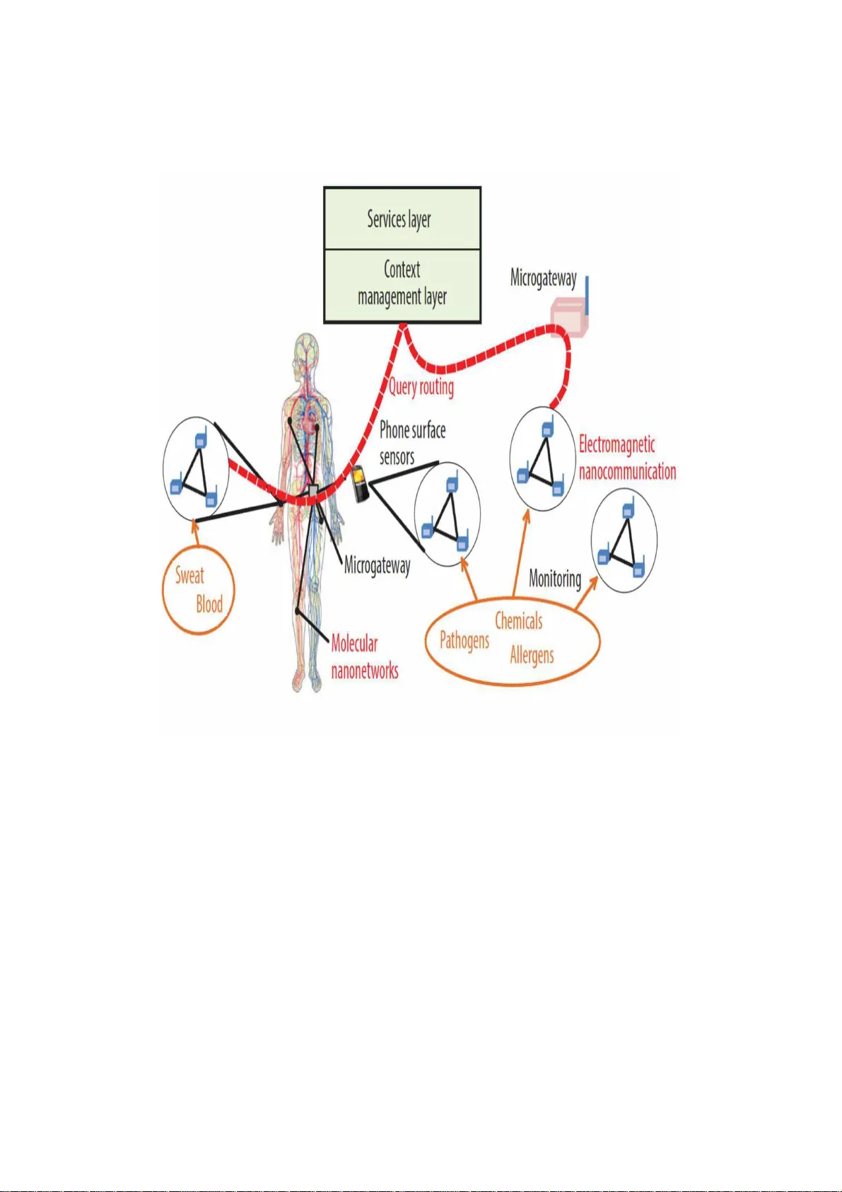
In ternet of NanoThings: Concepts and Applications Ebtesam Almazr ouei, Raed M. Sh ubair , and F abrice Saffre 2018 Con ten ts 1 In ternet of NanoThings 2 1.1 In tro duction to Nanonet w orks . . . . . . . . . . . . . . . . . . 3 1.1.1 Nanotec hnology . . . . . . . . . . . . . . . . . . . . . 3 1.1.2 Nanoscale Comm unication P aradigms . . . . . . . . . 4 1.1.3 Dev elopmen t of Nano devices . . . . . . . . . . . . . . . 6 1.1.4 Nano device Characteristic s . . . . . . . . . . . . . . . . 9 1.1.5 Wireless Nanodevice Arc hitectures . . . . . . . . . . . 10 1.2 The In ternet of NanoThings (IoNT) . . . . . . . . . . . . . . . 11 1.2.1 In ternet of Nano-Things . . . . . . . . . . . . . . . . . 11 1.2.2 Net w ork Arc hitecture . . . . . . . . . . . . . . . . . . . 14 1.2.3 Challenges of Nanoscale Comm unication . . . . . . . . 17 1.3 Applications of In ternet of NanoThings (IoNT) . . . . . . . . 22 1.3.1 The Inte rnet of Bio- NanoThings (IoBNT) . . . . . . . 22 1.3.2 Other Applications of IoNT . . . . . . . . . . . . . . . 24 References 28 1 Chapter 1 In ternet of NanoThings This c hapter focuses on In ternet of Things from the nanoscale p oint of v iew. The c hapter starts with section 1 whic h pro vides an introduction of nanoth- ings and nanotec hnologies. The nanoscale comm unication paradigms and the differen t a ppro ac hes are discuss ed for nano devices deve lo pmen t. Nano device c haracteristics are discussed and the arc hitecture of wireless nano devices are outlined. Section 2 describ es Internet of NanoThing(IoNT), its net w o rk ar - c hitecture, and the c hallenges of nanoscale comm unication whic h is essen tial for enabling IoNT. Section 3 gives some practical applications of IoNT. The in ternet of Bio-NanoThing (IoBNT) and relev an t biomedical applications are discusse d. Other Applications suc h as military , industrial, and en vironmen tal applications a re also outlined. 2 1.1 In tro ducti on to Nanonet works General Intro duction In 1959 , the Nob el phys icist Ric hard F e ynman stated the imp ortant ro le of tin y atoms and molecules size to dev elop fully functional an adv anced nano devices. The c hallenge of scaling the metria l in the ato ms nano scale w as highligh ted. Also, he entitled that the researc h in engineering will b e fo cused ho w to redesign or create nano comp onents in nanoscale devices. Now ada ys, curren t tec hnolog ies facing the c hallenge of how t o dev elop these nano com- p onen ts with taking in to consideration its nanoscale phenomena [1]. The term na no t ec hnology w as first in tro duced b y N. taniguc hi in 1974 as fo llows: “Nanotechnology mainly consists of the pro cessing of, separa- tion, consolidation, and deformation of materials b y one ato m or by one molecule.” [1, 2]. In 1986, K. Eric Drexler a ssociat ed the basic idea of F eyn- man’s vision ab out nano devices and added the concept of abilit y of creating these na no comp onen ts b y replicating themselv es using computer control in- stead of billion tiny facto r ies con trolled by h uman [1, 3]. Ho w ev er, the atten- tion from researc her to wards nanoscale comp onen ts has slo wly increase until the adv ancemen t starts to show o nly in the ear ly of 2000s. 1.1.1 Nanotec hnology Man y p eople could hav e confused b etw een the nanoscience and nanotec hnol- ogy . Nano technology is distinguished as applying the tech no logy to create no v el mat erials a t nano dimen tional scale based on the know ledge fro m the nanoscience. The nanoscience is defined as inv estigating the prop erties of the 3 material and it’s phenomena at the nano scale. The researc h intere st o f the kno wledge in nanoscienece and nano tec hnology is increased worldw ide. This enables exploiting new adv ance s materials, devices, and tec hnologies to w ork in few nano-meter length [4]. Nanotec hnology is a n emerging tec hnolog y pro viding a new sets to create and control the structure of the engineer- ing materials at nanoscale dimension for the aggrega tes of eac h individual molecules. Th is will enable the nano scale comp onen ts to p erform defined tasks suc h as data storing, sensing, computing, and actuation [5]. All the nano comp onents will b e in tegra ted in a single adv anced nano device. where this device will b e able to ac hiev e complex task in a distributed ma nner f o r health care, militar y , biological, a nd nanosensor netw ork [5 – 15]. 1.1.2 Nanoscale Comm un ication P aradigms The comm unication capabilities of nano devices plays vital role in the nan- otec hnology . It is imp o rtan t to enable accurate sync hronous b etw een nan- o devices that work in a co op erative and sup ervised en vironmen ts. The com- m unication in nano devices could b e divided t wo tw o categor ies as follows : • In ternal nano comm unication: Communic a tion b et we en t w o o r more of nano devices. • Ex ternal nano communication: Comm unication b et w een the nano de- vice and external system suc h as another electronic micro device. There are differen t comm unication tech no lo gies ha v e b een prop osed in the literature for nano devices suc h as electromagnetic comm unication, molecular comm unication, and acuastic comm unication [16, 17]. 4 Ele ctr omagnetic c ommunic ation uses electromagnetic w av es whic h propagates via air or wire with less losses. It is w ell used in micro electronics devices, but it has some limitations in implemen ting electromagnetic connec- tion through wires in nanoscale devices. Therefore, the electromagnetic com- m unication f or nano devices should b e implemen ted through wireless commu - nication. The wireless connection require nanoscale an tenna to b e dev elop ed for nano devices, also a radiof requency t ransceiv er should b e implemen ted in the nano device to establish bidirectional electromagnetic wireless comm uni- cation [16, 17]. Ho w ev er, the inte g ration of curren t ra dio t ransciv er is c hal- lenging due to the complexit y and the limitat ion of the size in nano devices. Also, the insufficien t output p o wer of nanotransive r a ffect the establishmen t of bidirectional connection b et we en nano devices. Hence, the electromagnetic w av es could b e used to send information from micro device to nanomec hine in one direction only . Therefore, another communication tec hnology should b e used to enable the internal communication among nano devices and the external commu nicatio n fr o m a nano device to a micro device [1 6 – 23 ]. A c oustic Communic ation is based on the transmission of ultrasonic w av es . The ultrasonic transducers are inte g r ated in the nano devices, there- fore there are able t o sense the ra pid v ariations of the pressure coming f r om ultrasonic wa v es; then acoustic signals are emitted [16 ]. Nanome chanic al c ommunic ati on pro vides the a bilit y to transmit the info r ma t ion thro ugh hard junctions b et w een link ed nano devices. This comm unication paradigm requires a phy sical link b et wee n transmitter and receiv er in the nano devices. In addition, the desired mec hanical transceiv ers should b e aligned precisely whic h is main drawbac k of this comm unication 5 paradigm as the nano devices will b e deplo y ed in nanonet work without an y direct or ph ysical con tact b et wee n them. Moreo v er, a precise navigation systems is needed to lo cate the nano devices in o rder to establish correct nanomec hanical comm unication [16]. Mole cular c ommunic ation is a new and promising tec hnolo g y that enables transmit and receiv e the data in molecules [16, 24 – 35]. The natural en vironmen t and the size of t he molecules make it is mor e feasible to inte- grate the molecular transceiv ers in nano devices. The nanotra nsciev ers are capable to release some molecules, react to ot hers , and resp onse to internak commands b etw een molecules in the nanonetw ork. 1.1.3 Dev elo p men t of Nano d evices A nanosensordevice is defined as a device designed f rom nano comp onen ts to p erform in nanoscale and able to establish a required task suc h as com- m unicate, sense, compute, store data, and actuate. These tasks p erformed b y nano comp onents and the complexit y of the dev elop ed-na no device relies on the lev el of t he requested task. Different approache s are used to dev elop the nano device: 1) the top down approac h, the b ottom-up a pproac h, and the bio-h ybrid approach as depicted in Figure 1.1 . T op-do wn approac h In the top down approac h, nano devices are dev elop ed b y downsc aling the cur- ren t micro electronic a nd micro-electro-mec hanical tec hnologies. Adv anced man ufacturing pro cesses are used to dev elop the nano device suc h as electron 6 Figure 1.1: Nano device approaches [1 6]. b eam lithogr a ph y [36 – 38] and micro-con tact prin ting [39]. The a rc hitec- ture of nano devices are kept same as the arc hitecture o f the micro electronic devices and micro-electro-mec hanical systems (MEMS). How ev er, the nano- electromec hanical systems approac h [4 0 – 42]. Simple mec hanical structures fabrication metho d such as nano - gears is prop osed for the fabrication and assem bly of these nano device follow ing this appro ac h but is still at an early stage [43, 44] Bottom-up approac h In the b otto m- up appro ac h, building blo ck s suc h a s individual molecules are used to dev elop nano devices. Nano devices has b een theoretically designed suc h as molecular differen tia l gears and pumps [51] based o n a discrete n um- b er of molecules [45]. This a ppro ac h is based on molecular man ufacturing tec hnologies where nano devices are assem bled molecule b y molecule. This 7 tec hnology is not av a ilable yet [16, 46, 47]. Currently there are differen t meth- o ds used to dev elop the nano devices follo wing b ottom- up appro a c h based o n self-assem bly molecular prop erties [48] suc h as molecular switc hes [49] and molecular shuttles [5 0 ]. Bio-h ybrid approac h Bio-h ybrid approa c h prop osed using the existing biological nano devices suc h as molecular motors, as building blo c ks or mo dels for the dev elopmen t of the new nano devices [51]. Most of the biological living organisms are exist in cells a s show n in Figure 1.1. The feat ur e of the biological structure of the living cell suc h as na no-biosensors, nanoactuators, bio lo gical data stor ing comp onen ts, to o ls and control units is expected to form new baseline of the manmade-nano device [16, 52]. Sev eral biological nano devices are in terconnected and form nanonet w or k. The inter-cell comm unication tec hnique allow s m ultiple cells to co op erate to p erform complex tasks suc h as cell division, the control of ho rmonal activities or imm une system resp onses in h umans. This o p eration of this biological nanonet w o r k is based on molecular signaling. The optimized arc hitecture, p ow er consumption, and comm unication paradigm of the existing biological na no devices motiv ates the dev elopmen t of the future nano devices using bio-h yprid approac h. 8 1.1.4 Nano device Characteristics The dev elopmen t of the future nano devices relies on the adv anced tec hnology that able to design the future nano devices whic h will b e a v ailable in the near future. The main characteris t ics of the future nano devices are detailed as follo ws [16]: • Self-con tained nano device: Each nano device has a co de o r set of in- structions to realize the in t ended ta sk. The co de or the instruction set can b e em b edded in the molecular structure of nano device or the nano device can read it from neigh b oured-molecular structure. • Self-asse mbly nano devices: Nano device can form an organized struc- ture from sev eral disordered elemen ts without external in terv ention, using the lo cal in teractions b et w een t hem. self-a ssem bly f eature is nat- urally found in molecular a ffinities b et w een tw o differen t elemen ts at nano lev el. This pro cess will enable the nano device t o in teract in an autonomous wa y with external molecules. • Self-replication: This c haracteristic should b e included in the nano de- vice to enable the nano device to cop y itself using external elemen ts. It implies that the nano device ha s set of instructions to create a copy of itself. This feature will facilitate the ability to realize macroscopic tasks b y creating large num b er of nano devices in an inexpensiv e w ay [53]. • Nanodevice-Comm unication: The comm unication b etw een nano devices is crucial to allo w nano devices to co op erate with eac h other in order to accomplish or realize more complex tasks. 9 • Locomotio n: Nano device mo ves fro m one place to another by spatial- temp oral actuation. Lo comotion will help the nano devices to p erfo rm sp ecific ta sks by iden tifying the nano device lo cation to b e at the rig h t place and the rig ht time to conduct the in tended task. Ho w ev er, the single nano device cannot mov e tow ards a previously iden tified target. Em b edded nanosensors and nanoprop ellers could b e used in a complex system to detect and trace the ta rget lo cation. This c haracteristics will optimize the use of nano r ob ots fo r disease treatmen ts in healthcare [54, 55]. F urther adv ances in nano -sensors and nano-actuators are exp ected to enable the in tegration of molecular transceiv ers in to nano-machine s. 1.1.5 Wirele ss Nano device A rc hitectures A wireless nano device could consists of one o r more comp onen ts based on the lev el of complexit y required to p erform in tended task. The architecture of nano device whether it is nanorob ot or simple molecular switc hes is as follo ws [16, 54]: 1. Con trol unit: Executes the instructions to p erform the requested tasks through con trolling all the other comp onen ts of the nano device. Also, the informat io n of the nano device could b e sa ved in a storage unit inside the control unit. 2. Comm unication unit: Enables the transmission a nd the reception of t he massages a t na no scale device e.g., molecules through nanotransceiv ers. 10 3. Repro duction unit: Utilizes external elemen ts to fabricate eac h nan- o device’s comp onen t and assem ble all the comp onen ts to replicate the nano device. All the instructions to conduct this ta sk are installed in the unit. 4. P ow er unit: Pro vides the p o wer to the en t ir e comp o nen ts in the nan- o device, harv ests energy from external sources,e .g ., temp erature, and ligh t. The energy is stored for a future needs of distribution and con- sumption. 5. Sensor and actuator s : Plays a role as in terface comp onen ts b et wee n the nano device and the en vironmen t and the nano-mac hine. There are v arious ty p es of sensors or actuators can b e enclosed in a nano device design suc h as c hemical sensors, temp erature sensors, pumps, clamps, motor or lo comotion mec hanisms. 1.2 The In te rnet of NanoThings (IoNT) 1.2.1 In ternet of Nano-Things The In ternet of Things (IoT) has ga ined a lot of inte r est from researc hers in the last decade. The ob j ectiv e is to extend the inte rnet to many device s and ob jects fr om differen t domains b y interconne cting those ob jects and devices with em b edded computing capabilities [56]. The w ord “things” includes a ll the physic al o b ject o n the planet not only comm unication devices to b e connected to the In ternet, and con trolled throug h wireless netw orks [57]. IOT devices will in terconnect through v arious ty p es of short-rang e wireless 11 tec hnologies suc h a s WiFi, radio f r equency identific a tion (R FID), Zig Bee, and sensor net w orks [58, 59]. The concept of IoT has attracted many researc hers w orldwide. It cov ers man y areas suc h as b o dy area net works, home area net w or ks, Unmanned Aerial V ehicle (UA V) net works, Device-to-Device (D2D) commun icat io ns, and satellite netw orks. Differen t net w or king pro t o cols, applications and net- w ork domains is expected to b e integrated to fit IoT tech no logies in the near future [5 7]. Securit y features and managemen t proto cols a re exp ected to b e added to IOT link ed net w orks and devices [59]. In IoT,all t yp es of real phys ical elemen ts suc h as a ctuators and sensors, p ersonal or home electronic devices are connected amo ng others whic h en- able new era of seamless connectivit y for v arious applications suc h as ma- c hine to mac hine ( device t o device) comm unicatio n, real time monitoring for health care and industrial en vironment, v ehicle to v ehicle communica- tion and transp ortation, smart grids and infrastructures to establish smart energy managemen t, infra structure management, en vironmen tal monitoring, in telligen t health monitoring, in telligent transp ort a tion o n larg e grid [56]. This is ac hieve d by incorp orating nano devices to b e in terconnected using nanonet w o r ks. Figure 1 .2 illustrates the concept of nanonet works in health- care application. Implemen ting nano devices facilitates the abilit y to sense and collect data data fr om pla ces in the b o dy that previously imp ossible to sense due to sensor size. Th us, new medical diagno stics and disco ve r ies will adv ance the curren t medical tec hnology [60]. Akyildiz et al. define this tech no lo gy as In ternet of Nano Thing (IoNT) [61]. 12 Figure 1.2: The Internet of Nano Things [60]. The concept of the IoNT is in tro duced as a ty p e o f IoT where nano de- vices whose dimensions may range from 1 to 100 nm are in terconnected with classical netw orks leading to new net w o r king para dig ms. Graphene-based nanoan tennae is prop osed to b e utilized in IoNT tec hnolog y and o p erating at T erahertz frequency band [61]. The problem of extreme atten uation of tetrahertz frequencies in na noscale device is outlined by [61]. IoNT faces c hallenges to interface the curren t micro devices netw orking with the new 13 nano devices sc heme. Therefore, ma j o r researc h should b e conducted to ad- dress the communic a tion and net workin g c hallanges in electromagnetic field, the c hannel mo delling, and the required net workin g proto cols to op erate in IoNT for v arious industrial, biomedical a nd industrial applications. 1.2.2 Net w ork Arc hitecture The w ork conducted by Akyildiz et al. fo cuses on electromagnetic commu- nication for the IoNT net w orks [61] in in tra b o dy nanonet works f or remote healthcare, and the interconnec t ed office. The net w ork archite cture sho ws in Figure 1.3 is comp osed of nano-no des, nano-routers, nano mac hines suc h a s nanosensors and nanoactuators whic h deplo y ed in the h uman b o dy to pro - vide the examiner or the healthcare pro vider t he ability to access and con trol the nano devices remotely through nano micro in terface devices [6]. Addition- ally , Akyildiz et al. show s the in terconnected office architec t ure where eac h single elemen t fo und in the office is pro vided with nanotransciev er to allow them to sta y p ermanen tly connected to the interne t . Therefore, the lo cation and the status of the all elemen ts in the office ar e trac k ed in a n effortless manner. How ev er, an ultra-low p o wer consumption and reasonable comput- ing capabilities are required for the nano devices to harv est the mec hanical and electromagnetic energy from the environme nt and k eep the function with high p erformance [6, 62]. Ho w eve r , eac h nanonetw ork has fundamen ta ls comp onen ts in the net w o r k arc hitecture of the Internet of Nano-Things as follow ing [6 1]: 14 Figure 1.3: Netw ork architec ture for the In ternet of Nano-Things [61]. Nano No des Nanono des are the smallest and simplest na no ma chines in the nanonet w o rk arc hitecture. Simple computation tasks a re assigned to them b ecause of their limited memory . There is limitation in their comm unication capabilities and consumption energy , therefore they are able to transmit for short range distances. Nanono des could b e implemen ted in a ll t yp es of things suc h as b o oks, k eys, pap er folders, or inside the human b o dy as biolo gical nanosensor no des. Nano Routers Nanorouters are capable for aggregating the information coming f rom lim- ited nano mac hines. It is used to con trol the b eha vior of nano no des by ex- c hanging simple con tro lling commands suc h as: on/off switc hing, read v alue, sleep, etc.). Nanorouters ha ve larger computatio na l resource s than nanon- 15 o des, how ev er, the increase in capa bilities leads to increase in their size whic h affect the their deplo ymen t in the nanon tw ork. Nano-micro Interface Devices Nano-micro inte rf ace devices are implemen ted to enable the receiv e/send information coming from nanor outers to the microscale device or system and vice ve r sa. Nano- micro interface devices could b e hyb r id devices able to comm unicate in the nanoscale using t he classical communication para digms in con ven tional comm unication net w or ks and new communic a tion paradigm for nano devices net w ork. Gatew a y Gatew ay facilitates the remote connection of the en tire system o ve r t he In- ternet. F or example, in an in trab o dy net work scenario in healthcare era, an adv anced cellphone can forward the receiv ed informa t io n from nano-micro in terface device to the end user ( healthcare provider in this example). A mo dem-router is utilized in interconnecte d office to establish this function- alit y . it receiv es fr o m a nano-micro in terface in our wrist to our healthcare pro vider. In the interconne cted office, a mo dem-router can provided t his functionalit y . Despite the in terconnection of microscale devices, the deve l- opmen t o f gatewa ys and the net work management ov er the In ternet are still op en researc h a reas, in the remaining of this article w e mainly fo cus on the comm unication c hallenges among nanomachine s. Moreo v er, the w ork by Balasubramaniam et al. fo cuses o n wireless b o dy area net w o rks constructed by nano devices [2]. The b o dy area netw orks col- 16 lect vital pat ient information and feed tho se information to service provide rs’ computing systems . As a consequence , it a c hiev es higher accuracy and ef- ficiency in monitoring the health conditions of a large num b er of patien ts. Moreo v er, sensors em b edded in t he en vironmen t can passiv ely assist daily life of the elderly and disabled p eople. With the dev elopmen t of small device s and their comm unications p erformance, suc h netw orks in tiny area are also exp ected to b e required in the future. 1.2.3 Challenges of Nanoscale Comm un ication The Interne t of Nano- Things requires redesign and dev elop new comm u- nication paradigms, and net working concepts that will b e compatible for nanoscale mac hines. Many comm unication c hallenges app ear in the phys - ical lay er of nanomac hines to t he nanonetw orking proto cols. This section highligh ts the main c hallenges from comm unication respectiv e as discussed in [61]. F requency Band of Op eration of Electromagnatic Nano-transceiv ers The comm unication opp ortunities and c hallenges at the nanoscale devices are strongly asso ciated with the op erat ing frequency ba nd of the nano- transciv er esp ecially nano-an tennas. Theses future an t ennas are predicted t o b e man- ufactured using nov al material as graphene for nano comm unication net- w ork [6 1, 63, 64]. The ve lo cit y of wa v e propagation in grahene-nano a n tenna is scaled to b e one hundred times b elo w the sp eed of light in v acuum. Addi- tionally , the resonan t frequency na noan tenna built with gr aphene can b e up 17 to tw o o r ders of magnitude b elo w that nanoan tennas based ob non-carb on materials. In particular, Lin et al. found that a 1 µ m long graphene-based nano- an tenna built either by gra phene nanor ibb on (GNR) or carb on nanotub e (CNT) radiat es efficien tly in T erahertz range whic h satisfies the predication of frequency band f or graphene-based RF transistors [65]. In [66], it has b een sho wn that a single carb on na notub e t ha t mec hanically resonates at the w av e frequency is able to receiv e and demo dulate an electromagnetic w av e. This single CNT ante nna has designed with one end connected to v ery high v olta ge source and the other end is left floa ting. The electrons at the free tip end vibrate when the nanot ub e is irradiated b y an EM w av e. Th us, there will b e frequency initiated by EM w av e and if it matc hes the natural resonan t frequency of the CNT antenna, these vibrations b ecome significan t and enable the single CNT an tenna to receiv e and demo dulate the signal. The EM w av es generated b y CNT-based nano- mec hanical receiv er can op erated ab ov e few micrometers. Ho w ev er, the energy efficiency is predicted to b e very low to generate EM w av es in nano antennas radiated in T erahertz band [6 7]. Also, a high p o w er source is required to excite the CNT an tenna mec hanically whic h is inefficien t for g enerating the f utur e EM nanonet w o rks op erating in the T erahertz band. Nev ertheless, CNT-based nano- mec hanical receiv er can b e used in the nanonet w ork to con trol the nano devices from the macro and microscale in nano- micro interface devices. As an example, a con- v en tional AM/F M transmitter can b e used to activ ate/deactiv ate thousands of nano devices sim ultaneously . 18 The far infrared band and the microw a v es frequency ba nd whic h is ab ov e and b elo w, respectiv ely the T etrahertz band hav e been extensiv ely inv esti- gated. The T erahertz ba nd is one he least-explored frequency zones in the EM sp ectrum. Therefore, the new c hannel mo dels for the T era hertz band should b e dev elop ed for electromagnetic nanonetw orks. Channel Mo deling The T erahertz ba nd spans the frequencies b et wee n 100 GHz and 10 THz is still unlicensed band. It ha s ma jor limitatio ns for short and medium range comm unications [68, 69] but but it is applicable for nanonetw ork applications as discussed aforemen tio ned, therefore the c hannel mo delling for this band in the v ery short range should b e in ve stigat ed. Jornet et al. in v estigates the prop erties of the T erahertz band in terms of path- loss, noise, bandwidth and c hannel capacit y as describ ed b elow [69]. • P ath-loss The total path-lo ss L ( f w , l path ) for a tra v elling wa v e in the T erahertz band is defined as the addition of the spreading loss L spr ead and the molecular a bsorptio n loss L absorbtion . L ( f w , l path ) = L spr ead ( f w , l path ) + L absorbtion ( f w , l path ) (1.1) where f w is the frequency w av e in T etrahertz ba nd and l path is the tota l path length of the w av e. The spreading loss is a result of t he atten uatio n coming from the ex- pansion o f the frequency w a ve f w as it pr o pagates through the medium 19 l path . L spr ead ( f w , l path ) = ( 4 π f w l path c ) 2 (1.2) where c is the sp eed of ligh t in a v acuum. The absorption lo ss L absorbtion is a result of the atten uation o ccurs b e- cause of the molecular absorption that aff ects t he propagation wa v e. The w a ve energy con v erts to kinetic energy of the excited mo lecules b y electromagnetic radiatio n at certain frequencies within the t era hertz band where pa rt of the radiat io n conv erts to internal vibration. Thus , the wa v e energy reduced leading to the absorptio n lo ss L absorbtion and it defined as follow s: L absorbtion ( f w , l path ) = 1 e − k ( f w ) l path (1.3) where k is the medium absorption co efficien t. The absorption loss dep ends on t he ty p e of the molecules and it s con- cen tration a long t he path. Differen t resonance frequency asso ciated to differen t t yp es o f molecules where the absorption at each resonance spreads ov er a rang e of frequencies. As a consequence, the T erahertz c hannel will suffer from high fr equency selectivit y , m ulti- path propa- gation, and scattering from the nano particles in the field whic h affect the signal strength at the receiv er. • Noise The main source of the am bient noise in t he T erahertz ba nd is the 20 molecular noise. The molecular absorption in t r o duces noise alo ng with the atten uation. This t yp e o f noise o ccurs only when transmitting signal t hrough the c hannel. Additionally , equiv alen t noise temperat ure is in tro duced around the frequencies where the molecular absorption is considered high. The total noise p o we r at the receiv er is computed as follo ws: P noise ( f w , l path ) = k B B ( T molecul ar ( f w , l path ) + T else ( f w )) (1.4) where k B refers to the Boltzmann constan t, B is the system tra ns- mission bandwidth, T molecul ar is the the molecular noise tempera t ur e, and T else stands for other noise source presen t in the medium, e.g., electronic noise of the receiv er. The total noise p ow er P noise has sev eral p eaks of noise in the sp ectrum due to the differen t r esonant frequencies associated with eac h t yp e o f molecules [69]. • Band widt h and chann el capacit y The molecular absorption determines the transmission bandwidth in T erahertz c hannel. Therefore, the molecular comp o sition of the medium and the tota l transmission path constrain the a v ailable bandwidth. The a v ailable bandwidth for a v ery short range is ranging fro m a few h un- dreds of gig ahertz to almost ten T erahertz (almo st the en tire band). Therefore, the c hannel capacity of electromagnetic nanonet works in the T erahertz band is predicted to b e in the order of a few terabits 21 p er second. Ho w ev er, t here is limitation in the transmitted info rma- tion capacit y due t o limitatio n in the capabilities of nanomachines or nano devices whic h do es not mak e use of this large bandwidth. Despite of this limitation, the a v ailable bandwidth could op en new r esearc h for new information mo dulation tec hniques and channe l sharing sc hemes, sp ecially designed for nano device in the nanonetw orks op erating in the T erahertz band. 1.3 Applicatio ns of In terne t o f NanoThing s (IoNT) 1.3.1 The In ternet of Bio-NanoThings (IoBNT) A nov a l researc h directed to wards implemen ting nano devices and nanotec h- nology in the biological field. There is increased in terest to merge the to ols from syn thetic biology within the nanotec hnolog y to con trol, mo dify , reengi- neer, and reuse the biological cells [56, 70]. The biological cell whic h is utilized in IoT embedded computing device is called Bio-NanoThing (BNT) where it can effectiv ely control, reuse, a nd reengineer the functionalities of biological cells suc h as sensing, actuation, pro cessing, and comm unication. This con- cept introduced t he In ternet of Bio-NanoThing (IoBNT) where the cells a r e based on biolog ical molecules instead of electronics. 22 Biomedical Applications IoBNT enables compatibilit y and stabilit y at the bio -molecular lev el. This pro vides the abilit y to use IoNBT to inte r a ct with organs and tissues. In this section, IoBNT a pplicatio ns are men tio ned [16]. • Imm une system supp ort IoBNT can b e utilized to supp ort the imm une sys tem to iden tify and con trol foreign a nd pathogen elemen ts in the h uman b o dy . Sev eral nano devices suc h as sensors and actuators collab orate with eac h other in macro, micro, and na no systems to protect organism ag a inst diseases. Implemen ting nano devices can adv anced the medical field by utilizing theses nano devices to predict, detect, and eliminate certain pro cedures based on lo calization of malicious agents and cells, such as cancer cells [71, 72]. This will minimize the risk of deve lo ping suc h disease and pro vide treatmen ts less aggressiv e a nd in v asiv e compar ed to the existing ones. • Bio-h ybrid implan ts Nanonetow rks in IOBNT will support the re- placemen t of organs, nerv ous trac ks, or lo st tissues in the hum a n b o dy [46, 73 ]. F riendly in terfa ces can b e pro vided b etw een the bio- h ybrid implan ts a nd the environmen t whic h enable the restoration of cen t r al nerv ous system track s. • Drug deliv ery systems Nanp devices in IoBNT can b e used as regu- later implan ts that could comp ensate metab olism diseases such a s dia- b etes.Smart glucose reserv oirs and nanosensors collab ora t e to supp ort 23 the glucose lev el mec hanisms [74, 75]. The effects of neuro degenera- tiv e diseases can b e eleminated using drug delive ry system to deliv er neurotransmitters or sp ecific drugs to neurosystem [76]. • Health monitoring Implemeting nanosensor netw orks in human b o dy can b enefit the medical field b y prov ide health monito r ing to monitor and con trol Oxygen, choleste r o l leve l, and hormonal disorders, and pro vide early diagnoses of the health status [73, 77]. A go o d lev el of connectivit y should b e main tained b et we en the nanonet work and t he actors who can access the transferred health informatio n. • Genetic engineering The use of nanonet w o r ks in IoNBT will allo w the p oten tial increase o f genetic engineering applicatio ns. Nano devices will enables t he mo dification, re-engineering, and manipulation of nano- structures inside g enes and molecular sequenc es [16]. 1.3.2 Other Applications of IoNT Industrial A pplications Nanonet w o r k will b e used in the industrial and consumer go o ds applications. It will adv ance the manufacturing pro cesses, the dev elopmen t of new materi- als, and the quality control pro cedures. More sp ecifically , these applications ha v e already b een prop osed b y [56]: • F o o d and wa t er qualit y control Nanonetw orks could b e used t o monitor and control the fo o d and fluids qualit y . Nanosensor will b e able to detect the t o xic comp onen ts and small bacteria found in the fo o d and 24 w ater that can not b e detected using traditional sensing tec hnologies [78]. This adv anced self-p o were d nanosensor net works will b e able ev en to sense the tiny amount of defects suc h a s c hemical or biolog ical a gen ts installed in w ater supplies [56]. • F unctionalized materials and fabrics New adv anced materials and fabrics can b e manufactured by using nanonetw orks in order t o im- pro ve certain f unctionalities. There are dev elop ed pro ducts suc h a s an timicrobial and stain- rep eller textiles using nanofunctionalized ma - terials [79, 80 ]. Nano actuators comm unicate with nanosensors in or der to con trol the reaction which will impro v e the airflow in adv ance d smart fabric. Military Applications Nanothec hnology can emphasize and adv ance sev eral applications for mili- tary field. Nanonet work rang e is short; therefore the range of nanonet w o r ks is sp ecified based on the required application. The range of nanonet works for monito ring soldier p erformance applications is small within hum a n b o dy range while for a dense lar g e net work is required for ba t t lefield monitoring and actuation. Belo w a re some of the military applications: • Nuclear, biological, and c hemical (N BC) defenses F or la rge area o v er the battlefield o r targeted areas, a dense net w o r k consists of nanosensors and nanoactuators is deploy ed to detect a g - gressiv e c hemical a nd biological agen t s. Additionally , it co ordinates the defensiv e resp onse battlefield areas [16, 81]. Nanosensor netw orks 25 can b e used b e to detect the unautho rized en t r a nce biological, c hemical, and radiolog ical mat erials installed in the cargo containers. • Nano- functionalized equipmen ts Nano netw orks can adv anced the camouflage and army uniforms using new adv anced military equip- men ts than can manufacture adv anced materials equipeed with nanonet- w orks. This tec hnolo gy will enable the self-regulation o f soldiers’s b o dy temprature underneath his clothes and will b e able to detect and inform if the t he soldier has b een injured [82]. En vironmen tal Applications Nanonew orks ha ve v arious application in en vironmen tal fields that will ad- v ance the curren t technologies. Some en vironmen tal applications are men- tioned as fo llo ws [16]: • Biodegradation The rising problem of g arbage handling around the w orld, bio degradation pro cess in the garbag e dumps using nanonet- w orks could manage the problem. Nano net works can b e used to sense and tag differen t materials, then smart nanoactuators are utilized to lo cate and pro cess the bio degradation for theses materials. • Anima ls and bio diversit y con t rol Sev eral animal sp ecies can b e con trolled by nanonet w o rks in natural environme nts. Nanonet w o rks could dev elop pheromones or messages to trigger certain animals b e- ha viors. Therefore, controlling the lo cation of certain animal sp ecies in particular env iro nmen t w ould b e p ossible. 26 • Air p ollution control The quality of air can b e managed and con- trolled b y nanonetw orks. Adv anced nano filters will b e dev elop ed to remo v e harmful substances or c himicals in the air whic h will impro ve the air qualit y [83]. Also, the nanofilters can be used for water qual- it y [84]. 27 References [1] I. F . Akyildiz, J. M. Jornet, and M. Pierob on, “Nanonetw orks: A new frontier in comm unications,” Communic ations of the ACM , v ol. 54, no. 11, pp. 84–89, 2011. [2] N. T aniguc hi, “On the basic concept of nano-tec hnology pro ceedings of the international conference o n pro duction engineering tokyo part ii japan so ciet y of precision engineering,” 1974 . [3] K. DREXLER, “Molecular engineering- a ssem blers and future space hardw are,” A er osp ac e c entury XXI: Sp ac e scienc es, applic ations, and c ommer cial develop m ents , pp. 1 327–1332, 1987 . [4] B. Ro szek, W. De Jong, and R. Geertsma, “Nanot echnology in medical applications: state-of-t he- a rt in materials a nd devices,” 2005. [5] I. F. Akyildiz and J. M. Jornet, “Opto electronics & comm unications nanoscale broadband terahertz comm unication.” [6] —— , “Electromagnetic wireless nanosensor net w o r ks,” Nano Com mu- nic ation Networks , v ol. 1, no. 1, pp. 3–19, 2010. 28 [7] R. M. Sh ubair , “Ro bust adaptiv e b eamforming using LMS algor it hm with SMI initializatio n,” in 2005 IEEE Antennas and Pr op agation So- ciety International Symp osium , v ol. 4A, Jul. 2005 , pp. 2–5 v o l. 4A. [8] R. M. Shubair and W. Jessmi, “P erformance analysis of SMI adaptive b eamforming a r r a ys for smart an tenna systems,” in 2005 IEEE A n ten- nas and Pr op agation So ciety International S ymp osium , v ol. 1B, 2005, pp. 311–3 14 vol. 1B. [9] F. A. Belhoul, R. M. Sh ubair, and M. E. Ai-Mualla, “Mo delling and p erformance analysis of DO A estimation in adaptiv e signal pro cessing arra ys,” in 10th IEEE I nternational Confer enc e on Ele ctr onics, Cir cuits and Systems, 2003. ICECS 2003. Pr o c e e ding s of the 2003 , vol. 1, Dec. 2003, pp. 3 40–343 V ol.1. [10] R . M. Sh ubair and A. Al- Merri, “Robust algo rithms for direction find- ing and adaptiv e b eamforming: p erformance and o pt imizatio n,” in The 2004 47th Midwest Symp osium on Cir cuits and Systems, 20 0 4. MWS- CAS ’04 , v ol. 2, Jul. 2004, pp. I I–589– I I–592 v ol.2. [11] E. Al-Ardi, R. Sh ubair, and M. Al-Mualla, “Direction of a r riv al estima- tion in a multipath en vironment: An ov erview and a new con tributio n,” in ACES , v o l. 21, 200 6. [12] G . Nw alozie, V. Ok or o gu, S. Maduadic hie, and A. Adenola, “A simple comparativ e ev aluation of a daptiv e b eam forming algorithms,” I nterna- tional Journal of Engin e ering and I nnovative T e chnolo gy (IJEI T ) , v ol. 2, no. 7, 20 1 3. 29 [13] M. A. Al-Nuaimi, R. M. Sh ubair, and K. O. Al-Midfa, “Direction of arriv al estimation in wireless mobile comm unications using minim um v ariance distortionless resp onse,” in Se c ond Internation al Confer enc e on Innovations in Information T e c h nolo gy (IIT’0 5) , 2005, pp. 1–5. [14] M. Bakhar and D. P . Hunagund, “Eigen structure based direction o f arriv al estimation a lg orithms fo r smart antenna systems,” I JCSNS In - ternational Journal of Com puter Scienc e and Network S e curity , v ol. 9 , no. 11, pp. 96–100, 2009. [15] L. Mohjazi, M. Al-Qutay r i, H. Barada, K. P o on, a nd R. Sh ubair, “ De- plo ymen t c hallenges of fem to cells in future indo or wireless net w orks,” in GCC Confer enc e and Exhibition (GCC), 2011 IEEE . IEEE, 2 011, pp. 405–408. [16] I. F. Akyildiz, F. Brunetti, and C. Bl´ azquez, “Nanonetw orks: A new comm unication para digm,” Computer Networks , v ol. 52 , no. 12 , pp. 2260–227 9, 2008. [17] R . A. F reitas, Nanome dicine, volume I: b asic c ap abilities . Landes Bio- science Georgetown, TX, 1999. [18] M. S. Khan, A. D. Cap obianco, S. M. Asif, D. E. Anagnostou, R. M. Sh ubair, and B. D. Bra aten, “A Compact CSRR-Enabled UWB Di- v ersit y An tenna,” IEEE A ntenna s and Wir eless Pr op agation L etters , v ol. 1 6, pp. 808– 8 12, 20 17. 30 [19] R . M. Sh ubair and Y. L. Chow , “A closed-form solution of vertical dip ole an tennas ab ov e a dielectric half-space,” I EEE T r ansactions on Antennas and Pr op agation , v o l. 41, no. 12, pp. 173 7–1741, Dec. 199 3. [20] A. Omar and R . Sh ubair , “UWB coplanar w av eguide-fed-coplanar strips spiral an t enna,” in 2016 10th Eur op e an Confer enc e on Antennas and Pr op agation (EuCAP) , Apr. 2016, pp. 1–2. [21] M. AlHa jri, A. Goian, M. Darw eesh, R. AlMemari, R. Sh ubair, L. W eru- aga, and A. AlT unaiji, “Accurate and robust lo calization tec hniques for wireless sensor netw orks,” June 2 018, arXiv:1806.05 765 [eess.SP]. [22] J. Samhan, R. Shubair, and M. Al-Qutayri, “Design and implemen tation of an adaptiv e smart an tenna system,” in Innovations in I n formation T e chnolo gy, 20 06 , 2006, pp. 1–4. [23] M. AlHa jri, A. Goian, M. Darw eesh, R. AlMemari, R. Sh ubair, L. W eru- aga, a nd A. Kulaib, “ Hybrid rss-doa tec hnique for enhanced wsn lo cal- ization in a corr elated env iro nmen t,” in Information and Communic a- tion T e chnolo gy R ese ar ch (ICTRC), 201 5 In terna tion a l Confer enc e on , 2015, pp. 2 38–241. [24] R . M. Sh ubair and H. Elay an, “In viv o wireless b o dy commun icatio ns: State-of-the-a r t and future directions,” in Ant e n nas & Pr op agation Con- fer enc e (LAPC), 20 1 5 L oughb or ough . IEEE, 2015, pp. 1–5 . [25] H. Elay an, R. M. Sh ubair, J. M. Jor net, and P . Johari, “T erahertz chan- nel mo del and link budget analysis f or intrabo dy nano scale commu nica- 31 tion,” IEEE tr ansactions on nanobioscien c e , vol. 16 , no. 6, pp. 49 1 –503, 2017. [26] H. Ela y an, R. M. Shubair, a nd A. Kio urt i, “Wireless sensors for medical applications: Curren t status and future c hallenges,” in A ntenn a s and Pr op agation (EUCAP), 2017 11 th Eur op e an Conf e r enc e on . IEEE , 2017, pp. 2 478–2482 . [27] H. Ela y a n and R. M. Shubair, “On channel ch a racterization in hu- man b o dy comm unication for medical monitoring systems,” in Antenna T e chnolo gy and Applie d Ele ctr omagnetics (ANTEM), 2016 17th Inter- national Symp osium on . IEEE, 2 0 16, pp. 1–2 . [28] H. Elay an, R . M. Sh ubair , A. Alomain y , and K. Y ang, “In-viv o terahertz em c hannel c ha racterization for nano-comm unications in wbans,” in An- tennas an d Pr op agation (APSURSI) , 2016 IEEE International Symp o- sium on . IE EE, 2016, pp. 97 9–980. [29] H. Elay an, R . M. Shubair, and J. M. Jornet, “Bio- electromagnetic thz propagation mo deling for in-viv o wireless nanosensor netw orks,” in A n- tennas and Pr op a g ation (EUCAP), 2 017 11th Eur op e an Confer enc e on . IEEE, 2017, pp. 426–430 . [30] M. J. Mo ore, A. Enomoto, T. Na k ano, R. Egashira, T. Suda, A. Kay a- suga, H. Ko jima, H. Sak akibara, and K. Oiw a, “A design of a molecular comm unication system for nanomachine s using molecular motors.” in PerCom Workshops , 2006 , pp. 554–559. 32 [31] H. Elay an, C. Stefanini, R. M. Shubair, and J. M. Jornet, “End-to-end noise mo del for intra-b o dy terahertz nanoscale communic at ion,” IEEE T r ansactions on NanoBioscienc e , 2018. [32] H. Elay an, P . Johari, R. M. Shubair, and J. M. Jornet, “Photother- mal mo deling a nd analysis of intrab o dy terahertz nanoscale comm unica- tion,” IEEE tr ansactions on nanobioscien c e , vol. 16 , no. 8, pp. 75 5 –763, 2017. [33] H. Ela yan, R. M. Sh ubair, J. M. Jo r net, and R. Mittra, “Multi- lay er in trab o dy terahertz w a v e propagation model for nanobio sensing appli- cations,” Nano Co m munic ation Networks , vol. 14, pp. 9–1 5, 2017. [34] H. Elay an, R. M. Shubair, a nd N. Almo osa, “In viv o communication in wireless b o dy a rea net works ,” in Information Inn ovation T e chnolo gy in Smart Cities . Springer, 20 1 8, pp. 273– 2 87. [35] M. O. AlNab o o da, R. M. Sh ubair, N. R. Rishani, and G . Aldabbagh, “T erahertz sp ectroscop y and imaging for the detection and iden tification of illicit drugs,” in Sensors Networks Smart and Emer ging T e chnolo gies (SENSET), 2017 , 2017, pp. 1–4. [36] A. A. Tseng, K. Chen, C. D. Chen, and K. J. Ma, “Electron b eam lithograph y in nanoscale fabrication: recen t dev elopmen t,” I EEE T r ans- actions on ele ctr onics p ackaging manufacturing , vol. 26, no. 2, pp. 1 4 1– 149, 2003. 33 [37] M. J. Burek and J. R. Greer, “F abrication and microstructure con trol of nanoscale mec ha nical testing specimens via electron b eam lithograph y and electroplating,” Nano letters , v ol. 10, no. 1, pp. 69–76 , 2009. [38] P . Emami, “Electron b eam lithograph y for nano-antenna f a brication,” Ph.D. dissertation, Univ ersit y of Missouri–Colum bia, 2015. [39] H. H. Lee, E. Menard, N. G. T assi, J. A. Rogers, and G . B. Blanch et, “Large area micro contact printing presses fo r plastic electronics,” in MRS Pr o c e e dings , v ol. 846. Cam bridge Univ Press, 2004, pp. D D7–3. [40] C.-Y. Chang, “The highligh ts in the na no w orld,” Pr o c e e din gs of the IEEE , v ol. 91, no. 11 , pp. 175 6 –1764, 200 3. [41] H. Goldstein, “ The race to the b o ttom [consumer nano device],” I EEE Sp e ctrum , v ol. 42, no. 3 , pp. 32 –39, 20 05. [42] M. Meyy appan, J. Li, J. Li, and A. Cassell, “Nanotec hnology: An o ve rview and in tegration with mems,” in Pr o c e e dings of the 19 th IEEE International Confer enc e on Micr o Ele ctr o Me chanic al Systems (MEMS’06) , 2006, pp. 1–3. [43] Y. J. Y un, C. S. Ah, S. Kim, W. S. Y un, B. C. Park, and D. H. Ha, “Manipulation of freestanding au nanogear s using an atomic force mi- croscop e,” Nanote chnolo gy , v ol. 18, no. 50, p. 505304, 2007. [44] W.- H. So e, C. T roadec, C. Manzano, J. Deng, F. Ample, Y. Jia nsh u, and C. Joac him, “Nanogears mec hanics: F rom a single molecule to solid- 34 state na nogears o n a surface,” in Single Mole cular Machines and Motors . Springer, 2015 , pp. 187–196 . [45] C. Pe terson, “T aking tec hnology to the molecular lev el,” Computer , v ol. 3 3, no. 1, pp. 46–53, 200 0. [46] K. E. D rexler, Nanosystems: mole cular machine ry, manufacturing, an d c omputation . John Wiley & Sons, Inc., 1992. [47] E. L. W olf, Nanop hysics and nanote chnolo gy: An intr o duction to m o dern c onc epts in nanoscie n c e . John Wiley & Sons, 2015. [48] V. Ba lzani, A. Credi, S. Silvi, and M. V en turi, “Artificial nanomac hines based on in terlo c k ed molecular sp ecies: recen t adv ances,” Chemic al So- ciety R eviews , v ol. 35, no. 11, pp. 1135–11 4 9, 2006. [49] R . Ballardini, V. Ba lzani, A. Credi, M. T. Gandolfi, and M. V en turi, “Artificial molecular-lev el mac hines: which energy to mak e them w ork?” A c c ounts of Chemic al R ese ar ch , v ol. 34, no. 6, pp. 445–455, 2001. [50] V. Ba lzani, M. G´ omez-L´ op ez, and J. F . Sto ddart, “Molecular machine s,” A c c ounts of Chemic al R ese ar ch , v ol. 31, no. 7, pp. 405–414, 1998. [51] G . M. Whitesides, “The once and future na nomac hine,” Sc ientific Amer- ic an , vol. 285, no. 3, pp. 70–5, 2001 . [52] D . K. Eric, P . Chris, and P . Gayle, “ Unbounding the f ut ure: the nan- otec hnology rev olution,” Pr o duc e d for the Web by E-SP ACES. New Y ork , 1991 . 35 [53] R . MERKLE, “Self replicating systems and molecular man ufacturing,” British Interpla netary So ciety, Journal , v ol. 45, no. 10, pp. 407– 413, 1992. [54] A. Cav alcanti, B. Shirinzadeh, R. A. F reitas Jr, and T. Hogg, “Nanorob ot ar chitecture fo r medical ta rget identification,” Nanote ch- nolo gy , vol. 1 9, no. 1, p. 015103, 2007. [55] G . Muth ukumaran, U. Ramac handraiah, and D . Sam uel, “Role o f nanorob ots and their medical applications,” in A dvanc e d Materials R e- se ar ch , v o l. 1086. T r a ns T ec h Publ, 2015 , pp. 6 1–67. [56] I. Akyildiz, M. Pierob on, S. Ba lasubramaniam, and Y. K ouc hery avy , “The inte rnet of bio-na no things,” I EEE Com m unic ations Magazine , v ol. 5 3, no. 3, pp. 32–40, 201 5. [57] Y. Kaw amoto, H. Nishiy ama , N. YOSHIMURA, and S. Y AMAMOTO, “In ternet of things (io t ): Presen t state and future pro sp ects,” IEIC E TRANSA CT I ONS on Information and Systems , vol. 97, no. 1 0 , pp. 2568–257 5, 2014. [58] M. A. F e ki, F. Kaws ar , M. Bo ussard, and L. T rapp eniers, “Guest edi- tors7 in tro duction,” 20 1 3. [59] M. H. Miraz, M. Ali, P . S. Excell, a nd R. Pic king, “A review on in ternet of things (io t), in ternet of every thing (io e) and interne t of nano things (ion t),” in Internet T e chnolo gies a nd Applic ations (IT A), 201 5 . IEEE, 2015, pp. 2 19–224. 36 [60] S. Balasubramaniam and J. Kangasharju, “Realizing the interne t of nano things: challen g es, solutions, and a pplications,” C omputer , vol. 46, no. 2, pp. 62–68, 2013. [61] I. F. Akyildiz and J. M. Jornet, “The in ternet of nano-things,” IEEE Wir eless Co mmunic ations , v o l. 1 7 , no . 6, pp. 58 – 63, 20 10. [62] Z . L. W ang, “T o wards self-p o we red nano systems: fr om nanogenerators to nanopiezotronics,” A dvanc e d F unctional Materials , v o l. 18 , no. 22, pp. 3553– 3567, 2008 . [63] J. M. Jornet and I. F. Akyildiz, “ G raphene-based nano-ante nnas for electromagnetic nano communic a tions in the terahertz band,” in Pr o- c e e di n gs of the F ourth Eur op e an Con f e r enc e on Antennas a nd Pr op ag a- tion . IEEE, 2010, pp. 1– 5 . [64] M. R. da Costa, O. Kibis, and M. Portnoi, “Carb on nanotub es as a basis for tera hertz emitters and detectors,” Micr o ele ctr onics Journal , v ol. 40, no. 4, pp. 776–778, 2009. [65] Y.- M. Lin, C. Dimitra k op oulos, K. A. Jenkins, D. B. F armer, H.-Y. Chiu, A. Grill, and P . Avouris, “100 - ghz transistors from w afer-scale epitaxial graphene,” S cienc e , vol. 327, no. 5966, pp. 662–662, 2010. [66] K. Jensen, J. W eldon, H. G arcia, and A. Zettl, “Nanotub e radio,” Nano letters , v ol. 7, no. 11 , pp. 3508–35 1 1, 200 7 . [67] J. W eldon, K. Jensen, and A. Zettl, “Nanomec hanical radio transmit- ter,” physic a status solidi (b) , v ol. 245, no . 10, pp. 2323– 2325, 2008. 37 [68] R . Piesiewicz, T. Kleine-Ostmann, N. Krum bholz, D. Mittleman, M. Ko c h, J. Schoeb ei, and T. Kurner, “Short- range ultra-broadband terahertz communic a t ions: Concepts and p ersp ectiv es,” IEEE A nten- nas and Pr op agation Maga zine , vol. 49, no. 6, pp. 24–39 , 2007 . [69] J. M. Jornet and I. F . Akyildiz, “Channel capacit y o f electromagnetic nanonet w o r ks in the terahertz band,” in Communic ations (ICC ) , 2010 IEEE International Confer enc e on . IEEE, 2 010, pp. 1–6 . [70] L. J. Kahl and D. Endy , “A surv ey of enabling tec hnologies in syn thetic biology ,” Journal of b i o lo gic al engine ering , vol. 7, no. 1, p. 1, 201 3. [71] C.-J. Chen, Y. Haik, and J. Chatterjee, “Dev elopment of nanotech no l- ogy for biomedical applications,” in Conf er enc e, Em e r ging Information T e chnolo gy 20 0 5. IEEE, 2005, pp. 4–pp. [72] R . A. F reitas, “Nanotech no lo gy , nanomedicine and nanosurgery ,” I nter- national Journal of Sur gery , v ol. 3, no. 4, pp. 243–24 6, 200 5 . [73] — —, “What is nanomedicine?” Nanome dicine: Nanote chnolo gy, Biol- o gy and Me dicine , vol. 1, no. 1, pp. 2–9, 2 005. [74] D . P a tra, S. Sengupta, W. Duan, H. Zhang, R. P avlic k, a nd A. Sen, “In- telligen t, self-p o wered , drug deliv ery systems,” Nanosc ale , v ol. 5 , no. 4, pp. 1273– 1283, 2013 . [75] R . A. F reitas, “Pharmacytes: An ideal v ehicle f o r targeted drug deliv- ery ,” Journal of Nano s c ienc e and Nanote chnolo gy , v ol. 6, no. 9-1 0, pp. 2769–277 5, 2006. 38 [76] B. W o wk, “Cell repair tec hnology ,” Cryonics, vol , pp. 21–30, 198 8. [77] T. Donaldson, “24th cen tury medicine,” Cryonics (D e c emb er) , pp. 16 – 34, 1988. [78] J. W. Aylott, “Optical nanosensors—an enabling tech no logy for in tr a - cellular measuremen ts,” Analyst , vol. 128 , no . 4, pp. 3 09–312, 2003. [79] S. R a vindra, Y. M. Mohan, N. N. Reddy , a nd K . M. Ra ju, “F abrication of an tibacterial cotton fibres loaded with silv er nanoparticles via “gr een approac h”,” Col l o ids and Surfac es A: Physic o chemic al and Engin e ering Asp e cts , vol. 36 7, no. 1, pp. 31–40, 2010. [80] D . T essier, I. Radu, and M. Filt eau, “ An timicrobial fabrics coated with nano-sized silv er salt crystals,” in NSTI Nanote ch , v ol. 1, 2005, pp. 762 – 764. [81] R . E. Smalley , M. S. Dresselhaus, G . D resselhaus, and P . Av o uris, Carb on nanotub es: synthesi s , structur e, pr op erties, and applic ations . Springer Science & Business Media, 20 03, v ol. 80. [82] M. Endo, T. Ha y ashi, Y. A. Kim, and H. Muramatsu, “Dev elopmen t a nd application of carb on nanotub es,” Jap anese Jo urna l of Applie d Physics , v ol. 4 5, no. 6R, p. 4883, 200 6. [83] J. Han, J. F u, and R. B. Sc ho ch, “Molecular sieving using nanofilters: past, presen t and future,” L ab on a Chip , v ol. 8, no . 1, pp. 23– 33, 2008. [84] S. Shanm ugana t han, M. A. Jo hir, T. V. Ng uyen, J. Kandasam y , and S. Vignesw aran, “Experimental ev aluation of microfiltration–granular 39 activ ated car b on (mf–g ac)/nano filter h ybrid system in high qualit y w a- ter reuse,” Journal of Membr ane Scienc e , v o l. 476 , pp. 1 –9, 2015. 40
Original Paper
Loading high-quality paper...
Comments & Academic Discussion
Loading comments...
Leave a Comment