VLSI Implementation of Cascaded Integrator comb filters for DSP applications
The recursive comb filters or Cascaded Integrator Comb filter (CIC) are commonly used as decimators for the sigma-delta modulators. This paper presents the VLSI implementation, analysis and design of high-speed CIC filters which are based on a low-pa…
Authors: Rozita Teymourzadeh, Masuri Othman
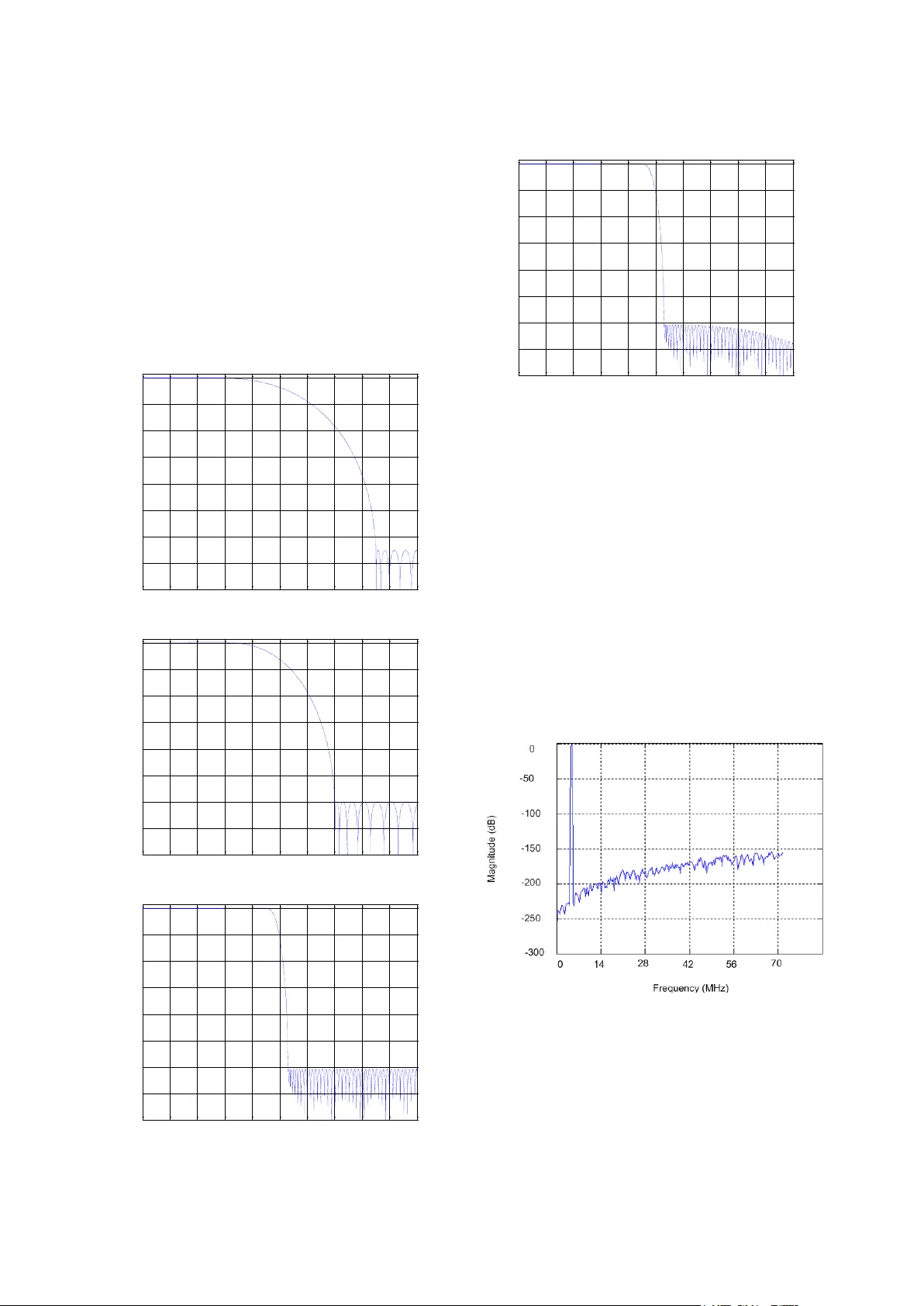
VLSI Implem entation of Cascaded Integrator Comb Filters for DSP Ap plications Rozita Teymourzadeh , Masuri Othman Department of Electrical, Electronic and Systems E ngineering VLSI Design Research Gro up National University o f Malaysia rozita60@vlsi.eng. ukm.my Abstract The recursive comb filters or Cascaded Integrato r Comb filter (CIC ) are commo nly used as d ecimators for the sigma delta modulato rs. This p aper presents the VLSI implementation , analysis and design of h igh speed CIC filters which are b ased on a low-pa ss filter. These filters are used in the signal decimation which has the effect on reducing the samp ling rate. It is also chosen because its a ttractive property of both low power a nd low complexity since it dose n ot required a multiplier. Si mulink toolb ox available in Matlab software which is used to simulator and Verilog HDL codin g h elp to verify the functionality of the CIC filters. Desig n procedures and examples a re given for CIC filter with emphasis on frequency respon se, transfer f unctio n and reg ister width. The implementa tion results sho w using Mod ified Carry Look-ah ead Adder for summation and also apply pipelined filter structure enhan ced h igh spee d and make it more compa tible for DSP applica tion s. Keyword: CIC, sigma delta, Decimation, Comb, recursive, truncation , MCLA. 1 Introduction Electronic and communication system for speech processing and r adar make use of sigma delta modulator in t heir operation [1] , [2]. Future systems are required to operate with high speed and therefo re the sigma delta modulator must be desi gned accord ingly. Sigma delta (∑Δ) modulator is an over sampled modulation technique whic h provides high resolution sample output in contrast to the standard Nyquist sampling technique. However at the output, the sa mpling process is needed in ord er to bring do wn the high sa mpling frequenc y a nd ob tain high re solution . T he CIC filter i s a pr eferred tech nique for th is purpose. In 1981, Eug ene Ho genauer [3] invented a new cla ss of economical digital filter f or decimation called a Cascaded Integrator Comb filter (CIC) or recursive comb filter. Additio nally the CIC f ilter d oes not require storage for filter coe fficients and multipliers a s all coefficients are unity [4]. Furthermore its on -chip implementation i s ef ficient b ecause of it s regular structure consisting of two basic building blocks, minimum e xternal co ntrol a nd less complicated local timing is required a nd its change factor s is reconfigurable with the additi on of a sca ling cir cuit a nd minimal changes to the filter timing. It is also used to perform filtering of the o ut of band quantizatio n noise and prevent excess alia sing i ntroduced during sa mpling rate decrea sing. Hence enhanced high speed w ill be key issue in chip implementatio n of CIC d ecimators. This filter co nsists of three par ts which are Integrator, comb and do wn sampler. CIC filter is co nsidered as rec ursive filter because of the feedbac k loop in integrator circuit. The next section describes t he mathematical formulation and block diagram of CIC filters in detail . Enhanced high speed architect ure is expl ained in sectio n 3 . Sectio n 4 shows implementation and design result in brief. Finally conclusion is expr essed in section 5. 2 An overview of deci mation system The purpose of the CIC filter is t wofold; fir stl y to remove filtering noise which could be aliased back to the base b and si gnals and secondly to con vert high sample rate m-b it data strea m at the output of the Sigma - delta modulator to n-bit data strea m with lower sample rate. This pr ocess is also kno wn as dec imation which is essentially perfor ming the averaging and a rate reduction functions simultaneo usly. Figure 1 sho ws the decimation process using CIC filter . Fig . 1 Digital Dec imation Process The t wo half ba nd filters [7 ] are used to reduce re ma in sampling rate reduction to the N yquist output r ate. Firs t half band filter and seco nd half band filter m ake the frequency re sponse more flat and sharp si milar to ideal filter frequency response. Sigma delta modulator CIC filter Second half band filter First half band filter Droop correction 6. 144 MHz 384 KHz 192 KHz 96 KHz 48 KHz Input Signal 2 1 R 16 0 R 2 2 R 2 3 R Droop correction filter is allocated to compensate pass band attenuation w hich is c reated by CIC filter . The frequency respo nse o f overall system will be shown in section 4. 2.1 CIC filters structure The CIC filter co nsist of N stages o f i ntegrator and comb filter which are connected by a down sa mpler stage as sho wn in figure 1 i n z do main. T he CIC filter has the following transfer function: 1 0 1 ) ( ) 1 ( ) 1 ( ) ( ). ( ) ( RM k N k N N RM N C N I z z z z H z H z H (1) where N is t he number of stage, M is t he differential delay and R is the deci mation factor. In this pap er, N, M a nd R ha ve been chosen to be 5, 1 and 16 respectivel y to avoid overflow in each stage s. R 1 1 1 z RM z 1 S F R F S decimator Comb Integrator Input sample rate Output sample rate Fig. 2 One- stage of CIC filter block diagram N, M and R are parameters to determine the register length requirements necessary to as sure no data loss. Equation (1) can be expr ess as follow: From t he equation, the maxi mum re gister growth/widt h, m a x G can be expressed as: N RM G m ax (3) In other word, m ax G is the maximum re gister growth and a function of the ma ximum output magnitude due to the worst possible i nput conditions [3]. If the input data word length is in B , most significant b it (MSB) at the filter outp ut, m ax B is given by: ] 1 l og [ 2 m a x in B R N B (4) In ord er to reduce the data lo ss, nor mally the first stage of the CIC filter has maximum n umber of bit co mpared to the other stages. Si nce the integrator stage works at the highest oversampling rate with a large i nternal word length, decimation ratio and filter order increase wh ich result in more po wer consumption and speed li mitation. 2.2 Truncation for low power & high speed purpose Truncation means estimating and re moving Least Significant B it ( LSB) to red uce the area require ments o n chip and power consu mption and also increase spee d o f calculation. Although this esti mation and removing introduces additional er ror, the error c an be made small enough to be acceptab le for DSP app lications. Figure 2 illustrates five sta ges of the CIC f ilter whe n m ax B is 25 bit so truncation is ap plied to red uce register width. Matlab software helps to find word length in integrator and co mb section. 1 Z + + + - Integrator 1 25 bit 1 Z + + Integrator 2 22 bit R 1 Z + + Integrator 3 20 bit 1 Z + + Integrator 4 18 bit 1 Z + + Integrator 5 16 bit 16 1 Z Comb 1 16 bit + - 1 Z Comb 2 16 bit + - 1 Z Comb 3 16 bit + - 1 Z Comb 4 16 bit + - 1 Z Comb 5 16 bit a_in s_out Fig. 3 Five-stages of truncated CIC filt er include inte grator and comb cell 3 Speed Improve ment There are two ways to speed up the CIC filter which describes as belo w. 3 .1 P ipeline structure One way to have hig h speed CIC filter is b y implementing the pipeline filter str ucture. Figure 4 shows pipeli ne CIC filter structure when truncation is also applied. In the pip elined structure, no additio nal pipeline registers are used . So that hardware r equirement is the same as in the non-pipeline [6]. CIC d ecimation filter clock rate is deter mined by the first integrator sta ge that ca uses more prop agation delay than any other stage due to maxi mum nu mber o f bit. So it is p ossibl e to use a higher cloc k rate for a CIC deci mation filter if a pipeli ne structure is used in the integrato r stages, as co mpared to non-pipelined integrator stages. Clock rate in integrator N N RM k N RM k k N RM k k N RM k k N RM k k RM z z z z k h z H 1 0 1 0 1 0 1 0 ) 1 ( 0 1 ) ( ) ( (2) section is R times hi gher than in the comb section, so pipeline structure can not applied for co mb section. 1 Z R 1 Z 1 Z 1 Z 1 Z 1 Z 1 Z 1 Z 1 Z 1 Z + + + - + + + + + + + + + - + - + - + - 25 bit 22 bit 20 bit 18 bit 16 bit 16 in Comb 1 16 bit Comb 2 16 bit Comb 3 16 bit Comb 4 16 bit Comb 5 16 bit out Integrator 1 Integrator 2 Integrator 3 Integrator 4 Integrator 5 Fig. 4 Five- stage of trun cated pipeline CIC filter include integrator and comb cell 3.2 Modified Carr y look-ahead Adder (MCLA) The other technique to i ncrease speed is using Modified Carr y Look-ahead Adder. T he Carry Look - ahead adder (CLA) is the fastest ad der w hich can be used for speedin g up p urpose b ut the disadva ntage of t he CLA adder is that the carry logic is getti ng quite complicated for more tha n 4 b its so Modified Carry Look-ahead Adder (MCL A) is introduced to replace as adder. This improve i n sp eed is due to the car ry calculation in MCLA. In the ripple carry adder, m ost significant bit addition ha s to wait for the carr y to ripple through from the least signi ficant bit additio n. T herefore the carry of MCLA add er has beco me a focus of study in speeding up the adder circuits [5]. The 8 bit MCLA structure is shown in Figur e 6. Its b lock diagram consists o f 2, 4-bit module which is connected and each previous 4 bit calculate s carry out for the next carry. T he CIC filter in this paper has five MCLA in integrator parts. The maximum numbe r of bit is 25 and it is decreased in next stages. So it truncated respectively to 25, 22, 20, 1 8 and 16 bit in each adder, left t o right Notice that eac h 4-bit add er pro vides a group P ropagate and Generate Signal, which is used by the M CLA Logic block. T he group Propagate P G and Generate G G of a 4 - bit adder will have the following expressio ns: 0 1 2 3 . . . p p p p P G (5) 0 1 2 3 1 2 3 2 3 3 . . . . . . g p p p g p p g p g G G (6) The most i mportant eq uations to ob tain car ry o f each stage have been defi ned as belo w: ) . ( 0 0 0 1 c p g c ( 7) ) . . ( ) . ( 0 0 1 0 1 1 2 c p p g p g c ( 8) ) . . ( ) . . ( ) . ( 0 . 0 1 2 0 1 2 1 2 2 3 c p p p g p p g p g c ( 9) ) . . . ( ) . . ( ) . ( 0 1 2 3 1 2 3 2 3 3 4 g p p p g p p g p g c ) . . . . ( 0 0 1 2 3 c p p p p Calculation of MCL A is based on above equations. 8 -Bit MCLA Adder could be co nstructed co ntinuing along i n the same logic p attern, with the MSB carr y-out resultin g from OR & AND gates. The Verilog code has been written to implement summation. T he MC LA Veri log code was d ownloaded to the Xilinx FPGA chip. It was found minimum clock period on FPGA board is 4.389ns (Maximum Freq uency is 22 0 MHz). a0 b0 p0 g0 a1 b1 p1 g1 a2 b2 p2 c1 c2 a3 b3 p3 g3 CLL-1 c3 a5 b5 p5 g5 a6 b6 p6 g6 c6 a7 b7 p7 g7 c7 a4 b4 p4 g4 c4 c5 CLL-2 c8 c4 s0 s1 s2 g2 s3 PFA PFA PFA s5 s6 s7 s4 PFA PFA PFA PFA Fig. 5 The 8 bit MCLA structure 4 Design Results Figure 6 ill ustrate th e f requency response of the CIC filter when the sampling frequency is 6.144 MHz a nd the pass band frequency is 34 8 KHz. 0 1 2 3 4 5 6 7 x 10 5 -1 60 -1 40 -1 20 -1 00 -8 0 -6 0 -4 0 -2 0 0 SIN C Filter Freq ue ncy (H z) Amplit ude( dB ) Fig. 6 Comb filter frequency response for R=16, M=1 and N=5 (10) After the sigma delta modulator, the sa mpling rate must be reduced to 47 KHz w hich is the Nyquist sa mpl ing rate. T his is ca rried out in 4 -stages. T he first stage involves the red uction of the sampling freque ncy by the decimation factor of 16. This is done by the CIC filter . The remaining 3 stages involve the red uction of t he sampling freq uency b y the decimation factor of 2 o nly which are carried o ut b y the f irst half band, d roop correction and the second h alf band respectivel y. The Simulation results for all 4 stages are given in figure 7. 0 0.2 0.4 0.6 0.8 1 1.2 1.4 1.6 1.8 2 x 10 5 -1 60 -1 40 -1 20 -1 00 -8 0 -6 0 -4 0 -2 0 0 First Half -b an d Filt er Freq ue ncy (Hz) Amplit ude( dB ) 0 1 2 3 4 5 6 7 8 9 10 x 10 4 -1 60 -1 40 -1 20 -1 00 -8 0 -6 0 -4 0 -2 0 0 Dr oo p Cor rect ion Filt er Freq ue ncy (Hz) Amplit ude( dB ) 0 0.5 1 1.5 2 2.5 3 3.5 4 4 .5 5 x 10 4 -1 60 -1 40 -1 20 -1 00 -8 0 -6 0 -4 0 -2 0 0 Second Half -ban d Filt er Freq ue ncy (Hz) Amplit ude( dB ) 0 5 10 15 20 25 30 35 40 45 50 -1 60 -1 40 -1 20 -1 00 -8 0 -6 0 -4 0 -2 0 0 Ov er al Sy s tem Freq ue ncy (kHz ) Amplit ude( dB ) Fig. 7 frequen cy respo nse of (a) first ha lf ba nd filter (b) droop correction (c) second half band filter (d) ove ral l decimation p rocess , Over sampling ratio=128 Figure 8 shows t he measured b aseband o utput spectra before ( Figure 8(a)) and after ( Figure 8(b)) the decimation functions. The CIC f ilter Verilog code was wr itt en an d simulated by Matlab software. It is found Sig nal to Noise ra tio (SNR) is 141. 56 dB in sigma delta modulator o utput and SNR is increased to 145.35 dB in the deci mation stages. To improve the signal to noise rati o, word length of recursive CIC filter should be increased but the speed of filter calculation is also d ecreased. (a) (a ) (b ) (c ) (d) ( b) Fig. 8 S ignal spectra (a ) Out put sigma delta modulator SNR (b) Output C IC filter SNR 5 Conclusions Recursive CIC filters have been designed and investigated. Enhanced high Speed CIC filters was obtained by the pipeline structure and by using the modified carry look -ahead ad der (MCLA). The evaluation indicates that the pipelined CIC filter with MCLA adder is attractive due to high speed when both the d ecimation ratio and filter order ar e no t high a s stated in the Hogenauer Comb filter. Since the first stage of CIC filter req uire maximum word length and also b ecause of the rec ursive loop in its structure, thus power is limited by the calculation in inte grator stage , so the tru ncation will r educed the po wer consumptio n to obtain high speed operatio n. References [1] R.E.Crochiere and L. R. Rabiner, Multirate Digita l Signal Pro cessing , Enge lwood Cliffs, Prentice Hall, New Jersey, 1983 . [2] P.P. Vaid yanathan, Multirate Systems a nd Filter Banks , Engelwood Cliff s, Prentice Hall, New Jersey, 1993. [3] E.B. Hogenauer, An Eco nomical Class o f di gital filters for Decimation and interpolation, IEEE Transactions on Acoustics, Speech, and Signal Prosessing , Vol. ASSP -29,pp .155-162, April 198 1. [4] Sangil P ark, Principles of Sigma- delta Modulation for A nalog- to -Digital Converters , Motorola Inc, APR8/D Rev.1, 19 90 [5] Michael D. Ciletti, Advance d Digital d esign with the V erilog HDL , P rentice Hall, Dep artment of Electrical and Computer E ngineering U niversity o f Colorado at Co lorado Springs, 2 003 [6] Y. Dj adi and T. A. K wasniewski, C. Chan and V. Szwarc, “A h igh throughput Programmable Decimation a nd I nterpolation Filter ” , Proceedin g of Internationa l Conference on Signal Processing Applications and Technology , pp.1743-1748, 1994 [7] Brian P. Brandt and B ruce A. Wooley, A Low - Power, Area -Efficient Dig ital Filter for Decimation and Interpolation, IEEE Journal of So lid-State Circuits, Vol. 2 9, No.6, June 1994
Original Paper
Loading high-quality paper...
Comments & Academic Discussion
Loading comments...
Leave a Comment