I2C Management Based on IPbus
CBM (Compressed Baryonic Matter) is mainly used to study QCD phase diagram of strong interactions in high and moderate temperature region. Before the next generation GBTx based CBM DAQ system is built up, the DPB (Data Processing Board) layer is used…
Authors: Shiyu Luo, Junfeng Yang, Kezhu Song
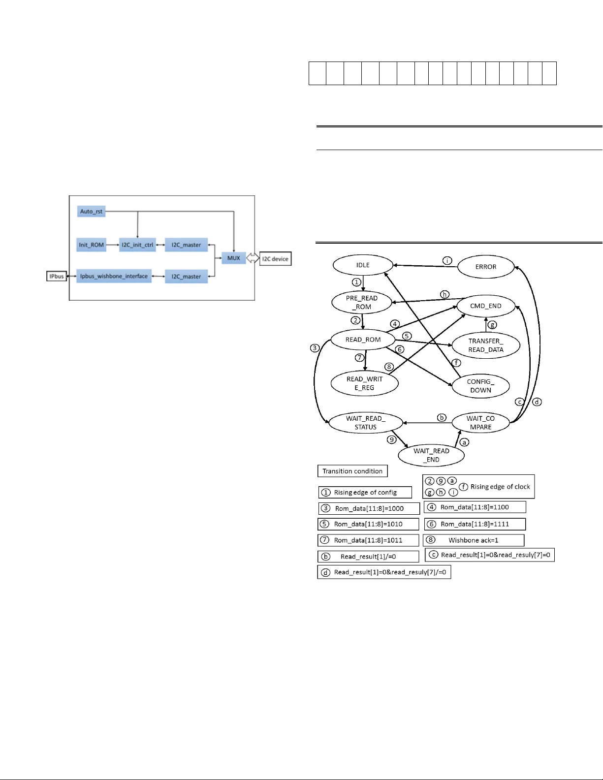
Abstract — CBM (Compressed Baryonic M atter) is mainly used to study QCD phase diag ram of strong interactions in high and m odera te temperature region. Before the next generation GBTx based CBM DAQ syste m is built up, the DPB (Data Proce ssing Board) layer is used in da ta readout and data pre- processing, where a general FPGA F MC carrier board nam ed AFCK is used. T his paper m ainly describes the manage m e nt of the Inter-inte grated Circuit (I2C) dev ices on AF CK and the FM Cs it carr ies via IPBus, an FPGA-based slow control bus used in CBM DAQ system. On AFCK, the connection o f IPBus depends on the correct initialization of a set of I2C devices, including the I2C-bus multiplexer (choosi ng correct I2C bus), the clock crosspoint switch (providing the 125MH z needed by 1000BASE-X/S GMII), the serial EEPROM with a EUI- 48 address (providing t he AFCK M AC address). An independent initial module ca n execute an I2C co mm and sequence stored in a ROM , through w hich the FPGA c an write t o/read from the I2C devices witho ut IPBus, so that the related I2C devices are correctly initialized and the necessary preparatio n for t he IPB us start-up is fulfilled. After the initialization, a Wishbone I2C master core is used as an IPbus slave and all other I2C devices can be configured directly via IPBus . All the design has been fully tested in the CBM DPB design. Index Terms — IPbus, I2C, MMC. I. I NTRODUCTI ON The Compressed Bar y onic M atter (CBM) experiment is one of the experiments at the Facility for Antipro ton and Ion Research (FAIR) in Dar mstadt. The CBM expe riment are composed of k inds of dete ctors, including Micro Vertex Detector (MVD), Silicon Tracking System (STS), Muon Chamber (MUCH), Ring I maging Chere nkov Detector (RIC H), Transition Rad iation Detector (TRD),T im e of Flight Detect or (TOF), and Projec tile Spec t ator Detector (PSD). All these detectors are equipped with the appr opriate Front End Electronics (FEE) boards and Readout B oards (ROB) w hich are located near to the detec tors in the irradiated area. Before the next generation GBTx based CBM DAQ system is built up, the data from the FEE and ROB are injected into a separate intermediate layer named DP B layer, where more complex functionalities, such as slow control, time The authors are w i th the Sta te Key Laboratory of Particle De tection and El ectronics, Univer sity of Science and Te chnology of China, Hef ei 230026, Chi na and also withDepartme nt of Modern Phy si cs, Univer sity of Science and Te synchronization, data readout, data pre-process and data for mat converting, are implemented. I n current C BM DAQ architecture, all these function s will be i m plemented in a Field Programmable Gate Array ( FPGA). Consider ing the o ptimal balance between the cost and performance, a versatile FPGA - based platform, the AMC FMC Carrier Kintex (AFCK) is u sed in kinds of the DPB p rojects to support different detectors. AFCK is a versatile proto type for high-speed co ntrol and data processing applicatio ns, which supp orts the extension boards connected via two HP C FMC con nectors. On AFCK, a set of I2 C devices can be configured fro m the Mod ule Management Controller ( MMC) software or fro m t he FPG A, including: (a) I2 C bus multiplexer: Select different I2C buses co ntrolled by FPGA or MMC; (b) Clock crosspoint switch: Confi gu re the interc onnection of the clocks in AFCK; (c) Programm able Clock generator : Generate local clock, with White Rabbit (W R) function supported; (d) I2C serial EEPROM with a E UI-48 address: Store the unique board I D, wh ich can be used as Ethernet MAC address; (e) System Mo nitor ICs: M onitor th e system status w ith temperature, voltage and c urrent sensors; (f) Other I2C devices, esp ecially the I2C devices on FMCs. Fig. 1. I2C conne ction diagram Although these I2C devices can be configured via MMC when power up, it is important for DAQ system that all these I2C devices can be on-line configured via the slow control bus. In CBM DAQ, the slo w con trol is based on IP Bus ([ 2]), an open-source FPGA core which controls a Wishbone -like b us via Ethernet w ith full y dedicated soft w are packa ge ( c++ or Python). But the setti ngs of IPBus depends on the co rrect configuration of related I2C devices, i ncluding the I2C -bus multiplexer (choosing correct I 2C bus), the clock crosspoint switch (providing the 125MHz need ed by 1000BASE - chnology of China, Hefei 230026,China(e mail: luoshiy u @mail.us tc.edu.cn;sk z@ustc.edu.cn ;yangjf@ustc.e du.cn). I2C Management Based on IPbus Shiyu Luo, Junfeng Yang, Kezhu Song , Hongwei Yu, Tengfei Che n, Tianbo Xu , Cheng Tang X/SGMII), the serial EEPROM with a EUI -48 address (providing the AFCK MAC add ress), which must be con figured before the IPBus can be used. Hence a stand -alone, FP GA- based, programmable I2C configuration mod ule is needed to implement the basic I2C initializatio n when power-up. After t he IPBus link i s setup, a n IPBus I2 C slave will fulfill the contro l needs for all the I 2C d evices connected. All these t w o p arts consist the I2C manage ment m odule for CBM DPB lay ers. II. IP B US _ I 2 C _ CTRL MODUL E D I AGRAM The full architecture of the I2 C m anagement module can be shown as belo w . Fig. 2 . I 2 C connectio n diagram As s hown in Figure 2, there are two I2C controller in the module, one is for I2C device initiali zation, the other is for the in -system operation on I2C device via IPbus. There is an automatical reset sub m odule, in which the reset signal will b e asserted when power-up. This reset s ignal will tri gger the I 2C device initialization m o dule, in which a set of I2C configuration command stored in a ROM can be read out one by o ne and be sent to the appo inted I2C buses. After the I2C device initialization is finished, the I 2C controller switches to the IPbus-based I2C controller automatically. The I2C contro ller in ipb us_i2c_ctrl co re is an I2C master with WI SHBONE interface, so it can be easily either ac cessed directly or connected to IPbus. A set of u se-de fined i2C configuration commands ar e us ed in the I2C device initialization. T hese commands should be saved in a ROM and be read out one by one by the I2C d evice initialization module. At the same time, the i2C device initialization module supports the input and output po rt for complex I2C configuration. III. I 2 C _ I N IT _ CTRL MODULE The in itialization module is used to initialize I2 C device. The initialized control m odule reads out the commands stored in the ROM and used to co ntrols t he I2C device. E ach co mmand stored in t he ROM is 16-bit. The initialization co ntrol module reads out the command by a finite state machine (FSM) . The structure of the co mmand stored in the ROM is s hown in the figure below. The 15th to 13th bits in dicate which i2c bus to be selected. The 12th bit controls the read or write of the i2 c bus. When the level is low, the read oper ation is p erformed. When the level is high, the w rite operation is performed. The 11th bit to the 8th bit represent the register por t. T he corresponding functions of the register are sho wn in Table 1. The remaining 8 bits are written to the I2C cont rol register data. 1 5 1 4 1 3 1 2 1 1 1 0 9 8 7 6 5 4 3 2 1 0 | i2c bus num | | R /W| | register port | | data | Fig. 3 . Comma nd format Fig. 4. Initializ e module state transition diagram The initializatio n co ntroller module is controlled b y a state machine. The state m ac hine consists of a total of 11 states. The command is read in the initial ization module ROM. When the 11th bit o f the instru ction is logic 0, the state of the s tate machine will be transferred from READ_ROM to READ_WRIT E_REG, and then to CMD_END. According to the register port part of t he co mm a nd, the co rresponding register in t he I2C core is read or written . The state transition diagram is shown i n Figure 2. W hen the 11th bit of the command is log ical one, different o perations are per formed according to the register p ort po rtion of the command. The TABLE I F UNCTION OF INITIALIZING MODU LE REGISTER Register port I2C master reg ister Register port Private reg ister 0000 PRERlo(R/W) 1000 CR(W)/SR(R) 0001 PRERhi(R/W) 10 01 Wait read end 0010 Control(R/W) 1010 Transfer read data to output port 0011 TXR(W)/RXR(R) 1011 Write T XR register from input port 0100 CR(W)/SR(R) 1111 Config done specific op erations are shown in T able 1. T he initialization module ha s an external output port and an input port. The data which is r ead by the I2 C device can be sent to t he output p ort and the data from the input po rt can be sent to the i2c device. IV. I 2 C _ MASTER MODUL E After the initialization module co mpletes the i nitialization, i2c master with WISHB ONE inter face directly connected to IPbus. T he I2c m aster has four 8-bit w ide r egisters, which a re control register, transmit/rece ive regi ster, command/status register and two clock pr escale register. When IP BUS is connected to the I2C m aster, IPbus controls i2c device by reading or writing these r egisters. The control register is u sed to enable the I2C core. The transmit/receive register is used to store the tr ansmitted and received data, and th e co mm and/status register is used to stor e the c ommand and status information. The prescale register is us ed to prescal the SCL clock line. The I2C controller reads or writes these registers through the WISHBONE interface. The in itialization m odule directl y co ntrols the i2c device through the WISHBONE b us after po w er up. When the I2C device is required to read or write, the initializatio n module firstly w ri tes the address o f the I2C de vice to the transmit register. And then the I2 C device is strob e. Secondly the address of the device 's register is written to the tra nsmit register. When the i nitialization module w an ts to read th e strobe register , it only needs to send a read command and wait for the data to be trans m itted to the I2C master through the I2C bus. Then the received data can be read from the receive register through the WISHBONE bus. Then the re ading of the I2C d evice is done. When the register of the strobed device needs to be written, the data on ly needs to be w ritten into the transmission register, then waiting for the r esponse signal to arr ive, and the data is transmitted. V. S OFTWARE AN D ROM COMMAND FIL E PROG R AMMING Before initialization, the progr amm able cr ystal oscillato r is not co nnected to the FP GA. So the initialization module needs a separate clock to drive it. A fter initialization, the system clock will connect to FPGA, and the IPBUS control m odule is driven by the system clock. The initialization module read s command fro m the ROM to control the I2C device. The initialization module first configures the SCL clo ck li ne so that the I2C bus can transmit data normally. Seco ndly t he initialization co ntrol module enables the I2C bus th rough the control register. Then the initialization m odule controls t he I 2C master to strobe the clock crosspoint switch, which is m ainly used to configure the interconnection o f the clo cks. The initialization module controls 1 25MHz clock from the crystal oscillator to input to the FPGA's system c lock input port and to the clock input ports of the fo ur high-speed ser ial transceivers throug h the Clock crosspoint switch. When the high-speed serial transceiver has a reference clock, data can be received and transmitted thro ugh the fiber channel. Because the fiber channel is con nected to the high-speed serial transceiver. T hen initialize the control m o dule through the I2C master strobe EEPROM. T he initializatio n module reads t he MAC add ress from the EEP ROM and sends the MAC address to the IPBUS module through the output port of the initialization control m odule. When the high-speed serial transceiver is connected to the fiber channel, the I2C aster can b e directly controlled by the IPBUS. After the initializatio n module is co m pleted, the I2C controller s witches to the I Pbus-based I2C controller. The IPbus-based I2C controller module uses Ether net with fully dedicated software package to control WISHBONE bus. And I2C master is directl y connected to WISHBONE bus. So that we can co ntrol the I2C de vice by so ftware programming directly. The module is u sed to configure P rogrammable Crystal, I2C bus multiplexer, clock crosspoint s witch and programmable crystal on the FMC. Firstly the module needs to initialize the I2C master. T he module ca n set t he operating frequency o f the SCL and enab le the I2C bus. T hen the IPbus - based I2C controller module selects the I2C bus multiplexer. The programmable cr ystal on the AFCK carr ier board is strobed through the I2C bus multiplexer. And t he module w ould set its frequency to 156 .25MHz. Then the clock fr om the programmable crystal oscillator is connected to the clock input port of the high -speed serial transceiver t hrough the clock crosspoint switch, a nd t he high- speed serial transcei ver implements data transmission according to the reference clock. VI. C ONCLUSION The initializatio n control module ca n complete the configuration of so me I2C d evices. However, so m e I2C devices need to be configured in r eal time, so it is necessary to use IPbus to co nfigu re I 2C devices online. The I2 C device can establish connection with IP bus o nly after the initialization is co m pleted. Therefore, the configuration of the I2 C device o n t he AFCK board can be co m p leted onl y whe n two configuration modules are used together. R EFERENCES [1] Robert Frazier,Gr eg Iles,Dave Newbold,A n drew Rose. Software and firmware for controlling CMS trig ger and readout hardware via gigabit Ethernet[J]. Phy sic s Pro cedia,2012, 37. [2 ] M. B odlak ,V. Fr olov,V. Jary ,S. Huber,I . Konoro v,D. Levit,J. Nov y,R. Salac,M. Viri u s. Development of new d ata acquisition system for COMPASS experime nt[J]. Nuclear an d Particle Phy sics Procee dings,2016,273-275. [3] G habrous L arrea C, Harder K, Newbol d D, e t al. I Pbu s: a f lexible Ethernet- based control sy st e m for xTCA hardware[J]. Journal of Instrumentation, 20 15, 10(2):C02019-C0 2019. [4] Z hang Y, He L, Xu Z, et al. A sy stem ve rification environment for mixed- signal SOC desig n based on I P bus[J]. 2003, 1.
Original Paper
Loading high-quality paper...
Comments & Academic Discussion
Loading comments...
Leave a Comment