Noise Measurements of High-Speed, Light-Emitting GaN Resonant-Tunneling Diodes
We report here the first RF noise measurements on two designs of n-doped GaN/AlN double-barrier resonant tunneling diodes (RTDs), each having a room-temperature negative differential resistance (NDR) and also strong near-UV light emission. The measur…
Authors: E. R. Brown, W-D. Zhang, T. A. Growden
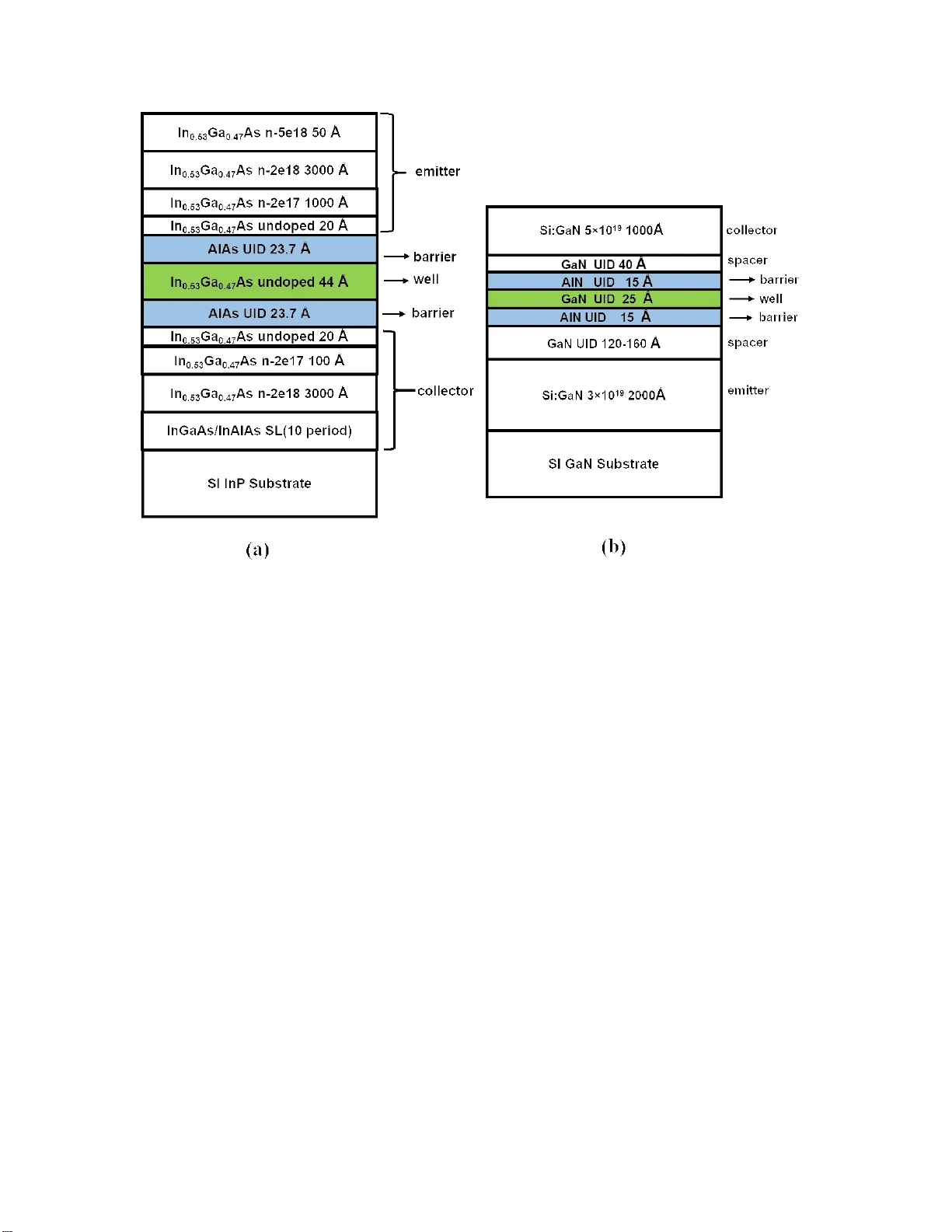
Noise Measuremen ts of High-Sp eed, Ligh t-Emitting GaN Resonan t-T unneling Dio des E. R. Bro wn ∗ and W-D. Zhang † Dep artment of Physics, Wright State U n iv., Dayton, OH 45435 T. A. Gro wden and P . R. Berger Dep artment of Ele ctric al and Com puter Engine ering, Ohio State U niv ., Columb us, OH 43210 R. Dro o pa d Ingr am Scho ol of Engin e ering, T exas Stat e Univ., San Mar c os, TX 78666 D. F. Storm and D. J. Mey er Ele ctr onics Scienc e and T e ch. Division, Co de 6852, U.S. Naval R ese ar ch L ab or atory, Washington, D C 20375 (Dated: June 26, 2018) Abstract W e rep ort here the first RF noise measuremen ts on tw o designs of n -d op ed GaN/AlN double- barrier resonant tunn eling dio d es (R TDs), eac h ha ving a r o om-temp erature negativ e differen tial resistance (NDR) and also strong n ear-UV ligh t emission. The measurements are made with a standard, un-isolated RF receiv er and calibration is made using a su bstitution-resistor/hot-cold radiometric tec hnique whic h wo r k s in the p ositiv e differen tial resistance (PDR) region but not th e NDR r egion. A high-quality InGaAs/AlAs d ouble-barrier R TD is used as a cont r ol sample and displa ys shot noise supp ression down to Γ ≈ 0.5 in the PDR region, as exp ected. The GaN/AlN R TDs d ispla y b oth shot-noise enhancement and su ppression in the PDR r egions, but no obvious sign o f sudden shot-noi s e enhancemen t in the thresh old bias r egion of ligh t emission. This sup p orts the hyp othesis that the holes required for ligh t emiss ion are created by electronic (Zener) in terband tunneling, n ot impact ionization. F urther the minimum sh ot-noise factor of Γ ∼ 0.34 suggests that the GaN/AlN R T Ds are acting lik e triple-barrier devices. ∗ Email: elliott.brown@wright.edu † Email: wzzhang @fastmail.fm 1 I. INTR O DUCTION Thirt y ye a rs ago, the double-barrier resonant-tunneling dio de (R TD ) w a s one of the most studied solid-state devices in the w orld. Displa ying a ro om-temp erat ure negativ e differen tial resistance (NDR) and quan tum-limited (tunneling) transp ort , the R TD offered a very high maxim um frequency of oscillation > 1.0 THz [1] and 2.0-ps-gra de switc hing sp eed. [2] This led to a n um b er of in teresting applications including a lo cal oscillator in mm-w av e-to-THz hetero dyne receiv ers [3] and fast switc hes in triggering circuits, [4] to name a few. Although the sp eed of the R TD in these a pplicatio ns was impressiv ely fast, in terest w aned b ecause of the longstanding problem of dc instability of R TDs in in tegrated circuits without isolation. In r ecen t y ears, this problem has b een mitiga ted b y the monolithic integration of R TDs in sp ecial circuits, suc h as R TD oscillators coupled to resonan t an tennas. [5, 6] In the oscillator and other a pplications, a recurring question is the noise c ha racteristics of R TD-based circuits b ecause t wo-terminal devices , in general, do not provide input-output isolation. In t his pap er, w e rep o rt the first measuremen ts o f the noise b eha vior made on the latest v ersion of R TDs those fabricated from the wurtzite GaN/AlN materials system with o nly n- t yp e doping on freestanding GaN substrates. A recen t univ ersit y-led basic researc h effort has resulted in AlN double-barrier R TDs ha ving stable and high-sp eed ND R,[7, 8] similar to that dev elop ed fo r GaAs/AlAs in the 1980s. [9] But it has tak en man y y ears t o reach this p o in t b ecause the GaN/AlN heterostructures bring greater difficult y in t he design, MBE gro wth, and fabrication. This is largely b ecause of the strong piezo electric effects that o ccur at the heteroin terfaces and sp o n taneous pola rization that is inheren t to the wurtzite structures. [10] The design r ules for successful GaAs/AlAs R TDs do not work fo r GaN/AlN devices without sp ecial care in solving P oissons equation for the band b ending in the presence of the h uge p olarization fields ( ∼ 5 × 10 6 V/cm). In addition, the MBE grow th (pla sma assisted) is c hallenging, a s is the dry etc hing of micron-scale devices. [11] As an added b enefit, these GaN/AlN R TDs hav e displa y ed pronounced ligh t-emission effects not previously rep orted in GaAs/AlGaAs or similar unip o lar-n-dop ed materials. [12] The strongest emission ( ∼ 360 nm) has o ccurred in the near-UV just ab ov e the GaN bandgap, suggesting that a significan t density of free holes is created somewhere in the device structure. Tw o p ossibilities for the hole generation ar e Zener (interband) tunneling a nd cross-gap impact ionization. Both are m ediated b y the large in ternal electric fields in the dev ices and are difficult to discriminate from I-V measuremen ts alone. Ho w eve r, impact ionization 2 alw ay s en ta ils a n enhancemen t of the current noise compared to normal (i.e., full) shot noise assuming the m ult iplicatio n gain M is >> 1. [13 ] This is routinely the case in impact ionization av alanche tr a nsit-time (IMP A TT) dio des, [14] and av ala nc he photo dio des. [15]A second reason for studying the noise b ehav ior is that GaAs- and InP-based R TDs ha ve long displa y ed in teresting mo dification of the shot noise with suppression in the PDR regions and, when measure ment is feasible, enhancemen t in the NDR region. So, an in teresting question is whether or not GaN/AlN R TDs display a similar b ehav io r . And these are in addition to the widely-held b elief that noise can rev eal a sp ects of the device ph ysics no t seen in the time-a ve r a ged transp o rt parameters, and sub ject to a famous quote. [16] I I. EXPERIMENT S AND RESUL TS The measureme nt of noise in R TDs is a non- trivial exercise in circuit coupling, stabilit y , and calibratio n. Past measuremen ts of GaAs- or InGaAs-based devices ha v e b een made with some type of circuit isolation. Lo w RF measuremen ts (t ypically b elo w 1 MHz) hav e b een made with the coupling to high-impedance v oltag e amplifiers , and on R TDs ha ving v ery lo w p eak- current-dens ity ( J P ) so that the differen tial conduc ta nce G w as low enough to obtain dc-bias stabilit y was ac hiev ed in t he NDR regio n without oscillation. [17 – 19] Higher frequency measuremen ts ( typically 1 GHz and ab ov e) hav e b een made with coupling to standard 50-ohm circuits but con taining a micro w av e circulator [20] or isolator [21] b et wee n the R TD and the first amplifier. Both metho ds ha v e displa y ed suppression of the shot noise in the PDR regio ns as re presen t ed by the generalized shot noise pow er sp ectral densit y , S I = 2 eI 0 Γ, where e is the electron c ha r ge, I 0 is the a ve ra ge (dc) curren t, and Γ is the shot-noise factor ( < 1.0 for suppression). Shot noise enhancemen t (Γ > 1.0 ) has also b een observ ed in the ND R region but only in the low- J P devices [15] or in devices oscillating with high-enough sp ectral purity to estimate Γ f r o m the frequency noise.[17] The presen t metho d is based on the un-isolated RF receiv er circuit sho wn in Fig. 1 . The unpac k ag ed R TD is lo cated on the platen o f a prob e statio n and contacted with 40- GHz ground-signal-gro und prob es. Bias v oltage is applied through a wideband bia s tee and the RF p ort of the bias tee is connecte d to a first-stag e LNA through a 0.75 -m-long coaxial cable. Th e LNA is f o llo we d b y more amplifiers and then tw o filters: (1) a high-Q bandpass filter cen tered at 10 0 MHz, a nd (2) a lo w-pass filter to blo ck RF p ow er ab ov e 15 0 MHz. The 100 MHz cen ter frequency w as c hosen to b e w ell ab ov e the 1 / f noise of the R TDs and other 3 FIG. 1. Blo ck d iagram of exp erimen tal set-up f or measurin g RF noise and near-UV electrolumi- nescence simulta n eously . Th e DUT is the GaN/AlN R TD device under test. comp onen ts in Fig . 1, but well b elow the frequency where they b ecome reactiv e through their inte r na l capacitance. The output of the filters is f ed in to a logarithmic p o we r detector ha ving an op erating ra nge b etw een ∼ -60 and -3 0 dBm. The equiv alen t noise bandwidth (ENBW) of the amplifier-chain plus filters was 3.7 MHz. The output of the p ow er detector w as connected to a signal a ve r a ging DC v oltmeter, and the R TD under t est w as biased with a Keithley 240 0 set in voltage-source mo de. Meanwhile , the light emission from the R TD w as monito red with a sensitiv e Si photo dio de coupled optically to the device with a brass ligh t pip e. T he photo dio de curren t w as measured with an electrometer (accurate do wn to ∼ 1 pA). Calibration of the receiv er w as carr ied out b y a substitution-resistor, hot- cold (SRHC) metho d. A set of metal- film resistors spanning the range of 10 to 4.7 k w ere connected directly to coaxial lines in shielded b o xes. Eac h w as connected directly to the bias tee of Fig. 1 and the output p ow er w as measured b oth at ro om temperature ( ∼ 295 K) and at 77 K, the latter measureme nt made p ossible b y immersing the resistor b o x in liquid nitro gen. High-qualit y metal film resistors are kno wn to hav e lo w inductance and s mall c hange in resistance (t ypically 2%) b et we en ∼ 295 and 7 7 K. By the Y- factor metho d, [22] w e deriv ed the ga in and noise temp erature o f the receiv er in the narrow 100- MHz-cen tered passband as a function of source resistance. T hen with the R TD device in place, the receiv er con tr ibutio n to the total noise p o w er subtracted out, leav ing just the noise contribution f rom the R TD. Finally , the R TD noise w a s analyzed with an equiv alen t circuit mo del for the R TD mo deled as a differential conductance G in shun t with the shot noise curren t generato r and in series with a con tact resistance. This mo del ignores devic e capacitance, whic h is generally negligible at 100 MHz in the R TDs tested here. The t hermal-noise con t ribution of the con tact resistance 4 FIG. 2. Stru ctures of R TDs: (a)InGaAs/AlAs, and (b)GaN/A lN. Th e un it for doping den sities is cm − 3 . w as found to b e similarly negligible. This calibration pro cedure w as not a pplicable to the NDR region b ecause of the lac k of any negative substitution resistor. As a pr o of-of- concept, the calibrat ed receiv er w as first demonstrated on a control sample consisting of an R TD of predictable b eha vior: a high qualit y In 0 . 53 Ga 0 . 47 As/AlAs R TD [Fig. 2(a)] hav ing mo derate J P ( ≈ 20 kA/cm 2 ) previously-measured fo r its fast switc hing sp eed. [23] The upw ard- g oing I-V curv e and R TD-sp ecific noise p ow er are plotted in Fig. 3(a), and the differen tia l conductance and shot-noise f actor in Fig. 3(b). The I-V curv e displa ys a p eak- t o -v alley c urrent ratio of PV CR ≈ 12 and a c hair-like b eha vior in the NDR region c haracteristic of a circuit oscillation. The noise-p ow er vs. bias v oltage is monotonic except for a drop out of p ow er in the NDR regio n and p eak just b elow and ab ov e it. T he oscillation in the NDR region is o ccurring a t a frequency we ll ab ov e the 1 00-MHz passband (as observ ed with the spectrum analyzer in Fig. 1), but it is strong enough to satura te the amplifier c hain and decrease the noise p o wer in the passband accordingly . The p eak in p ow er j ust b elo w the ND R is asso ciated with the r apidly increasing curren t (and shot noise ) , whereas the p eak ab o ve it is attributed mostly to the lo w differen tial conductance around the v a lley 5 FIG. 3. Exp erimen tal r esu lts for h igh qualit y InGaAs/AlAs R TD at room temp er atur e and plotte d vs bias vol tage: (a) Electrical current (left axis), and noise p o wer (righ t axis). (b) Differen tial conductance (left axis), and shot-noise factor (right axis). p oint. E very where else in the PDR bias regions the shot noise is readily analyzed, and the shot-noise factor plotted in Fig. 3 ( b). As exp ected f rom all previous studies o f GaAs- and InGaAs-based double-barrier R TDs, the shot noise is suppresse d (Γ < 1.0) in the PDR regions with a minim um Γ ≈ 0.5. A t a bia s j ust b elow 0.4 and ab ov e 1.1 V are not attr ibuted to any intrinsic noise effect but rather to p oin ts where the receiv er gain reac hed a maxim um asso ciated with the imp edance matc h b etw een the R TD and LNA. W e then connected a mo derate- J P ( ≈ 2.7 × 10 3 A/cm 2 ) GaN/AlN double-barrier R TD [Fig. 2(b)][7] through a G SG prob e, and monitored the light emission [inset of Fig. 4 (a)]. The resulting I-V, L- V and noise p ow er curv es are plotted in Fig. 4(a) where the bias v oltage was k ept b elo w 6.2 V to a void device burn-out. T he NDR region o ccurs b et w een 6 FIG. 4. Exp erimental results for mo derate curr en t densit y GaN/AlN R TD at ro om temp eratur e and plotted vs bias volta ge: (a) Electrica l current and photo curr en t (left axis), and n oise p o wer (righ t axis); (b) Differen tial condu ctance (left axis) and shot noise factor (righ t axis). The ins et in (a) sh o ws the R TD device-under-test emitting violet light (long-w av elength tail of sp ectrum cen tered in the near-UV). ∼ 3.8 and 4.2 V and display s a PV CR of ≈ 1 .08 along with the c hair-like structure indicative of oscillations. The threshold fo r strong ligh t emission o ccurs a t ∼ 4.8 V. The no ise p ow er is similar to the InGaAs R TD displa ying pronounced p eaks adja cent to the NDR re g ion and also the oscillation-induced drop-out in the ND R regio n. But w ell aw ay f rom the NDR region, the b eha vior is more complicated as evidence d by the ob vious p eak in noise p ow er around 5.2 V. This corresp onds t o an inflection p oint in the G-vs-V curv e in Fig. 4(b), and after the noise analysis o ccurs in a region where the shot noise factor is decreasing to < 0.4 . There is no sign of a sudden increase in the shot noise near the ∼ 4.8 V threshold of ligh t 7 FIG. 5. E x p eriment al r esults for high-current-densit y GaN/AlN R TD at ro om temp erature and plotted vs bias volta ge: (a ) Electrical curr en t and p h oto current (left axis), and noise p ow er (r igh t axis), (b) Differentia l condu ctance (left axis), and shot noise factor (r igh t axis). emission, whic h suggests that the mobile holes required for the cross-gap ar e created by a normal-shot-noise mech a nism, suc h as Zener tunneling, no t impact ionization. Interes ting ly , at bias v oltages w ell b elow the NDR region (e.g. ∼ 3 V), the shot noise is enhanced (Γ > 1.0) for reasons that are not y et understo o d. Finally , w e connected a high- J P ( ≈ 2.0 × 10 5 A/cm 2 ) GaN/AlN double-bar r ier R TD in the same manner as ab o ve . [24] The resulting I-V, L-V and no ise p ow er curv es are plotted in Fig. 5(a ) where the bias v oltage w as k ept b elo w 7.3 V to a v o id device burn-out. The NDR regions o ccurs b et w een ∼ 6.5 and 7.0 V a nd displa ys a PVC R o f ≈ 1.26 along with the chair-lik e structure indicative of osc illa tions. The threshold for strong light emission o ccurs at ∼ 6.5 V in the midst of the NDR region. T he noise p o wer is similar qualitative ly to the mo derate- J P GaN/AlN R TD but is larg er in magnitude, consisten t with the higher 8 curren t and shot noise of this device. A t low bias v oltages, the shot noise is enhanced to o (for example ∼ 2.1V). The p eaks adjacen t to the NDR region are also less prominen t, consisten t with a close r impedance matc h to the LNA, but the noise in the ND R region drops out once again. At a giv en bias v oltage the light emission is w eake r than in the mo derate- J P device, and displa ys a more abrupt threshold. But this migh t b e an a rtifact of its coincidence with t he ND R region or due to the structure difference of the tw o R TDs. [12, 2 0] Another distinction of the high- J P device is the b eha vior b elo w the current p eak. The high- J P device sho ws its gr eatest degree of shot-noise suppression [Fig . 5(b)] at ≈ 6.0 V with Γ ≈ 0.34. Figure 5(a) also sho ws an ob vious lo cal p eak in the noise p ow er a round 3.0 V, and 5 (b) a lo cal c hair at the same bias. As describ ed in a separate manus cript, this is attributable to electron tunneling through the low est quasib ound state E 1 of the GaN R TD, meaning that the primary p eak at 6.4 V is lik ely electron tunneling through E 2 . [2 5] I I I. SUMMAR Y In conclusion, w e ha ve p erfor med the first-known measureme nts of the noise behavior of GaN/AlN R TDs and related it to the electrical (I-V) and light-emission (L-V) c haracteristics. W e observ e no definitiv e sign of noise enhancemen t at the lig h t-emission threshold, consisten t with the required hole generation b eing by Zener tunneling, not impact ionization. On the other hand, the shot noise do es display substan tial suppression in the PDR regions of the device abov e the NDR region in the low J P device, and b elow it in the high J P device. The shot-noise factor of ∼ 0.34 is b elo w the double-barrier (F ano) limit of 0.5, but close to the triple-barrier limit of 0.3 3. [26] GaN/ AlN R TDs are kno wn to ha ve deep pre-w ells ( ∼ 0.5- 0.7 eV) on the emitter side of the structure and a high pre-barrier ( ∼ 0.1-0.2 eV) separating t he AlN barriers from the quasi-neutral region on the emitter side. If true, t his w ould suggest that the GaN/AlN devices studied here are acting lik e triple-barrier devices a result made p ossible b y noise measuremen ts and mo deling. This w ork was sp o nsored b y a MURI Progra m (DA TE) under Dr. P aul Maki a nd the U.S. Office of Na v al Researc h. The first author ac kno wledges Dr . P atric k F a y of Notre Dame Univ ersit y for helpful commen ts ab out noise measuremen ts. [1] E. R. Br own et al., App l. Phys. Lett. 58 , 2291 (1991). 9 [2] J. F. Whitak er, G. A. Mourou, T . C. L. G. S ollner, and W. D. Go o dh u e, Ap pl. Phys. Lett. 53 , 385 (1988). [3] R. Blun dell, D.C. Pa p a, E .R. Br own, and C.D. Park er, Electronics Lett. 29 , 288 (1993). [4] S. K. Diamond et. al. App l. Phys. Lett. 52 , 2163 (1989). [5] M. Asada, S. Suzuki, and N. K ishimoto, Jp n. J. Appl. Phys. textbf47, 4375 (2008). [6] M. F eigino v, C. S ydlo, O. C o jo cari, and P . Meissner, Appl. Ph ys. Lett. 99 , 23350 6 (2011). [7] T. A. Gr owden et al., Ap pl. Phys. Lett. 109 , 08350 4 (2016). [8] J. E ncomendero et al., Phys. Rev. X 7 , 0410 17 (2017). [9] M. Tsu c hiya, H. Sak aki an d J. Y oshino, J ap . J. Appl. Phys. 24 , No. 6 (1985). [10] O. Am b ac her et al., J. Ap p l. Phys. 85 , 3222 (1999). [11] D. F. S torm et al., J. V ac. Sci. T ec h. B, 35 , 02B110 (2017). [12] T. A. Gro wd en et al., Nature Ligh t: S cience & App lications acc epted article preview 27 Octob er 2017; doi: 10.1038/lsa .2017.150 [13] R. J. McInt yr e, I E EE T rans on Electron Dev. 13 , 164 (196 6). [14] M. E., Hin es, IEEE T r ans. Electron Dev. 13 , 158 (1966). [15] P . Y u an, et al., IEEE T rans Electron Dev. 46 , 1632 (199 9). [16] ’Go d lo ves the noise as m uch as the signal., Lewis M. Branscom b [17] Y. P . Li et al., Phys. Rev. B 41 , 838 8 (1990). [18] G. Iannaccone, G. Lom bardi, M. Macucci, and B. Pelleg r in i, Ph ys . Rev. Lett. 80 , 1054 (19 98). [19] V.V. Ku znetso v, E.E. Mendez, J.D. Bruno, an d J.T. Pham, Ph ys . Rev. B 58 , R10159 (1998). [20] E.R. Bro w n, C.D. P ark er, A.R. Cala w a, and M.J. Manfra, IEEE T rans. Electron Devices, 38 , 2716 (1991). [21] A. Przadk a et al., Appl. Ph ys . Lett. 71 , 530 (1997) . [22] F undamental s of RF and Micro wa ve Noise Figur e Measurement s Applicatio n Note, Keysigh t T ec hn ologies, www .k eysight .com/find /nf [23] T. A. Growden, et al., App l. Ph ys . Lett 107 , 153506 (2015). [24] T. A. Growden et al., App l. Phys. Lett., acce p ted Dec. 201720 17. [25] V. Po u y et and E. R Brown. IEEE T r ans. on Electron Dev. 50 , 1063 (2003). [26] A. K. M. New az et al., Phys. Rev. B 71 , 1953 03 (200 5). 10
Original Paper
Loading high-quality paper...
Comments & Academic Discussion
Loading comments...
Leave a Comment