Design of 32-channel TDC Based on Single FPGA for {mu}SR Spectrometer at CSNS
Muon Spin Rotation, Relaxation and Resonance ({\mu}SR) technology has an irreplaceable role in studying the microstructure and properties of materials, especially micro-magnetic properties. An experimental muon source is being built in China Spallati…
Authors: Fanshui Deng, Hao Liang, Bangjiao Ye
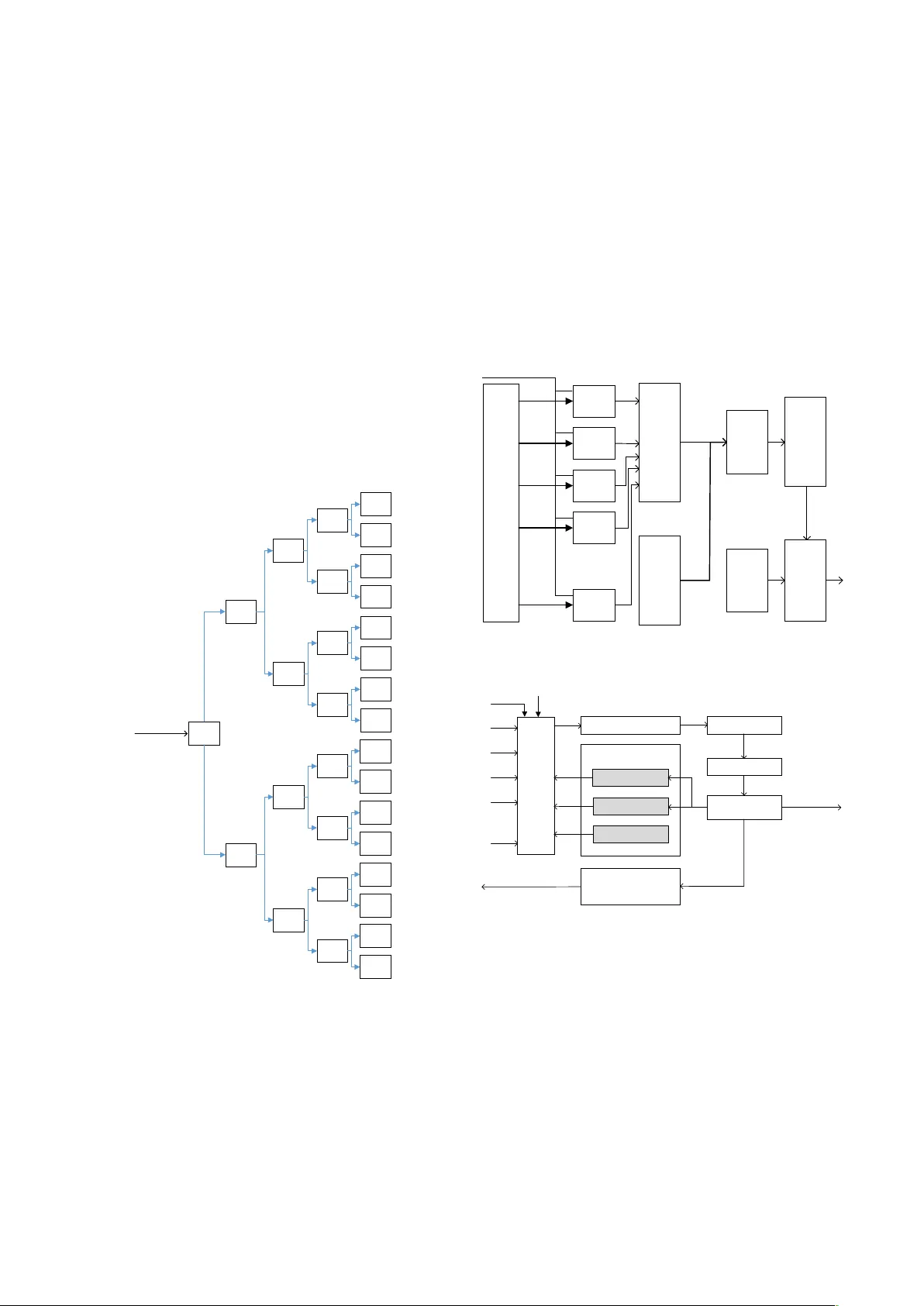
Abstract —Muon Spin Rotation, Relaxation and Resonance (uSR) technology has an i rreplaceable role in studying the microstructure and properties of materials, especia lly micro- magnetic pro perties. An exp erimental muon source is being built in China Spalla tion Neutron Source (CSNS) now . At the same time , a 128-channel uSR spec trometer as China's first uSR spectrometer is being developed. Th e time sp ectrum of uS R can be o btained by fitting the curv e of positron count rate with time. This paper presents a 3 2-channel Time-to-Digital Co nverter (TDC) implemented in a Xilinx Virtex-6 Field Programmable G ate Arr ay (FPGA) fo r measuring the positron’s flight time of μSR Spectrometer. Signal of each chann el is sampled by 16 equidistant shifted-phase 200 MHz sampling clocks, so the TDC bi n size is 312.5ps. The measuring range is up to 327us. This TDC has t he ability to store multipl e hit signals in a short time with a deep hit- buffer up to 512. Time tag is add ed to each data to record the moment w hen the data was detec ted. Programmable tim e window and cha nnel shielding give t he f lexibility to cho ose the ti me rang e and channels of interest. The delay of each channel can be calibrated. The da ta is transmitted to data acquisition syste m (DAQ) throu gh Gigabit Ethernet . TDC a nd control lo gic ar e configured in real time by DAQ. The results of te st sho w tha t the Full Width at Half Maximum (FWHM) prec i sion of single channel is better than 27 3 ps with a low sensitivity to temperature and the linearity is pretty well. Index Term s —TDC, shifted clock sampling, FPGA, μSR, CSNS. I. I NTRODUC T ION HE use of mu on's spin properties to study the properties of materials is called Muon Spin Rotation, Relaxatio n and Resonance ( SR) technology. SR techn ology has an irreplaceable role in stu dying the microstruct ure and properties of materials, especially micro-magne tic properties . Currently only ISIS in t he UK , J-PARC i n Japan, PSI i n Switzerl and and TRIUMF in Canada have high-perf ormance muon sources fo r SR appli cations. An experim en tal muon so urce i s bei ng built in China Spallat ion Neutron S ource (CSNS) n ow [1] , [2]. At the same time, a 128-channel SR spectr ometer as China's fi rst SR spect rometer is being develo ped. Manuscript received June 15, 2018 . This work was sup por ted by the National Na tural Sci enc e Foundation o f China under G r ants 115278 11 . F. S. Deng is with the State Ke y Laboratory of Particle Detectio n and Electronics, University of Science a nd Te chnology of China ( USTC), Hefei 230026, China (e -m a il: dfsh@mail. us tc.edu.cn). H. L iang is with the State K e y Labo ra tory of Pa rticle Detection and Electronics, University of Science a nd Te chnology of China ( USTC), Hefei 230026, China (e-m a il: simo n lh@ustc.edu.cn). This SR spect rometer uses a double ring structure with 64 det ectors placed in f ront of and behind th e sampl e. The moment th at muon b eam enters the sampl e chamber serves as a start si gnal, and th e moment that the detector ar ound the sample det ects positrons generated by muon deca y ser ves as a stop si gnal. Muon's lif etime can be obtain ed by measuri ng the positron's flight ti me. The time spectru m of SR can be obtained b y fittin g th e curve of positron c o unt ra t e w i th t ime and then can reveal the internal physical stru cture o f the sample in formation. So the measurement of positron’s flight tim e is the key t o the entire SR spect romet er. In o rder to measure the positron’s flight t ime, a 32-channel Time-to-Digit al Con verter (TDC) is implemented in a Xilinx Virtex-6 Field Programmabl e Gate Array (FPGA). II. DESIGN AND IMP LEMENTATION A. Desi gn Method TDC desi gn bas ed on FPGA h as t wo main methods [3]. The one i s dela yed d ata sampli ng (DDS), the in put signal i s routed to a number of delay units connected in serie s , and each de l ayed si gnal is s ampled by the flip-flop using a common clock. The other one is shifted-phase clock sampling (SCS), the input si gnal is s ampled with flip-flops using a set of equidi stant shifted -phase sampling clo ck. So far, high-precision TDC has been implement ed i n a single FPGA u sing dedicated carry chains [4]. But the price i s th e consum ption of a large number of logical res ources. Taking i nto acc ount the pr ecision requirement s in t his project is not hi gh and a great d eal of control l ogic is needed, so this TDC uses the second metho d. Xilinx virtex-6 FPGA has 32 gl obal clock lines but onl y 12 global cl ock lines can be routed in one regi on. In this design, th e external cl ock is multiplied by t wo PLLs to gener ate e ight 200MHz clocks th at h ave th e s ame frequency but a difference of 22.5 degr ees between the two adjacent clocks . Beca use flip- flops in FPGA ca n be con figured to be activated by th e rising edge or falli ng edge of the clock, the in put signal can be routed to 16 flip-flops, with 8 flip -flops being activated b y 8 clock rising edge and the other 8 flip-fl ops being activated by 8 cl ock B. J . Ye is w ith the State Key Laboratory of Pa rticle Detection and Electronics, University of Science and Technology of China (USTC), Hefei 230026, China (e-m ail: bjye@ustc.edu.cn). J. Y . Tan g i s with Institute of Hig h En ergy Ph ysics, C h inese A cad emy of Sciences, Beij ing 100049, China (e-m a il: t ang jy@ihep. ac.cn) . Design of 32-channel TDC Based on Single FPGA for μSR Spectrometer at CSNS Fanshui Deng, Hao Liang, Bangjiao Ye, and Jingyu Tang T falling edge. This is equi valent t o the input signal being sampled by 16 equidistant shift ed-phase 200MHz clocks. The TDC bin size is Tclk/N, where Tclk i s the period of sampling clock, and N is the number of s ampling clo cks. So th e bin size is 5ns/16 =312.5ps. The precision of TDC i s greatly limited b y the linearity of TDC bi ns, and the most significant effect o n the li nearity of TDC bi ns i s the time s kew of input si gnal routing to 16 flip- flops. In order to minimize time s kew, t he LUTs (Look-Up Tables) in FP GA are used as shown in Fi g. 1. Th e input signal is routed to 16 flip-flops afte r four stages of LUTs a n d th es e LUTs are p laced sy mmet ricall y in the same slice colum n [5]. The INIT parameter for the FPGA L UT pri mitive is what gives the LUT its logical value. Set the INIT value to 2’h2, then when the LUT i nput is 0, its out put will be configured t o 0, when t he LUT i nput is 1, its o utput w ill b e confi gured t o 1. Thus the output o f t he LUT will b e equal to the input. Aft er suffi cient area constraints and timing constr aints, the tim e skew can be reduced to a few picoseconds. B. TDC Desig n Fig. 2 is the s chematic of one T DC channel. The input signal is routed to 16 flip-flops drive n by 1 6 shifted-phase clocks w it h minimal tim e skew, th e value of flip -flops i s encod ed int o a 4- bit binary code as a fine cou nt an d then the fine count is s ent to the hit- b uff er with coarse count. The da t a is f inall y sto red in the readout F I FO after pa ssing thr o ugh th e trigger count er. Becaus e th e ti me measurement range is required to reach h undreds o f micros econds, the coarse count er is a 16 -bit co unter d riven by 200MHz c l ock, s o th e ti me meas urement range i s u p to 327us. After the arrival o f th e Muon pulsed beam, the single -channel det ector may recei ve multiple positrons in a s hort time, and th ese signals need to be recorded, so the T DC is designed to be multi -stop and it h as a deep hit-buffer up to 512. T h e tri gger counter can be configured as exter nal t rigger or int ernal s elf- trigger to decide whet her the data is res erved or discarded and to record the number of t rigger si gnals. The time tag w ith second level is used to r ecord th e moment when the hit s ignal is det ected. C. FPGA Impl ementatio n This TDC contains a start channel and 3 2 stop channel s, s o onl y one coar se counter i s needed. Schematic of 32-channel TDC and contr ol l ogic in a single FPGA is shown i n Fig. 3 . 54bit data of each TDC, including 20bit t ime data, 26bit time tag an d 8bit tri gger count , i s packaged i nto 64bi t aft er ch annel coding and then stor ed in th e FIFO, an d fin ally uploaded t o data acquisiti on sy st em (DAQ) through Gigabit E t hernet. Because th e entire sy s tem currentl y h as 128 channels, a 7-bit channel coding is used a s the identificati on number for each channel. TDC's configuration section incl udes channe l shiel ding, time LUT Flip- flop LUT LUT LUT LUT LUT Flip- flop Flip- flop LUT Flip- flop Flip- flop Flip- flop Flip- flop Flip- flop Inp ut signal Flip- flop Flip- flop Flip- flop Flip- flop Flip- flop Flip- flop Flip- flop Flip- flop LUT LUT LUT LUT LUT LUT LUT LUT Fig. 1. Time sk e w is minimized by ins erting LUTs . Fli p- flop Fli p- flop Fli p- flop Fli p- flop Fli p- flop ··· Shifted-phase clocks cl k 0 cl k 1 cl k 2 cl k 3 cl k 15 ··· In p ut signal Encoder Coarse cou nt er Hit-buffer Trig ger cou nter Time tag Readout FIFO Fig. 2. Schem at ic of one TDC cha nnel. 32-channel TDC ··· Channel coding Configuration Data packing FIFO Gigabit ethernet MAC IP core Self-checking and D A C Threshold control Channel shielding Time window Error detectio n Start Stop[1] Stop[2] Stop[3] Stop[4] Stop[32] Trig g er To front-end electronics To PC software Fig. 3. Schem at ic of 32-channel TDC and control logi c in a singl e FPGA. window setting an d error detection. Channel shielding an d ti m e window are used t o select the channel a nd time range of int erest to the user. Error detection is use d to reset the entir e TDC l ogic when an error occurs. This FPGA is also responsible for controlling the front-end electroni cs, including the sel f-checking and Digi tal to Analog Converter (DAC) threshold fo r each ch annel. The front-end electroni cs p eriodicall y simulate the detector signals and th e FPGA a lso generates pe r iodic p ulse signals when self-checking. The puls e signal generated by the FPGA is sent to the TDC serves as a start signal and the timing p ulse outp uts by the front - end electronics are also sent to t he TDC serve as stop s ignals. On th e one h and, th e entire el ectronics system can be test ed whether it can work normall y without the detector conn ected, on the oth er han d, the dela y o f each ch annel can be calib rated. TDC and co ntrol logic can be configured in r eal time b y DA Q. III. T EST RESULTS We tested the time measurement performance between t he start channel and one of the stop channels. T he test m ethod is to generate the periodic st art si gnal and stop signal b y the Tektronix AFG3252C dual channel ar bit rary / fun ction generator, st art signal and stop signal are then conn ected to t he TDC, an d the time measur ement results are upload ed to DAQ via Gigabit Ethernet. Test results are shown i n Fig. 4, t he FWHM precisio n is equal to 368.1ps. Change the tim e interval between th e start signal and the stop signal , makin g multipl e meas urements in 200 ps steps. After 27 times measurements, the worst is 3 85.8ps. So th e FWHM precision of single ch annel is b etter th an 385.8/ √ 2 =2 73ps wit h a l ow sensiti vity t o temp erature. The fitting curve of expectation with input time interval is shown in Fig. 5, t he correl ation coefficient R^2 is close to 1.000 0 (0.99999989) , so the linearity is p retty well. IV. C ONCLU S ION In this paper, a 32-channel TDC is implement ed in a single Xilinx Vi rtex-6 FPG A to measu re t he p ositron’s flight time o f μSR Spectrometer at CS N S. T his TDC has the abilit y to store multi ple hit si gnals i n a short t ime and th e meas uring r ange is up to 327us. The FWHM pr ecision is better than 273ps and the linearit y is pretty. R EFERENCES [1] S. N. Fu, H. S. Chen, Y. W. Chen, Y. B. Chen, H. Y. Dong, S. X. Fang, K. X. Huang, W. Kang, J. Li, H. C. L i u, L. Ma, H. F. Ouy ang, H. M. Qu, H. Sun, J. Y. Tan g, C. H. W ang, Q. B. Wang, S. Wang, T. G. Xu, Z. X. Xu, C. Zhang, J. Z han g, ” Status of csns project,” Pr oceedings of the 4t h International Particle Accelerator Conference, pp. 3995-3999, 2013. [2] Y. Chen, H. T . J ing, J . Y Tang,”Physical D es ign of the Superferric Dipol e for EMuS,” IEEE Transactions on Applied Super conductivi t y, vol. 28, Ap r. 2018. [3] M. Büchele, H. Fi sc her, F. Herr mann, K. Königsmann, C. Sch ill, S. Schopferer, ”The GANDALF 128-Channel Time-to- Dig ital Converter,” Physics Procedia, vol. 37, pp. 1827-1834, 2012 . [4] J. Kuan g, Y. G. Wan g, Q . Cao, C. Liu, “ Impl e mentation of a high precision multi-m easur ement tim e -to-digital convertor on a K intex -7 FPGA,” Nuclear Instruments a nd M ethods in Physics Research Section A: Acce l er ators, Spectrometers, Dete ctors and Associ a ted Equi pment, vol. 891, pp . 37-41, 2018. [5] Y. G. Wang, P. Kuang, C. Li u , “A 256-channel m u lti-phase cl ock sampling-b ased time-to- dig ital converter implem ented in a Kintex-7 FPGA,” Confere nce R e cord - IEEE In strum enta tion a nd Measurement Technolo gy Conference, vol. 2016-July , Jul. 2016. Fig. 4. Measured FWHM p rec ision of TD C chann el. Fig. 5. F i tting curve of ex pectation with input tim e interval. 20.255 20.455 20.655 20.855 21.055 21.254 21.455 21.655 21.855 22.055 22.254 22.455 22.655 22.854 23.054 23.254 23.453 23.653 23.853 24.053 24.253 24.453 24.653 24.853 25.054 y = 1.0000 x - 0.1450 R² = 1.0000 19 20 21 22 23 24 25 26 20 21 22 23 24 25 26 Expectation/ns I n put time interval/ns
Original Paper
Loading high-quality paper...
Comments & Academic Discussion
Loading comments...
Leave a Comment