Analysis and Design of 8-Bit CMOS Priority Encoders
A comprehensive review and fair comparison of previous priority encoder (PE) designs over the past one and a half decades are presented using a 45 nm technology. Further, potential limitations of existed PEs are identified, based on which we propose …
Authors: Xiaoyu Wang, Yukang Feng
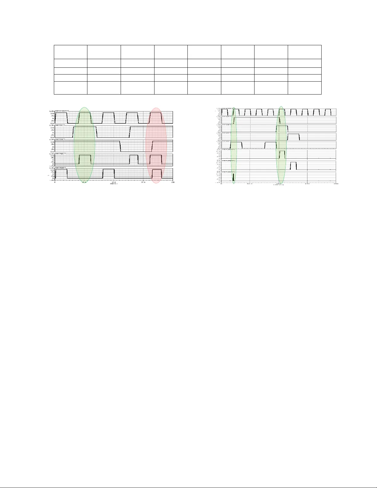
Anal ysis and Design of 8-Bit CMOS Priority Encoder s Xiao yu W ang and Y ukang F eng University of Virginia {xw5ce, yf4rs}@virginia.edu ABSTRA CT A com prehensiv e rev iew and fair c omparison of previous pri- orit y encoder (PE) designs ov er the past one and a half decades are presented using a 45 nm tec hnology . F urther, potential limitat ions of existed PEs are identified, based on whic h we prop ose a robust PE design. The new PE is abl e to eliminate race condition and charge sharing problem which are suffered by almost all the previous designs. Besides, the proposed PE can also b e used in comprising higher order PEs by incorp orating a carefully designed lo ok-ahead struc- ture. Sim ulation results demonstrate that our design can ac hiev e one of the b est p ow er and dela y p erformance among previous PEs and are free from p otential risks. K eywords Priorit y Encoder, F air Comparison, Race Condition, Charge Sharing, Higher Order Priority Encoder 1. INTR ODUCTION A Priorit y enco der (PE) is a basic but critical unit in digital systems, and it has been widely used in many applications, suc h as fixed and floating p oint units, comparators, incre- men ter/decremen ter circ uits, sequen tial address encoder of con ten t addressable memories and so on. In a multi-bit PE, eac h bit is assigned a priority w eighting according to its own position w eigh ting. A logic-1 priorit y tok en is ini tially and temporarily giv en to all bits. While the bit with a higher priorit y accepts a logic-1 input, it will pass a logic-0 signal to update the priorit y tokens of those low er priority bits to disable their priority . Meanwhile, when any one bit accepts a logic-0 input, it will also lose its priorit y by definition. F or eac h input pattern, only the bit keeping the logic-1 token can generate a logic-1 output, while all the other bits will get logic-0 outputs. Since late 1990s, more than eight different PE designs were proposed to achiev e lo w er pow er dissipation, shorter dela y and also less complexit y . Ho w ev er, critical issues lik e pos- sible charge sharing and race condition which migh t lead to fatal breakdo wn w ere rarely addressed. Based on these observ ations, this pap er first presen ts a fair comparison of differen t PEs using the updated 45 nm process tec hnology in order to shed some ligh t on how to c hoose proper PEs in differen t applications. Next, w e identify ma jor limitations for eac h of existing PE and verify our analysis through sim u- lations. F urthermore, a robust PE architecture suitable for serial cascading is prop osed to get rid of potential c harge sharing and race problems and main tain a decent delay and pow er p erformance at the same time. 2. PREVIOUS WORKS AND LIMIT A TIONS A series of PE de signed w ere proposed during the past decade. In this section, a brief review of the history of PE’s adv ance- men t is presented and some limitations neglected before are iden tified. 2.1 Related W orks Delgado-F rias and Ny athi [1] designed a priorit y enco der that p ermits sequen tial passage of priority tok en from the highest priorit y primary inp ut to the lo west priorit y input – the disadv antage of thi s des ign b eing that the sequen tial passage of priority tok en encount ers a delay of O ( n ), where ’n’ represents the total num ber of primary inputs or out- puts. T o alleviate the linear increase in delay , W ang and Huang [7] put forward tw o 8-bit priority enco der designs, comprising tw o 4-bit enco der blo c ks with the pro vision of an internal look ahead signal – one of the designs extensively utilizes pMOS transistors while the other design widely de- plo ys nMOS transistors. Kun et al . [4] came up with the design idea of an 8-bit pri- orit y encoder mo dule, eliminating the need for sub-mo dules and internal lo ok ahead signaling. While Huang et al . [2] proposed a serial cascading arc hitecture to realize higher or- der priority encoders, with the lo ok ahead output of a 8-bit encoder mo dule serving as the lo ok ahead input for the suc- ceeding enco der blo c k, Kun et al . [4] prop osed a parallel priorit y-based cascading topology to implemen t larger size priorit y encoders. Mohanra j et al . [5] presented a new 8-bit priorit y enco der design, which is in fact a refinement of Kun et al .’s enco der design by exploiting shared logic to reduce the num ber of devices needed for physical realization. Huang and Chang [3] in troduced a new NOR- based priorit y encoder, whe re during the prec harge phase of the clock, all the ou tputs a re driv en to logic-high state, and in the ev al- uation phase, based up on input request(s), the input that assumes a higher priority is enabled and its corresponding output is retained as logic high, while the other primary outputs are pulled to logic lo w. In this aspect, the Huang and Chang’s design is similar to Huang et al .’s pMOS-based priorit y enco der design. P anc hal et al . [6] modified Hu ang and Chang’s work and came up with a similar PE based on activ e-lo w logic, which implies tha t input(s) ha v e to be logic lo w so as to activ ate the PE to pro duce a desired logic high output. 2.2 Limitations of Previous W orks The ab o v e describ ed PE designs were prop osed in a time in terv al of more th an one and a half decades, an d thus im- plemen ted using differen t pro cess tec hnologies, including 90 nm, 250 nm and 900 nm, most of whic h are outdated. There- fore, the studied metrics migh t no t be represen tativ e enoug h to reflect their performance disparity . T o the best kno wledge of the authors, there has not b een any thorough and fair comparison of all the ma jor PE designs in the past decade, i.e., utilizing the same up dated pro cess technology . F or this consideration, we implemen t these PEs and measure main design metrics using the same 45 nm pro cess technology , aiming to provide some insights for choosing differen t PEs under different application circumstances. Based on extensive and in-depth study of previous w orks, it is noticed that almost all the designs fo cused on improving the three metrics, i.e., pow er dissipation, worst-case delay and num ber of transistors, which are vital asp ects for PE design. Ho w ever, what they failed to consider is the ro- bustness of these PEs, i.e., whether they could still function correctly in some extreme or unt ypical scenarios. F or in- stance, with some certain input combinations, PEs designed without considering the p ossibilit y of charge sharing prob- lem will generate outputs with low er voltage than logic high or ev en result in flipping. Another example is that due to unexpected delay of the lo ok-ahead signal, a race condition migh t happ en causing the stage losing priority still outputs logic high signal(s). These t w o cases will b oth severely com- promise PE’s robustness and thus limit their applicability or require more complexit y when designing other parts of a system. In addition, since a typical P E only consists of 8-bit inputs and higher order PEs are widely used in v arious sys- tems, the ability of 8-bit PEs to comprise higher order ones though serial cascading is desired in most cases. How ever, some of the previous designs are not suitable for realizing higher order PEs, even though they included a look-ahead signal in their circuits. T able 1 summarizes ma jor limitations of previous PE de- signs in terms of race condition, c harge sharing prob lem and feasibilit y of cascade, in which c hec kmarks represent that corresponding designs suffer from those limitations. F rom T able 1 we notice that all the previous PE designs failed to fix at least one of the problems except the high-sp eed PE proposed in [7], whic h on the hand, has another disadv an- tage that its p ow er dissipation is muc h higher than the rest of PEs. Giv en these observ ations, w e prop ose a robust PE arc hitecture whic h is race-condition and c harge-sharing free, as well as suitable for realizing higher order PEs. 3. PR OPOSED R OBUST PE In a m ulti-bit PE, th e output of the i -th bit is OP i = I P i · P i , where I P i is the corresp onding input data and P i stands for the priority token passed onto this bit. When the input of the low er significan t bit is 0, the priorit y token is p assed onto the next bit, i.e., P i = I P i − 1 · P i − 1 . The general expression of outputs OP i can b e written as O P i = I P i · I P i − 1 · I P i − 1 · I P i − 3 · · · I P 1 · I P 0 (1) F or the proposed 8-bit PE with a three-lev el lo ok-ahead structure sho wn in Fi gure 1, t he fundamen tal equations gov- T able 1: Limitations of differen t PEs Limitations Race condition Charge sharing Unsuitable for cascade W ang and Huang 1 [7] W ang and Huang 2 [7] Kun et al . [4] Huang & Chang [3] (flipping) Mohanra j et al . [5] P anc hal et al . [6] (flipping) erning the PE are giv en as follows O P 0 = LA · I P 0 O P 1 = LA · I P 0 · I P 1 O P 2 = LA · I P 0 · I P 1 · I P 2 O P 3 = LA · I P 0 · I P 1 · I P 2 · I P 3 LA inter = LA + I P 0 + I P 1 + I P 2 + I P 3 O P 4 = LA inter · I P 4 O P 5 = LA inter · I P 4 · I P 5 O P 6 = LA inter · I P 4 · I P 5 · I P 6 O P 7 = LA inter · I P 4 · I P 5 · I P 6 · I P 7 (2) When Clock becomes 0, the circuit is in the pre-disc harge phase. LA inter is 0 and all outputs are pre-discharged to 0. When Clo ck becomes 1, the circuit enters the ev aluation phase. In the circuitry , the p-t ype dynamic gates for O P 0 ∼ O P 3 realize the first-lev el look-ahead functions with la 0 ∼ la 2 acting as the lo ok-ahead signals. Owing to the first-level look-ahead structure, the four outputs O P 0 ∼ O P 3 ev aluate at the same time. LA inter is used to realize the second-level lo ok-ahead func- tion betw een the higher-priorit y and low er-priorit y 4-bit cells and LA is used to realized the third-level look-ahead func- tion to decide whether the current 8-bit macro cell o wns the priority . Note that the new design uses active -lo w lo ok- ahead signals, which means that an other stage with higher w eigh ting o wns t he priorit y when LA is logic 1 . In suc h a case, O P 0 ∼ O P 7 will b e set to logic 0 during the ev aluation phase. If LA is logic 0 to pass the priority into the curren t macro cell, OP 0 ∼ O P 3 are decided by I P 0 ∼ I P 3 directly , while O P 4 ∼ O P 7 are dec ided b y both I P 4 ∼ I P 7 and the second-lev el lo ok-ahead signal LA inter . There are a num b er of adv an tages of the new 8-bit PE cell o ve r the conv entional ones. First, the PE cell is designed to be race-free by using r s 0 ∼ r s 7. At the b eginning of the ev aluation phase, eac h output bit is ev aluated immediately according to the input s ignals and at most one o utput bit will b e charged from 0 to 1. Ho w ev er, these outputs may be incorrect. When the correct lo ok-ahead signal arriv es a IP7 IP0 IP1 IP2 IP3 IP4 IP5 IP6 Clock LA AL_inter OP7 OP5 OP6 OP3 OP4 OP2 OP1 OP0 la0 la2 la1 pd0 pd2 pd1 pd4 pd3 pd5 pd7 pd6 rs7 rs6 rs5 rs3 rs4 rs0 rs1 rs2 Figure 1: Prop osed 8-bit robust priorit y enco der. little bit later than the rising edge of the clo c k signal, if the curren t stage o wns the priorit y both signals LA and LA inter will remain at 0 and the previously ev aluated outputs are exactly correct. Otherwise, if the curren t stage loses it pri- orit y , b oth signals LA and LA inter will be 1 to turn on r s 0 ∼ r s 7 to enforce all the outputs of the curren t stage to be logic low. Second, because the circuit utilizes the three- lev el look-ahead-signal structure, it has t he high-speed char- acteristics. Third, the PE design will not suffer from charge sharing, since there only exist tw o parallel NMOS transis- tors betw een eac h output and groun d. F ourth, due to the series-t ype circuit structure, all outputs will ev aluate in the ev aluation phase but with only one output being charged after the pre-discharge phase and also only the output with high voltage will be discharged in the next pre-disc harge phase. This means a significa nt reduction of the switc hing activit y and the corresp onding switc hing p ow er. Last but not least, given the carefully designed lo ok-ahead signal, the new PE could also be used as a macro cell for comprising higher order PEs by utilizing the parallel priorit y lo ok-ahead arc hitecture of Kun et al . [4]. 4. PERFORMANCE EV ALU A TION AND EX- PERIMENT AL RESUL TS 4.1 F air Perf ormance Comparison of PEs Sev en 8-bit dynamic CMOS PEs including the prop osed de- sign ha v e been implemented at the transistor lev el and sim- ulated us ing Cadence based on a 45nm CMOS process de- Clock LA IP0 IP1 OP0 OP 1 Figure 2: Race condition in the pow er-optimized PE. sign kit from NCSU, i.e., F reePDK, with a supply v oltage of 1.1V. A combination of all the p ossible inputs are applied at a clock frequency of 50 MHz to v erify the functionality of these differen t PEs, as well as to estimate the a v erage pow er dissipation. The total av erage pow er dissipation and critical path delay metrics of differen t 8-bit PEs are giv en in T able 2, along with the device count required for ph ysical design. The device count, in terms of num b er of transistors needed, is assumed to b e representa tiv e of the area o ccupancy of the circuit. F rom T able 2 we notice that the PE presen ted b y W ang and Huang 1 [7] is the fastest design, while its p o w er dis- sipation, PDP and transistor num b er are muc h larger than the rest of the designs, which mak es its m uc h less desir- able in applications. In terms of the four metrics considered here, the p ow er, dela y and area optimized PE prop osed in [5] achiev es the optimal ov erall p erformance, while it comes with the cost of possible race condition and c harge sharing as discussed in Section I I. The prop osed robust PE has a balanced p erformance in these four asp ects, i.e., with a rel- ativ ely small num b er of transistors, th e new PE has one of the smallest pow er consumption, delay and PDP . 4.2 Potential Failur e of Previous PE Designs Giv en the identified potential limitations of previous PE de- signs, in the sectio n, we pro vide some simulation results to confirm our analysis in Section II. F or a PE design failing to consider p otential race condition, i.e., the lo ok-ahead sig- nal that disables the curren t stage arrives after the clock edge starting a ev aluation phase, t he outputs might not b e disabled immediately , leading to unexp ected results. Here the pow er-optimized PE [4] is used as an example and corre- sponding timing diagram is given in Figure 2. F or this design with activ e-high lo ok-ahead sign al, when the lo ok-ahead sig- nal is logic 0, all the outputs of the current stage should be disabled no matter what the input v alues are. How ev er, as sho wn in Figure 2 , when the rising edge of Clo ck arrives, LA is high and the second bit owning the priorit y outputs logic 1, while when LA arrives later, O P 1 w ould not be disabled, leading to the p ossibility that more than one of the outputs ha v e logic 1 in a higher order PE. Next, we consider another fatal problem existing in previ- ous works – charge sharing. In Figure 3, a p ossible output flipping of the p ow er, delay and area optimized PE pro- T able 2: Comparison of Design parameters of different 8-bit dynamic CMOS PEs Design metrics W ang and Huang 1 [7] W ang and Huang 2 [7] Kun et al . [4] Huang & Chang [3] Mohanra j et al . [5] P anc hal et al . [6] New design P ow er ( µ W) 79.11 6.119 9.422 6.544 3.189 7.100 6.879 Dela y (ns) 0.177 0.346 0.292 0.281 0.274 1.018 0.278 PDP (fJ) 14.002 2.117 2.751 1.839 0.874 7.228 1.912 Num ber of transistors 102 103 62 76 55 60 79 Clock LA IP0 IP7 OP0 OP 7 Figure 3: Output flipping due to charge sharing in the pow er, dela y and area opti mized PE. posed in [5] is presen ted. Under normal situations, if the input(s) with higher priority is logic 1, all the outputs of lo w er-priorit y bits should be logic 0, which is shown as in the green circle in Figure 3. Ho w ev er, given some sp ecial com binations of inputs, some outputs will be flipp ed, lead- ing to sev ere malfunction of PEs. The output flipping due to charge sharing is displa y ed with the red ci rcle in Figure 3, where the logic 1 of O P 7 is unexp ected. 4.3 Robustness of the Proposed PE The adv ancement of the proposed PE is mainly reflected in three asp ects, i.e., free of race condition, c harge sharing and the suitability for comprising higher order PEs. The latter t wo adv antages could b e v erified straightforw ard giv en the fact that the outputs are connected to the lo w est part of the circuit and that the third-level lo ok-ahead signal LA is adopted to realize cascading in higher order PEs. Here w e only presen t the sim ulation result in Figure 4 to v alidate the race-condition-free prop ert y of the new PE. Consider the scenario given in the left green circle in Fig- ure 4. At the beginning of the ev aluation phase, the curren t stage owns the priorit y ( LA is logic 0), OP 3 is charged. Then LA arrives later, whic h will disc harge O P 3 immediately , out- putting the correct results. Again, when the current st age c hanges from disabled to enabled due to the arriv al of a logic 0 LA , O P 1 corresponding to the bit which o wns priority will immediately turned to logic 1 without waiting for the next ev aluation phase. Due to careful design of the lo ok-ahead structure, an y potential erroneous arriv al time of the lo ok- ahead signal due to problematic timing design of other parts of a system will be fi xed within the PE, without passing fault outputs to follo wing levels. Clock Active-low LA IP0 IP1 IP2 OP0 OP1 OP 2 Figure 4: Robustness of the proposed PE against race condit ion. 5. CONCLUSIONS A comprehensiv e review of existing PEs and their fair p erfor- mance comparison are presen ted using a 45 nm technology in terms of three design metrics – p ow er, delay and n um ber of transistors. Moreo ver, w e analyze these designs closely to iden tify their p oten tial limitations, including possible race and cha rge sharing problems, and infeasibilit y to compris- ing higher order PEs. Our analysis sho ws that almost all the existing PEs suffer from one or more of these disadv antages. In order to obtain a PE which is capable of o v ercoming these shortages, a robust PE struc ture is proposed, whic h is v al- idated to b e charge-sh aring and race-condition free, prop er for cascading and also hav e one of the best p ow er and dela y performance. 6. REFERENCES [1] J. Delgado-F rias and J. Nyathi. A vlsi high-performance encoder with priority lo ok ahead. In Pr o c e e dings of the 8th Gr e at L akes Symp osium on VLSI, 1998. , pages 59–64. IEEE, F eb. 1998. [2] C.-H. Huang, J.-S. W ang, and Y.-C. Huang. Design of high-performance cmos priority encoders and incremen ter/decremen ters using multilev el lo ok ahead and multilev el folding techniques. IEEE Journal of Solid-State Cir cuits , 37(1):63–76, 2002. [3] S.-W. Huang and Y.-J. Chang. A full parallel priorit y encoder design used in comparator. In Pr oc e e dings of 53th IEEE International Midwest Symp osium on Cir cuits and Systems (MWSCA S) , pages 877–880. IEEE, 2010. [4] C. Kun, S. Quan, and A. Mason. A p o w er-optimized 64-bit priority encoder utilizing parallel priorit y look-ahead. In Pr o c e e dings of the 2004 International Symp osium on Circu its and Systems, 2004. ISCAS’04. , v olume 2, pages I I–753–II–756. IEEE, 2004. [5] J. Mohanra j, P . Balasubramanian, and K. Prasad. P ow er, dela y and area optimized 8-bit cmos priority encoder for embedded applications. In Pr o c e e dings of 10th International Confer enc e on Emb e dde d Systems and Applic ations , pages 111–113, 2012. [6] P . Panc hal, C. Vinitha, R. Sriv asta v a, P . Balasubramanian, and N. Mastorakis. Design of 8-bit dynamic cmos priority resolv ers based on activ e-high and active-lo w logic. Communic ation Systems , pages 82–85, 2013. [7] J.-S. W ang and C.-H. Huang. High-speed and lo w-pow er cmos priorit y enco ders. IEEE Journal of Solid-State Cir cuits , 35(10):1511–1514, 2000.
Original Paper
Loading high-quality paper...
Comments & Academic Discussion
Loading comments...
Leave a Comment