Widlar Current Mirror Design Using BJT-Memristor Circuits
This paper presents a description of basic current mirror (CM), Widlar current mirror, fourth circuit element (memristor) and an analysis of Widlar Configuration with integrated memristor. The analysis has been performed by comparing a modified configuration with a simple circuit of Widlar CM. The focus of analysis were a power dissipation, a Total Harmonic Distortion and a chip-surface. The results has shown that a presence of memristor in the Widlar CM decreases the chip-surface area and the deviation of the signal in the circuit from a fundamental frequency. Although the analysis of power dissipation has also been conducted, there is no definite conclusion about the power losses in the circuit because of the memristor model.
💡 Research Summary
**
The paper investigates the integration of a memristor—a fourth fundamental circuit element—into a Widlar current‑mirror configuration built with bipolar junction transistors (BJTs). It begins with a concise review of the basic BJT current mirror, which uses two matched transistors and a single input resistor to replicate a reference current (Iref = 1 mA) at the output over a wide range of load voltages. The authors then describe the Widlar current mirror, a well‑known variant that adds an emitter‑degeneration resistor to the output transistor, allowing a high input current to generate a much smaller output current without resorting to very large resistors (≥50 kΩ). This is especially valuable in analog integrated‑circuit design where large‑area resistors increase die size and cost.
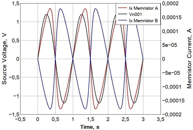
The core contribution is the replacement of the input and output resistors in the Widlar circuit with memristors, modeled using the Joglekar resistance‑switch formulation in LTspice. The memristor’s resistance is a function of the integral of past current or voltage, producing a pinched hysteresis loop in the V‑I plane. The authors simulate the modified circuit and compare its performance against the conventional Widlar mirror.
Power Dissipation:
For the conventional Widlar mirror the authors report average power losses of ~56 mW in the input resistor, ~4.9 mW in the input BJT, ~0.36 µW in the output resistor, and ~128 mW in the output BJT, yielding a total of ~61 mW. In the memristor‑based version the reported losses are ~2.4 mW in the input memristor, ~296 mW in the input BJT, ~0.77 µW in the output memristor, and ~7.16 mW in the output BJT, for a total of ~2.7 mW. The dramatic reduction is attributed to the memristor’s near‑zero static dissipation in the ideal Joglekar model. However, the authors acknowledge that this model omits realistic loss mechanisms (e.g., switching energy, leakage), so the power‑saving claim remains tentative.
Total Harmonic Distortion (THD):
Fourier analysis is performed by driving the circuits with an AC source of the same frequency and measuring the harmonic content of the output current. The conventional Widlar mirror exhibits a THD of 1.94 %, whereas the memristor‑enhanced circuit shows a reduced THD of 1.22 %. The authors interpret this as evidence that the memristor’s hysteretic behavior suppresses higher‑order harmonics, yielding a waveform closer to the fundamental sinusoid.
Chip‑Area Considerations:
The Widlar topology already reduces the need for large resistors, but the memristor’s nanometer‑scale footprint further shrinks the required silicon area. The paper argues that replacing a 50 kΩ–100 kΩ resistor with a memristor can save a substantial portion of the die, which is advantageous for dense analog blocks.
Critical Assessment:
The study provides a clear methodological flow—starting from basic theory, moving through circuit design, and ending with quantitative comparisons. The simulation results are internally consistent, and the use of the Joglekar model is appropriate for a first‑order exploration. Nevertheless, several limitations reduce the impact of the conclusions:
- Model Realism: The Joglekar memristor is idealized; it assumes zero static resistance and neglects temperature‑dependent effects, endurance, and variability. Consequently, the reported power savings may be overly optimistic.
- Parameter Disclosure: The paper does not specify the memristor’s window function parameters, dopant mobility, or switching thresholds, making it difficult to reproduce the results or assess scalability.
- Experimental Validation: No silicon measurements are presented. Real memristive devices often exhibit significant series resistance, non‑linear I‑V characteristics, and stochastic switching, all of which could alter the THD and power figures.
- Statistical Analysis: Only a single set of simulation runs is reported. Monte‑Carlo or corner‑case analyses would be needed to evaluate robustness against process variations.
- Typographical Errors: Some power values (e.g., “128.69W”) appear to be typographical mistakes, which raises concerns about data handling.
Future Directions:
To solidify the claim that memristors improve Widlar mirrors, the authors should fabricate a test chip using a commercially available memristive material (e.g., TiO₂‑based devices) and measure actual power, THD, and area. Additionally, exploring alternative memristor models that incorporate realistic loss mechanisms, as well as performing a sensitivity analysis to process, temperature, and bias variations, would provide a more comprehensive picture.
Conclusion:
The paper successfully demonstrates, via simulation, that integrating an ideal memristor into a Widlar current‑mirror can reduce chip area and harmonic distortion, and potentially lower power consumption. However, the reliance on an idealized memristor model limits the practical relevance of the power‑saving results. Further experimental work and more realistic modeling are required before the approach can be adopted in production analog IC designs.
Comments & Academic Discussion
Loading comments...
Leave a Comment