Electro-mechanical control of an on-chip optical beam splitter containing an embedded quantum emitter
We demonstrate electro-mechanical control of an on-chip GaAs optical beam splitter containing a quantum dot single-photon source. The beam splitter consists of two nanobeam waveguides, which form a directional coupler (DC). The splitting ratio of the DC is controlled by varying the out-of-plane separation of the two waveguides using electro-mechanical actuation. We reversibly tune the beam splitter between an initial state, with emission into both output arms, and a final state with photons emitted into a single output arm. The device represents a compact and scalable tuning approach for use in III-V semiconductor integrated quantum optical circuits.
💡 Research Summary
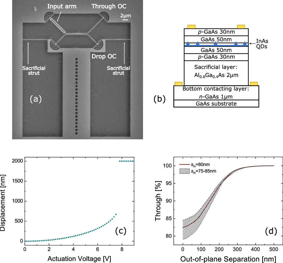
In this work the authors present a fully integrated, electrically actuated, on‑chip optical beam splitter based on a GaAs nanobeam directional coupler (DC) that contains an embedded InGaAs quantum‑dot (QD) single‑photon source. The device consists of two parallel nanobeam waveguides forming a 7 µm long coupling region. One of the waveguides is attached to a 35 µm long, 7.5 µm wide cantilever; the other is rigidly anchored to the substrate. By applying a voltage between the cantilever and a grounded substrate, an electrostatic force pulls the cantilever downward, thereby increasing the out‑of‑plane separation (s_out) between the two waveguides.
Theoretical modeling using MIT Photonic‑Bands (2‑D eigenmode solver) and 3‑D finite‑difference time‑domain (FDTD) simulations predicts that for waveguides 160 nm thick and 280 nm wide with an in‑plane gap (s_in) of 40 nm, the evanescent coupling efficiency remains above 98 % across the 880–980 nm wavelength range. As s_out is varied from 0 to ≈400 nm, the splitting ratio (SR) of the DC can be tuned continuously from an over‑coupled state (≈80:20) to a fully decoupled state (≈100:0).
Experimentally the authors fabricate the structure on a p‑i‑p‑i‑n GaAs membrane that hosts self‑assembled InGaAs QDs in the intrinsic region. After under‑etching the membrane to release the cantilever, the sacrificial struts are removed by low‑temperature laser ablation. Electrical contacts (Ni:Au) to the top p‑layer and the bottom n‑layer enable the application of an actuation voltage (V_act). The cantilever displacement follows a quadratic profile along its length; analytical energy‑minimization predicts a maximum controllable displacement of one‑third the initial gap (s_0≈2 µm), i.e., ≈667 nm, before pull‑in occurs. In practice pull‑in is observed at V_act≈13 V, with a reversible hysteresis loop down to 4 V, indicating sufficient restoring force to overcome adhesion.
Optical characterization is performed at 4.2 K using micro‑photoluminescence (µ‑PL). A single QD emitting at 910.6 nm is resonantly excited via the wetting layer (840 nm CW Ti:sapphire laser). With V_act=0 V the QD emission is detected from both output couplers (through and drop), giving an SR of ≈80:20. When V_act is increased to 12.5 V, the drop output is strongly suppressed while the through output rises, reaching a maximum increase of 17 % relative to the total signal at zero voltage. The authors attribute the non‑monotonic behavior of the drop signal (a peak near 11 V) to interference effects between the moving output coupler and the substrate, which they model with a transfer‑matrix approach.
To link voltage to mechanical displacement, the authors balance electrostatic energy (½ε₀AV²/(s₀−s_out)²) against the cantilever’s spring energy (k s_out). This yields V_act = (s₀−s_out)√(s_out X) with X = √(ε₀A/2k). Using the experimentally observed pull‑in voltage and maximum displacement, they extract X = 2650, allowing conversion of the measured V_act‑dependence of the QD signal into an s_out‑dependence. The resulting curve matches the simulated SR for s_in ≈ 82 nm, confirming that the mechanical actuation reliably tunes the coupling.
Single‑photon purity is verified by an on‑chip Hanbury‑Brown‑Twiss measurement, cross‑correlating photons collected from the two independent paths of the input coupler. The raw second‑order correlation yields g^(2)(0) = 0.25 ± 0.02; after deconvolution with the detector response (FWHM ≈ 874 ps) the corrected value is g^(2)(0) = 0 ± 0.01, confirming near‑perfect antibunching.
The authors discuss the broader impact of their approach. Because the actuation is purely electro‑mechanical, it can be applied to any on‑chip photonic element that requires post‑fabrication tuning, such as routers, phase shifters, or wavelength‑selective switches. Scaling to larger arrays is feasible, and with optimized designs (smaller s_in, longer coupling length, or operation at telecom wavelengths) the device could achieve the standard 50:50 splitting required for many linear‑optics quantum computing protocols while still offering a large tuning range. Predicted switching speeds on the order of 0.5 MHz are within reach using faster voltage drivers.
In summary, this paper demonstrates the first experimental realization of an electrically controlled, out‑of‑plane tunable beam splitter integrated with a quantum‑dot single‑photon source. The work combines rigorous electromagnetic modeling, precise MEMS fabrication, low‑temperature single‑photon spectroscopy, and quantitative mechanical‑electrical analysis to deliver a versatile platform for reconfigurable quantum photonic circuits.
Comments & Academic Discussion
Loading comments...
Leave a Comment