A 6.3pJ/b 30Mbps -30dB SIR-tolerant Broadband Interference-Robust Human Body Communication Transceiver using Time Domain Signal-Interference Separation
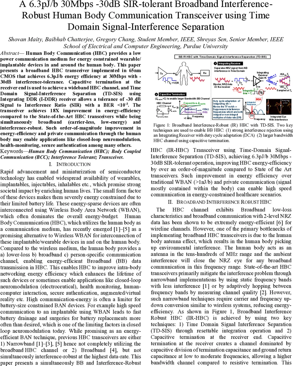
Human Body Communication (HBC) provides a low power communication medium for energy constrained wearable/ implantable devices in and around the human body. This paper presents a broadband HBC transceiver implemented in 65nm CMOS that achieves 6.3pJ/b energy efficiency at 30Mbps with -30dB interference-tolerance. Capacitive termination at the receiver end is used to achieve a wideband HBC channel, and Time Domain Signal-Interference Separation (TD-SIS) using Integrating DDR (I-DDR) receiver allows a tolerance of -30 dB Signal to Interference Ratio (SIR) with a BER <10-3. The transceiver achieves 18X improvement in energy-efficiency compared to the State-of-the-Art HBC transceivers while being simultaneously broadband (carrier-less, low-energy) and interference-robust. Such order-of-magnitude improvement in energy-efficiency and private communication through the human body may enable applications like closed-loop neuromodulation, health-monitoring, secure authentication among many others.
💡 Research Summary
The paper presents a novel human‑body‑communication (HBC) transceiver implemented in 65 nm CMOS that simultaneously achieves ultra‑low energy consumption, broadband operation, and strong interference robustness. By terminating the receiver with a capacitive load, the authors exploit the capacitive division between the body and ground return paths, thereby extending the usable bandwidth compared with conventional resistive termination. The core of the design is a Time‑Domain Signal‑Interference Separation (TD‑SIS) technique realized with an Integrating Dual‑Data‑Rate (I‑DDR) receiver. In TD‑SIS, the incoming waveform—comprising NRZ data superimposed with narrow‑band sinusoidal interference—is integrated over a carefully chosen time window. When the integration window matches the data bit period, any interference whose frequency is an integer multiple of the data rate integrates to zero, while the data integrates to a non‑zero value, effectively nulling the interference. For interference frequencies that are not integer multiples, the duty cycle of the integration clock is adaptively adjusted so that the integration time becomes an integer multiple of the interference period, achieving the same cancellation effect.
The I‑DDR receiver contains two complementary integration‑sampling paths that operate on opposite phases of a 16‑phase clock, enabling true dual‑data‑rate operation without inter‑symbol interference. Each path consists of a reset‑able differential NMOS integrator with P‑MOS switches as the load, followed by a regenerative feedback sampler. A 5‑bit current DAC controls the integrator gain and the sampler offset, allowing the circuit to be tuned across data rates. A Mueller‑Muller CDR extracts timing from two error‑detecting samplers, while a dedicated Interference Period Detector (IPD) measures the on‑time of the interference by converting it to a square wave, discharging a reference capacitor, and comparing the resulting voltage to that generated by the clock. The IPD output feeds a Duty‑Cycle Adaptation (DCA) block that dynamically modifies the integration clock’s duty cycle via an OR gate, ensuring optimal interference rejection.
Fabricated on a 65 nm process with a 0.12 mm² active area, the transceiver was wire‑bonded on a PCB for measurement. Bit‑error‑rate (BER) tests using PRBS data showed that at 30 Mbps the device tolerates a signal‑to‑interference ratio (SIR) as low as –30 dB while maintaining BER < 10⁻³. Energy consumption was measured at 6.3 pJ per bit, representing an 18‑fold improvement over the state‑of‑the‑art HBC transceivers. BER bathtub curves confirm that with DCA enabled, the receiver achieves error rates below 10⁻⁴ even when the interference frequency (e.g., 60 MHz) is not an integer multiple of the data rate. An image‑transfer demonstration over the body channel yielded a peak‑signal‑to‑noise ratio (PSNR) exceeding 50 dB, validating the practical data‑integrity of the system.
In summary, the authors combine capacitive termination with a dynamically adaptive TD‑SIS receiver to deliver a broadband, carrier‑less HBC transceiver that operates at 30 Mbps, consumes only 6.3 pJ/bit, and remains functional under –30 dB SIR. This order‑of‑magnitude energy efficiency gain, together with inherent privacy (signal confined to the body) and robustness to ambient electromagnetic noise, opens the door for high‑speed, low‑power applications such as closed‑loop neuromodulation, continuous health monitoring, and secure body‑centric authentication in wearable and implantable medical devices.
Comments & Academic Discussion
Loading comments...
Leave a Comment