D3NOC: Dynamic Data-Driven Network On Chip in Photonic Electronic Hybrids
In this paper, we present a reconfigurable hybrid Photonic-Plasmonic Network-on-Chip (NoC) based on the Dynamic Data Driven Application System (DDDAS) paradigm. In DDDAS computations and measurements form a dynamic closed feedback loop in which they tune one another in response to changes in the environment. Our proposed system enables dynamic augmentation of a base electrical mesh topology with an optical express bus during the run-time. In addition, the measurement process itself adjusts to the environment. In order to achieve lower latencies, lower dynamic power, and higher throughput, we take advantage of a Configurable Hybrid Photonic Plasmonic Interconnect (CHyPPI) for our reconfigurable connections. We evaluate the performance and power of our system against kernels from NAS Parallel Benchmark (NPB) in addition to some synthetically generated traffic. In comparison to a 16x16 base electrical mesh, D3NOC shows up to 89% latency and 67% dynamic power net improvements beyond overhead-corrected performance. It should be noted that the design-space of NoC reconfiguration is vast and the goal of this study is not design-space exploration. Our goal is to show the potentials of adaptive dynamic measurements when coupled with other reconfiguration techniques in the NoC context.
💡 Research Summary
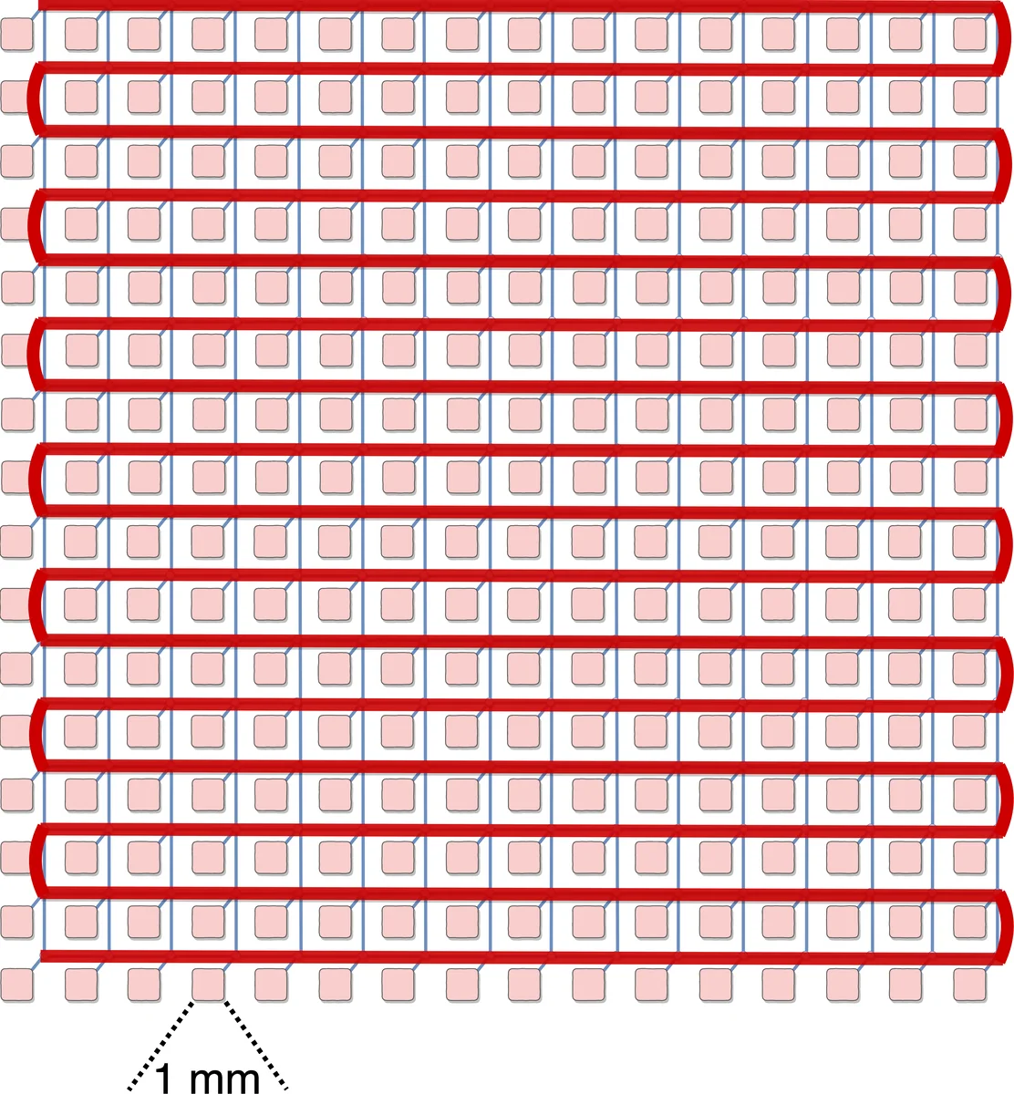
The paper introduces D3NOC, a dynamically reconfigurable hybrid photonic‑plasmonic Network‑on‑Chip that applies the Dynamic Data‑Driven Application System (DDDAS) paradigm to NoC design. Traditional NoCs use static topologies that cannot adapt to changing traffic patterns, leading to under‑utilization, higher latency, and increased power consumption. D3NOC addresses these issues by (1) augmenting a 16 × 16 electrical mesh with a serpentine optical express bus that can be allocated at runtime to a pair of cores with the highest communication volume, and (2) dynamically adjusting the measurement window that governs how often reconfiguration occurs.
The optical interconnect is based on a Configurable Hybrid Photonic‑Plasmonic Interconnect (CHyPPI). CHyPPI combines low‑loss photonic waveguides for signal propagation with compact plasmonic devices for fast, low‑energy modulation and detection. The authors propose a “Mo‑detector” that integrates a 2 × 2 indium‑tin‑oxide (ITO) plasmonic switch with a graphene photodetector. The switch changes the ITO refractive index under bias, enabling on‑bus modulation with an insertion loss of only 0.08 dB and an extinction ratio of 15.53 dB. The detector operates at zero bias with 0.1 A/W responsivity, providing 50 Gb/s bandwidth while consuming virtually no static power. Table I lists the key optical parameters: 2.59 fJ/bit energy efficiency for transmission, 20 % laser efficiency, and 1 dB/cm waveguide loss.
In the D3NOC architecture, each router is a 7‑port hybrid router (five ports for the electrical mesh, one for the optical express bus, and one reserved for reconfiguration control). Electrical links incur a one‑cycle latency; optical links incur two cycles (including O‑E conversion). All links operate at 0.78125 GHz, matching the 50 Gb/s link capacity with a 64‑bit flit size. Power and area estimates are derived from a modified DSENT model for a 11 nm CMOS technology.
Reconfiguration is orchestrated by a global Reconfiguration Control Unit (RCU). At the end of each operation window, every core reports its ID, the ID of the core it communicated with most, the volume of that communication, and the total flits exchanged. The RCU then (a) selects the two cores that will own the optical bus for the next window, (b) computes the optimal length of the next measurement window, and (c) broadcasts the allocation to all cores. The cost function used in this study is average network latency; however, the framework can accommodate other metrics such as link utilization or power.
The measurement window length is adapted using a simple first‑order gradient descent. The gradient is computed as the difference in average latency between the current and previous windows divided by the change in window length. The new window length is then updated as
ΔT₍t+1₎ = ΔT₍t₎ − α·Grad,
where α∈
Comments & Academic Discussion
Loading comments...
Leave a Comment