Radio Frequency Modulated Signaling Interconnect for Memory-to-Processor and Processor-to-Processor Interfaces: An Overview
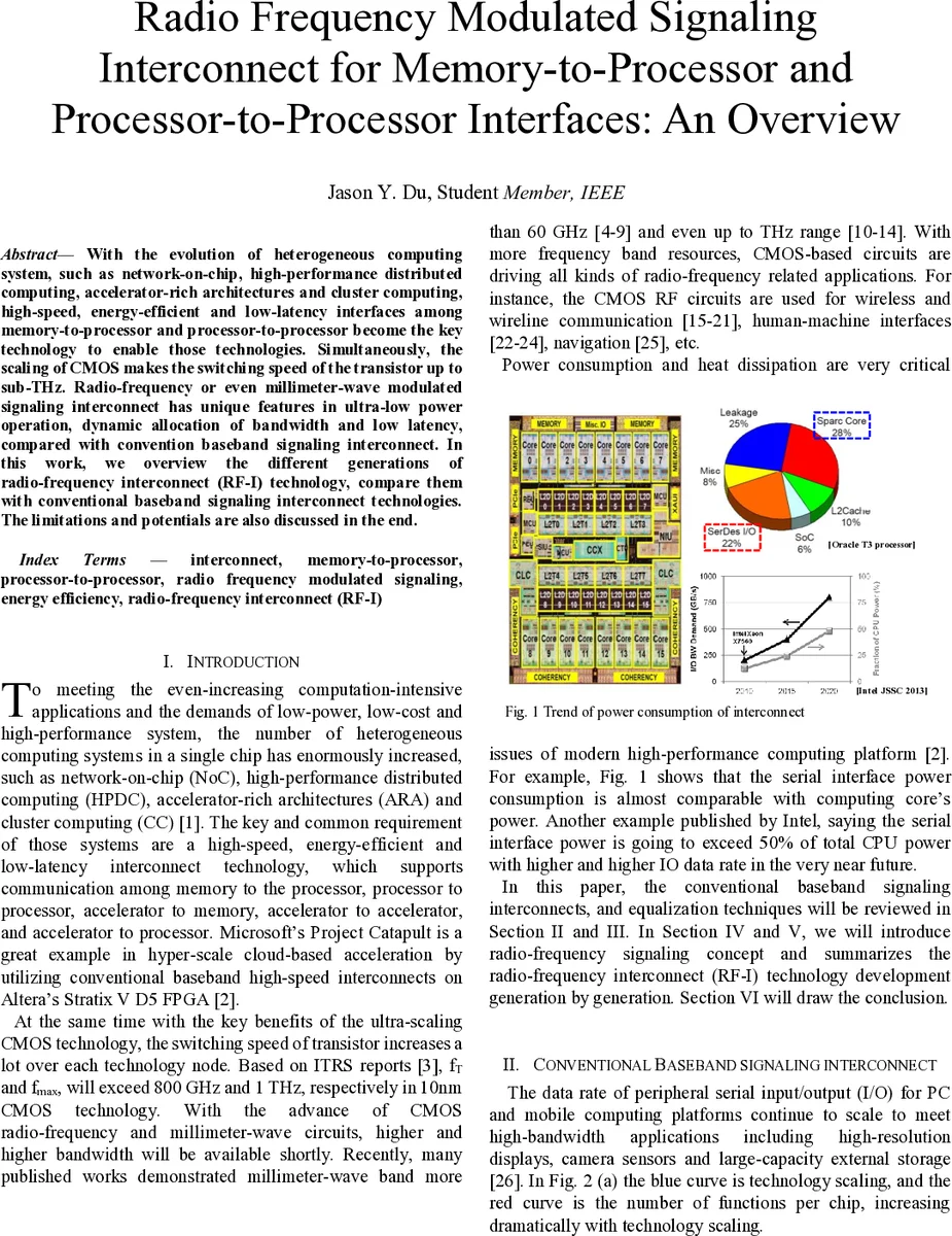
With the evolution of heterogeneous computing system, such as network-on-chip, high-performance distributed computing, accelerator-rich architectures and cluster computing, high-speed, energy-efficient and low-latency interfaces among memory-to-processor and processor-to-processor become the key technology to enable those technologies. Simultaneously, the scaling of CMOS makes the switching speed of the transistor up to sub-THz. Radio-frequency or even millimeter-wave modulated signaling interconnect has unique features in ultra-low power operation, dynamic allocation of bandwidth and low latency, compared with convention baseband signaling interconnect. In this work, we overview the different generations of radio-frequency interconnect (RF-I) technology, compare them with conventional baseband signaling interconnect technologies. The limitations and potentials are also discussed in the end.
💡 Research Summary
The paper surveys the emerging need for high‑speed, energy‑efficient, low‑latency interconnects between memory and processors as well as between processors in heterogeneous computing systems such as Network‑on‑Chip (NoC), high‑performance distributed computing (HPDC), accelerator‑rich architectures (ARA) and cluster computing. It points out that CMOS scaling has pushed transistor switching speeds into the sub‑THz regime (fT ≈ 800 GHz, fmax ≈ 1 THz in 10 nm), opening a frequency budget far beyond what conventional baseband serial links can exploit.
Section II reviews conventional baseband serial interconnects. Early designs (1980s) treated on‑chip wires and PCB traces as simple lumped capacitors; later generations (1990s‑2000s) required transmission‑line modeling, impedance matching, and equalization to combat ISI, reflections, and bandwidth limitations. Modern mobile and PC interfaces now exceed 10 Gb/s, but the non‑idealities of vias, bumps, package traces, connectors, and low‑cost cables force designers to combine FIR transmit‑side equalization, continuous‑time linear equalization (CTLE), and decision‑feedback equalization (DFE) on the receiver. This multi‑technique approach raises power consumption, design complexity, and sensitivity to process variations.
Section III details these equalization techniques, illustrating how a single‑bit pulse spreads into long tails that cause severe ISI at high data rates, and how the combination of FIR, CTLE, and DFE can mitigate the effect only at the cost of additional circuitry and energy.
Section IV introduces the concept of radio‑frequency modulated signaling (RF‑I). By allocating several orthogonal carrier frequencies (e.g., 3 GHz, 6 GHz, 10 GHz) and mapping different subsets of parallel data streams onto each carrier with modulation schemes such as PAM‑8, QPSK, 16‑QAM, or 256‑QAM, the system creates independent sub‑bands in the frequency domain. This multi‑band approach offers three key advantages: (1) it can avoid deep notches in the channel by selecting carriers that lie in transparent regions, (2) each sub‑band exhibits a self‑equalization effect that relaxes the need for aggressive analog equalization, and (3) total throughput scales linearly with the number of carriers and the order of modulation.
Section V surveys five generations of RF‑I transceivers reported between 2009 and 2016:
- 2009 VLSI (Tam) – 30‑50 GHz mm‑wave carriers, on‑chip 5 mm trace, 10 Gb/s aggregate, OOK, limited to point‑to‑point NoC links.
- 2012 ISSCC (Kim) – 18 GHz carrier, 5 cm FR‑4 PCB trace, 8 Gb/s, OOK, still point‑to‑point but with longer reach.
- 2015 CICC – Carrier frequencies reduced below 10 GHz, QPSK modulation, 4 Gb/s over 2‑inch copper traces, 2 pJ/bit energy.
- 2016 ISSCC – Dual carriers (3 GHz, 6 GHz) with 16‑QAM/PAM‑4, 10 Gb/s per differential pair, 1 pJ/bit, first demonstration of multi‑drop bus support.
- 2016 VLSI – “Cognitive” transmitter that sweeps a continuous wave to learn the channel response, then dynamically selects carrier(s), modulation order (up to 256‑QAM/PAM‑16), and bandwidth. Achieves 16 Gb/s per pair with <1 pJ/bit, works over low‑cost cables, connectors, and multi‑drop memory buses without any explicit equalization.
The table in the paper summarizes these generations, showing a clear trend: lowering carrier frequency to avoid mm‑wave losses, increasing modulation order to boost spectral efficiency, extending the physical channel, and dramatically improving energy per bit. The latest generation’s adaptive learning capability is highlighted as a breakthrough that can automatically compensate for process variations, connector tolerances, and deep frequency notches, thereby simplifying the PHY design.
Section VI concludes that RF‑I offers a fundamentally different trade‑off space compared with conventional baseband links: frequency‑domain multiplexing, reduced equalization burden, and sub‑picojoule energy per bit. However, the reported experiments are still limited to point‑to‑point or modest multi‑drop scenarios. The authors call for further research on scaling RF‑I to large‑scale NoC fabrics, reliability under temperature and voltage stress, and the development of industry‑wide standards.
Overall, the paper convincingly argues that the convergence of ultra‑fast CMOS RF circuits and sophisticated multi‑band modulation schemes can overcome the bandwidth, power, and latency bottlenecks of today’s serial interconnects, positioning RF‑I as a promising candidate for next‑generation memory‑processor and processor‑processor interfaces.
Comments & Academic Discussion
Loading comments...
Leave a Comment