Universal Quantum Circuits
We define and construct efficient depth-universal and almost-size-universal quantum circuits. Such circuits can be viewed as general-purpose simulators for central classes of quantum circuits and can be used to capture the computational power of the …
Authors: Debajyoti Bera, Stephen Fenner, Frederic Green
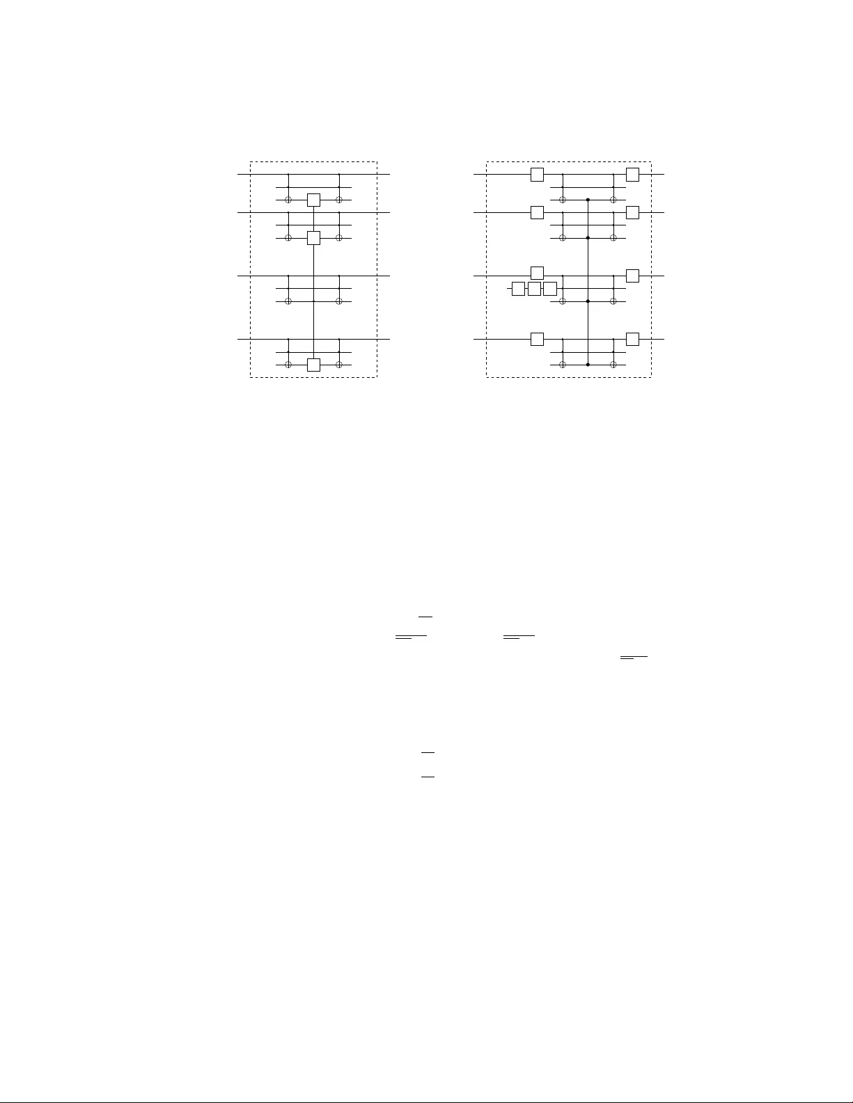
Univ ersal Quan tum Circuits Deba jy oti Bera 1 , Stephen F enner 2 , F rederic Green 3 , and Stev e Homer 1 1 Boston Univ ersity , Departmen t of Computer Science, Boston, MA 02134. ? 2 Univ ersity of South Carolina, Department of Computer Science and Engineering, Colum bia, SC 29208. ?? 3 Clark Universit y , Department of Mathematics and Computer Science, W orcester, MA 01610. ? ? ? Abstract. W e define and construct efficient depth-univ ersal and almost- size-univ ersal quan tum circuits. Suc h circuits can b e viewed as general- purp ose sim ulators for central classes of quantum circuits and can b e used to capture the computational pow er of the circuit class b eing simulated. F or depth we construct univ ersal circuits whose depth is the same order as the circuits b eing simulated. F or size, there is a log factor blow-up in the universal circuits constructed here. W e prov e that this construction is nearly optimal. 1 In tro duction Lik e resource-b ounded univ ersal T uring mac hines, efficien tly constructed univ er- sal circuits capture the hardness of languages computed b y circuits in a given circuit class. As a result, the study of the existence and complexity of univ er- sal circuits for quan tum circuit classes pro vides insight into the computational strength of suc h circuits, as w ell as their limits. There is b oth a theoretical and a practical asp ect to this study . The existence of a univ ersal circuit family for a complexity class defined by resource b ounds (depth, size, gate width, etc.) provides an upp er b ound on the resources needed to compute any circuit in that class. It also op ens up p ossibilities for proving lo wer b ounds on the hard languages in the class, as suc h bounds would follow from a lo wer b ound proof for the language computed b y a universal circuit family for the circuit class. More precisely , the sp ecific, efficien t construction of a universal circuit for a class of circuits yields, for a fixed input size, a single circuit whic h can b e used to carry out the computation of every circuit (with that same input size) in that family , basically a c hip or pro cessor for that class of circuits. The more efficient the construction of the universal circuit, the smaller the pro cessor for that class. ? { ( dbera | homer ) } @cs.bu.edu . Partially supp orted by the National Securit y Agency (NSA) and Adv anced Research and Developmen t Agency (ARDA) under Army Re- searc h Office (ARO) con tract num ber DAAD 19-02-1-0058. ?? fenner@cse.sc.edu . Partially supp orted b y NSF grant CCF-05-15269. ? ? ? fgreen@black.clarku.edu . P artially supp orted b y the NSA and ARD A under AR O con tract num b er DAAD 19-02-1-0058. F urthermore, the universal circuit is in a sense a compiler for all p ossible computations of all circuits in this family . It can b e used to efficiently program all p ossible computations capable of b eing carried out by circuits in this circuit class, and in doing so automatically acts as a general purpose simulator and with as little loss of efficiency as is p ossible. In the case of quantum circuits there are particular issues relating to the requiremen ts that computations must b e clean and reversible which come in to pla y , and to an extent complicate the classical methods. Still muc h of our mo- tiv ation for this w ork originates with classical results due to Co ok, V aliant, and others [CH85,V al76]. Co ok and Ho ov er considered depth univ ersality and de- scrib ed a depth-univ ersal uniform circuit family for circuits of depth Ω (log n ). V alian t studied size universalit y and show ed how to construct univ ersal circuits of size O ( s log s ) to simulate any circuit of size s . (See Section 1.1.) Definition 1 (Univ ersal Quan tum Circuits). Fix n > 0 and let C b e a collection of quantum circuits on n qubits. A quantum circuit U on n + m qubits is universal for C if, for ev ery circuit C ∈ C , there is a string x ∈ { 0 , 1 } m (the enc o ding ) such that for all strings y ∈ { 0 , 1 } n (the data ), U ( | y i ⊗ | x i ) = C | y i ⊗ | x i . The circuit collections w e are interested in are usually defined b y b ounding v arious parameters such as the size (num b er of gates), depth (n umber of la yers of gates acting sim ultaneously on disjoin t sets of qubits), or palette of allo w ed gates (e.g., Hadamard, π / 8, CNOT). As in the classical case, we also wan t our universal circuits to b e efficient in v arious wa ys. F or one, we restrict them to using the same gate family as the circuits they simulate. W e may also wan t to restrict their size or the num b er m of qubits they use for the enco ding. W e are particularly concerned with the depth of univ ersal circuits. Definition 2 (Depth-Univ ersal Quan tum Circuits). Fix a family F of uni- tary quan tum gates. A family of quantum circuits { U n,d } n,d> 0 is depth-universal over F if 1. U n,d is universal for n -qubit circuits with depth ≤ d using gates from F , 2. U n,d only uses gates drawn from F , 3. U n,d has depth O ( d ), and 4. the num b er of enco ding qubits of U n,d is p olynomial in n and d . Depth-univ ersal circuits are desirable b ecause they c an sim ulate any circuit within a constan t slo w-down factor. Thus they are as time-efficien t as p ossible. Our first result, presented in Section 3, shows that depth-universal quantum circuits exist for the gate families F = { H, T } ∪ { F n | n ≥ 1 } and F 0 = { H , T } ∪ { F n | n ≥ 1 } ∪ {∧ n ( X ) | n ≥ 1 } , where H and T are the Hadamard and π / 8 gates, resp ectively , and F n and ∧ n ( X ) are the ( n + 1)-qubit fanout and ( n + 1)- qubit T offoli gates, resp ectively (see Section 2). Theorem 3. Depth-universal quantum cir cuits exist over F and over F 0 . Such cir cuits use O ( n 2 d ) qubits and c an b e built lo g-sp ac e uniformly in n and d . Note that the results for the tw o circuit families are indep endent, because it is not known whether n -qubit T offoli gates can b e implemented exactly in constan t depth using single-qubit gates and fanout gates, although they can b e appro ximated this wa y [HS05]. It w ould b e nice to find depth-univ ersal circuits ov er families of b ounded- width gates 4 suc h as { H, T , CNOT } . Depth-universal circuits with b ounded- width gates, if they exist, must hav e depth Ω (log n ) and th us can only depth- efficien tly simulate circuits with depth Ω (log n ). This can be easily seen as fol- lo ws: Supp ose all you wan ted was a universal circuit U for depth-1 circuits on n qubits that use CNOT gates only . Since any pair of the n qubits could p otentially b e connected with a CNOT gate, that pair m ust b e connected somehow (indi- rectly p erhaps) within the circuit U . Th us any data input qubit can p otentially affect an y of the other n − 1 data output qubits. Since U only has constan t-width gates, the n um b er of qubits affected by any given data input increases b y only a constant factor p er lay er, and so U m ust ha ve Ω (log n ) lay ers. One can therefore only hop e to find depth-universal circuits for circuits of depth Ω (log n ) ov er bounded-width gates. Although such circuits exist in the classical case (see b elow), we are unable to construct them in the quantum case (see Section 6). 1.1 Other relev ant work The study of quantum circuit complexit y w as originated b y Y ao [Y ao]. The basic definitions and first results in this researc h area can be found in Nielsen and Chuang [NC00]. Most of the researc h on univ ersal quantum circuit classes deals with finding small, natural, universal sets of gates which can be used in quan tum circuits to efficien tly simulate an y quantum computation. Our problem and point of view here is quite differen t. W e hav e the goal of constructing, for a natural class C of quantum circuits, a single family of quantu m circuits which can efficien tly simulate all circuits on the class C . In this pap er we consider classes C which hav e significant resource b ounds (small or even constant depth, or fixed size) and ask that the corresp onding universal circuits family to hav e similar depth or size b ounds. Co ok and Ho ov er [CH85] considered the problem of constructing general- purp ose classical (Bo olean) circuits using gates with fanin t wo. They asked whether, given n, c, d , there is a circuit U of size c O (1) and depth O ( d ) that can sim ulate any n -input circuit of size c and depth d . Co ok and Hoov er con- structed a depth-universal circuit for depth Ω (log n ) and polynomial size, but whic h tak es as input a nonstandard encoding of the circuit, and they also pre- sen ted a circuit with depth O (log n log log n ) to con vert the standard enco ding of the circuit to the required enco ding. 4 The width of a gate is the num b er of qubits it acts up on. V alian t lo oked at a similar problem—trying to minimize the size of the uni- v ersal circuit [V al76]. He considered classical circuits built from fanin 2 gates (but with unbounded fanout) and em b edded the circuit in a larger universal graph. Using switches at key vertices of the universal graph, any graph (circuit) can be embedded in it. He managed to create univ ersal graphs for differen t t yp es of circuits and show ed how to construct a O ( c log c )-size and O ( c )-depth univer- sal circuit. He also show ed that his constructions ha ve size within a constant m ultiplicative factor of the information theoretic low er bound. F or quantum circuits, Nielsen and Chuang (in [NC97]) considered the prob- lem of building generic univ ersal circuits, or pr o gr ammable universal gate arr ays as they call them. Their universal circuits work on tw o quantum registers, a data register and a program register. They do not consider any size or depth b ound on the circuits and show that simulating ev ery p ossible unitary op eration requires completely orthogonal programs in the program register. Since there are infinitely man y possible unitary op erations, an y universal circuit w ould re- quire an infinite num b er of qubits in the program register. This sho ws that it is not p ossible to hav e a generic universal circuit whic h works for all circuits of a certain input length. Ho wev er they sho wed that it is p ossible to construct an extremely weak type of probabilistic univ ersal circuit with size linear in the n umber of inputs to the sim ulated circuit. Sousa and Ramos considered a similar problem of creating a universal quan- tum circuit to simulate any quantum gate [SR07]. They construct a basic build- ing blo ck whic h can b e used to implement an y single-qubit or CNOT gate on n qubits by switching certain gates on and off. They sho wed how to combine sev eral of these building blo cks to implement any n -qubit quantum gate. 1.2 Outline of the pap er F or the rest of the pap er, we will use U to denote the universal circuit and C to denote the circuit b eing sim ulated. W e define the quantum gates we will use in Section 2. The construction of depth-universal circuits is in Section 3. W e briefly describ e the construction of almost-size-universal quantum circuits in Section 4. W e mention a couple of miscellaneous results in Section 5. 2 Preliminaries W e assume the standard notions of quan tum states, quan tum circuits, and quan- tum gates describ ed in [NC00], in particular, H (Hadamard), T ( π / 8), S = T 2 (phase), and CNOT (controlled NOT). W e will also need some additional gates, whic h w e no w motiv ate. The depth-universal circuits we construct require the ability to feed the output of a single gate to many other gates. While this op eration, commonly kno wn as fanout, is common in classical circuits, cop ying an arbitrary quan- tum state unitarily is not p ossible in quantum circuits due to the no-cloning theorem [NC00]. It turns out that w e can construct our circuits using a classi- cal notion of fanout operation, defined as the fanout gate F n : | c, t 1 , . . . , t n i 7→ | c, c ⊕ t 1 , . . . , c ⊕ t n i for any of the standard basis states | c i (the con trol) and | t 1 i , . . . , | t n i (the targets) and extended linearly to other states 5 [FF GHZ06]. F n can b e constructed in depth lg n using CNOT gates. W e need to use unbounded fanout gates to achiev e full depth universalit y . W e also use the unb ounde d T of- foli gate ∧ n ( X ) : | c 1 , . . . , c n , t i 7→ | c 1 , . . . , c n , t ⊕ V n i =1 c i i . W e reserve the term “T offoli gate” to refer to the (standard) T offoli gate ∧ 2 ( X ), whic h is defined on three qubits. In addition to the fanout gate, our construction requires us to use con trolled v ersions of the gates used in the simulated circuit. F or most of the commonly used basis sets of gates (e.g., T off oli gate, Hadamard gate, and phase gate S ), the gates themselves are sufficient to construct their controlled versions (e.g., a con trolled Hadamard gate can b e constructed using a T offoli gate and Hadamard and phase gates). Depth or size universalit y requires that the controlled v ersions of the gates should b e constructible using the gates themselv es within proper depth or size, as required. Definition 4 (Closed under con trolled operation). A set of quantum gates G = { G 1 , . . . } is said to b e close d under c ontr ol le d op er ation if for eac h G i ∈ G , the con trolled version of the gate C- G i | c i| t i − → | c i G c i | t i can b e implemented in constan t depth and size using the gates in G . Here, | c i is a single qubit and G i could b e a single or a m ulti-qubit gate. Note that CNOT = F 1 , and given H , T , and CNOT we can implement the T offoli gate via a standard constan t-size circuit [NC00]. W e can implement the phase gate S as T 2 , and since T 8 = I , we can implement S † = T 6 and T † = T 7 . A gener alize d Z gate , which we will hereafter refer to simply as a Z gate , is an extension of the single-qubit Pauli Z gate ( | x i 7→ ( − 1) x | x i ) to multiple qubits: | x 1 , · · · , x n i Z 7→ ( − 1) x 1 x 2 ··· x n | x 1 , . . . , x n i . A Z gate can b e constructed easily (in constant depth and size) from a single un b ounded T offoli gate (and vice versa) by conjugating the target qubit of the un b ounded T offoli gate with H gates (i.e., placing H on b oth sides of the T offoli gate on its target qubit). Similarly , a Z -fanout gate Z n applies the single-qubit Z gate to each of n target qubits if the con trol qubit is set: | c, t 1 , · · · , t n i Z n 7→ ( − 1) c · ( t 1 + ··· + t n ) | c, t 1 , . . . , t n i . A Z n gate can b e constructed from a single F n gate and vice v ersa in constant depth (although not constant size) by conjugating each target with H gates. So, in our depth-universal circuit construction, we can use either or both of these types of gates. Similarly for unbounded T offoli versus Z gates. Z gates 5 This do es not con tradict the no-cloning theorem as only classical states are copied. and Z -fanout gates are important because they only change the phase, leaving the v alues of the qubits intact (they are represented by diagonal matrices in the computational basis). This allows us to use a trick due to Høyer and ˇ Spalek [HS05] and run all p ossible gates for a la yer in parallel. 3 Depth-univ ersal quan tum circuits In this section, w e prov e Theorem 3, i.e., that depth-universal circuits exist for eac h of the gate families F = { H, T } ∪ { F n | n ≥ 1 } , F 0 = { H , T } ∪ { F n | n ≥ 1 } ∪ {∧ n ( X ) | n ≥ 1 } . W e first giv e the pro of for F then show how to modify it for F 0 . The depth-universal circuit U we construct sim ulates the input circuit C lay er b y lay er, where a lay er consists of the collection of all its gates at a fixed depth. C is enco ded in a slightly altered form, ho wev er. First, all the fanout gates in C are replaced with Z -fanout gates on the same qubits with H gates conjugating the targets. At w orst, this may roughly double the depth of C (adjacent H gates cancel). Each lay er of the resulting circuit is then separated in to three adjacent la yers: the first ha ving only the H gates of the original lay er, the second only the T gates, and the third only the Z -fanout gates. U then simulates each lay er of the mo dified C b y a constant n umber of its o wn la yers. W e describ e next ho w these lay ers are constructed. Simulating single-qubit gates. The circuit to simulate an n -qubit lay er of single- qubit gates of type G , say , consists of a lay er of controlled- G gates where the con trol qubits are fed from the encoding and the target qubits are the data qubits. Figure 1 sho ws a la yer of G gates, where G ∈ { H , T } , con trolled using H , S , T , CNOT, and T offoli gates. T o simulate G gates on qubits i 1 , . . . , i k , sa y , set c i 1 , . . . , c i k to 1 and the rest of the c -qubits to 0. d n d 1 c n c 1 d 2 = | 0 i = c 2 . . . where G ∈ { H , T } and G S † T † S T G H T T H H G Fig. 1. Simulating a lay er of single-qubit G gates with controlled G gates. The ancilla in the implementation of the controlled T gate is assumed part of the enco ding. The ancilla is reset to 0 at the end and hence can b e reused for implementing all T lay ers. Simulating Z -fanout gates. The circuit to simulate a Z -fanout la yer is sho wn in Figure 2. The top n qubits are the original data qubits. The rest are ancilla . . . . . . . . . . . . . . . . . . . . . . . . . . . . . . . . . . . . . . . . . . . . . . . . . . . B n B 1 B 2 B 3 d 1 d n . . . . . . 0 0 . . . 0 0 . . . 0 0 . . . A 1 A 2 A 3 A n Fig. 2. Simulating a lay er of Z -fanout gates. qubits. All the qubits are arranged in n blo cks B 1 , . . . , B n of n qubits p er blo ck. The qubits in blo ck B i are lab eled b i 1 , . . . , b in . Eac h A i sub circuit lo oks lik e Figure 3. The qubits c i 1 , . . . , c in are enco ding qubits. The large gate b etw een the t wo columns of T offoli gates is a Z -fanout gate with its control on the i th ancilla (corresp onding to b ii and c ii ) and targets on all the other ancillæ. Here is the state ev olution from | d i = | d 1 · · · d n i , suppressing the c ij qubits and ancillæ internal to the A i sub circuits in the ket labels. Note that after the first lay er of fanouts, each qubit b ij carries the v alue d j . | d , 0 , . . . , 0 i 7→ | d , d , . . . , d i 7→ ( − 1) P i d i c ii ( P j 6 = i d j c ij ) | d , d , . . . , d i 7→ ( − 1) P i d i c ii ( P j 6 = i d j c ij ) | d , 0 , . . . , 0 i . T o sim ulate some Z -fanout gate G of C whose con trol is on the i th qubit, sa y , we do this in blo ck B i b y setting c ii to 1 and setting c ij to 1 for every j where the j th qubit is a target of G . All the other c -qubits in B i are set to 0. W e can do this in separate blo cks for multiple Z -fanout gates on the same lay er, b ecause no tw o gates can share the same control qubit. Any c -qubits in unused blo c ks are set to 0. b in b i 2 b ii c i 1 0 c i 2 0 c ii 0 c in 0 . . . . . . . . . . . . . . . . . . . . . . . . b i 1 Z Z Z Fig. 3. Sub circuit A i in the simulation of Z -fanout gates. c ii . . . . . . . . . . . . . . . b i 1 b i 2 b ii b in 1 c i 1 1 c i 2 1 c in 1 . . . . . . . . . X Z X X X X X X X X X Fig. 4. Sub circuit A i for a la yer of Z gates. Simulating unb ounde d T offoli gates. W e can mo dify the construction ab ov e to accommo date unbounded T offoli gates (gate family F 0 ), or equiv alen tly Z gates, b y breaking eac h lay er of C in to four adjacent lay ers, the first three b eing as b efore, and the fourth containing only Z gates. The top-lev el circuit to simulate a lay er of Z gates lo oks just as b efore (Figure 2), except now each A i sub circuit lo oks a bit different and is shown in Figure 4, where the central gate is a Z gate connecting the ancillæ. As before, the qubits c i 1 , . . . , c in are encoding qubits. The X Z X gates on c ii m ultiply the ov erall phase by ( − 1) c i i . When the Z gate of A i is applied, its j th contact p oint is in the state b ij c ij . Note that b ij c ij = b ij if c ij = 1 and 1 otherwise. The Z gate then multiplies the ov erall phase by ( − 1) Q j ( b ij c ij ) = ( − 1) Q j : c ij =1 b ij . The state thus evolv es as giv en below: | d , 0 , . . . , 0 i 7→ | d , d , . . . , d i 7→ ( − 1) P i c ii + Q j : c ij =1 b ij | d , d , . . . , d i 7→ ( − 1) P i c ii + Q j : c ij =1 b ij | d , 0 , . . . , 0 i T o sim ulate some Z gate G of C whose first qubit is i , say , we do this in block B i b y setting c ii to 1 and setting c ij to 1 for every j where the j th qubit is part of G . All the other c -qubits in B i are set to 0. As b efore, we can do this in separate blo cks for multiple gates on the same la yer, because no t wo gates can share the same first qubit. Any c -qubits in unused blo cks are set to 0, and it is easy to c heck that this makes the blo ck hav e no net effect. 4 Size-univ ersal quan tum circuits Similar to a depth-universal circuit, a size-universal cir cuit is a universal cir- cuit with the same order of the n um b er of gates as the circuit it is simulating. F ormally , Definition 5. A family { U n,c } of universal circuits for n -qubit circuits of size ≤ c is size-universal if SIZE( U n,c ) = O ( c ). A simple counting argument shows that it is not possible to obtain a com- pletely size-universal circuit for fanin-2 circuits. Consider all circuits with c fanin- 2 gates where one input of eac h gate is the first qubit. There are ( n − 1) c p ossible circuits. Then consider similar circuits where there is no gate with input as the first qubit and contin ue recursively . Thus the num b er of p ossible fanin-2 circuits is Ω (( n − 1) c +1 ). Since all the enco ding bits hav e to b e connected to some of the fanin-2 gates in the univ ersal circuit, it m ust ha ve Ω ( c log n ) gates. W e use V aliant’s idea of universal graphs [V al76] to construct a univ ersal family of fanin-2 circuits that are very close to the afforemen tioned low er b ound. As b efore, we w ould like to simulate C b y using the same set of gates used in C . Our construction w orks for an y circuit using unbounded T offoli gates and an y set of single-qubit and 2-qubit gates closed under the controlled op eration. First we will define a universal directe d acyclic graph with n sp ecial vertices (called p oles ) in which w e can em bed an y circuit with n gates (considering the inputs also as gates). The embedding will map the wires in the circuit to paths in the graph. Definition 6 (Edge-em b edding [V al76]). An e dge-emb e dding ρ of G = ( V , E ) in to G 0 = ( V 0 , E 0 ) maps V one-to-one to V 0 and maps each edge ( i, j ) ∈ E to a directed path ρ ( i ) ρ ( j ) in G 0 suc h that distinct edges are mapp ed to edge- disjoin t paths. The graph of an y circuit of size n can b e represen ted as a directed acyclic graph with vertices { 1 , . . . , n } suc h that there is no edge from j to i for i < j and each vertex has fanin and fanout 2. Let Γ 2 ( n ) b e the set of all suc h graphs. Definition 7 (Edge-univ ersal graph [V al76]). A graph G 0 is e dge-universal for Γ 2 ( n ) if it has distinct poles p 1 , . . . , p n suc h that an y graph G ∈ Γ 2 ( n ) can b e edge-embedded into G 0 where each vertex i ∈ G is mapp ed to vertex ρ ( i ) = p i ∈ G 0 . Then, V aliant shows how to construct a universal graph. Theorem 8 ([V al76]). Ther e is a c onstant k such that for al l n ther e exists an acyclic gr aph G 0 that is e dge-universal for Γ 2 ( n ) , and G 0 has k n lg n vertic es, e ach vertex having fanin and fanout 2 . It is fairly easy to construct a universal circuit using the universal graph. In fact, the universal circuit for circuits with n inputs and c gates will be an y edge-univ ersal graph for Γ 2 ( n + c ). Consider an y suc h edge-univ ersal graph G 0 . Then G 0 has c 0 = k ( n + c ) log ( n + c ) vertices for some k . These c 0 v ertices include fixed p oles p 1 , . . . , p n , p n +1 , . . . , p n + c and non-p ole v ertices. Create a quan tum circuit C 0 with c 0 gates (including the inputs and outputs) where G 0 describ es ho w the gates connect to eac h other. F or eac h of the vertices p 1 , . . . , p n of G 0 , remov e their incoming edges and replace the vertices by the input as sho wn in Figure 5. Replace each of the vertices p n +1 , . . . , p n + c with a sub circuit that applies an y of the single- or 2-qubit gates on the inputs, where the gate to apply is con trolled by the enco ding. E.g., Fig- ure 7 shows the gates at a p ole v ertex in a univ ersal circuit simulating CNOT and H gates. F or a non-p ole vertex, replace it with a subcircuit that swaps the incoming and outgoing wires (i.e., first input is connected to second output and second input is connected to first output) or directly connects them (i.e., first input is connected to first output and similarly for the second input). Again, the sub circuit is controlled by the enco ding which controls whether to sw ap or directly connect (see Figure 6). The edge disjoin tness prop erty guarantees that wires in the embedded circuit are mapp ed to paths in C 0 whic h can share a v ertex but cannot share any edge. ≡ g ate ( v out 1 ) g ate ( v out 2 ) x i 0 v out 2 v out 1 p i v in 1 v in 2 Fig. 5. The gate for a p ole vertex p i is mapp ed to input x i . c v Fig. 6. The gates at a non-p ole vertex v . The enco ding bit c v sp ecifies if first output qubit should b e mapp ed to first input or second input qubit and simi- larly for second output qubit. c d v c g v H Fig. 7. Example of the gates at a p ole vertex v sim ulating a circuit with CNOT and H gates. The encoding bits c g v sp ecify whic h kind of gate is at v ertex v , and the c d v sp ecify whic h qubit the gate acts on (for H gate) or whic h is the control qubit (for CNOT gate). T o simulate an y fanin-2 circuit C with c gates acting on n qubits, construct the edge-universal graph G 0 for Γ 2 ( n + c ). Em b ed the graph of C in to G 0 suc h that the input nodes of C are mapp ed to the p oles p 1 , . . . , p n in G 0 . No w for eac h gate of the circuit, consider the p ole to whic h it was mapp ed. Set a bit in the enco ding to denote the t yp e of the gate at that pole. F or the non-p ole vertices, set a bit in the enco ding to specify whether the t w o input v alues should be sw app ed or mapp ed directly to the tw o output v alues. The size of the enco ding is ( n + c )(log | gates | + 1) + ( | Γ 2 ( n + c ) | − ( n + c )) whic h is O ( c log c ) for polynomial- size circuits. This construction gives us a universal circuit with a logarithmic blo w-up in size. Theorem 9. Ther e is a c onstant k and a family of universal cir cuits U n,c that c an simulate every cir cuit with c gates acting on n qubits such that SIZE ( U n,c ) = k ( n + c ) log ( n + c ) . W e can use a similar idea for circuits with unbounded fanin. First we decom- p ose the unbounded fanin gates using b ounded fanin gates (fanin 2 in this case). This is doable for most of the common un b ounded fanin gates. F or example, an un b ounded T offoli gate of size f can b e constructed using Θ ( f ) successive T offoli gates of size 3, which can in turn b e implemented using Hadamard, phase, π / 8 and CNOT gates [NC00]. So any circuit of size c consisting of Hadamard, π/ 8 and unbounded T offoli gates can b e transformed in to an equiv alent circuit with size at most O ( cn ) consisting of these single-qubit gates and CNOT gates. The rest of the construction follo ws as b efore. Corollary 1. Ther e is a family of universal cir cuits U n,c that c an simulate quantum cir cuits of size c on n qubits and c onsisting of Hadamar d, π / 8 , and unb ounde d T offoli gates such that SIZE ( U n,c ) = O ( nc log( nc )) . 5 Other results Cir cuit enc o ding. W e hav e b een mostly concerned with the actual simulation of a quantu m circuit C by the univ ersal circuit U . It is p ossible, how ever, to hide some complexity of the simulation in U ’s description of C itself. Usually , the description of a classical circuit describes the underlying graph of the circuit and sp ecifies the gates at eac h v ertex. W e can similarly describe a quan tum circuit b y its graph structure. The description is extremely compact with size prop ortional to the size of the circuit. How ev er, we use a description that is more natural for quan tum circuits and esp ecially suitable for sim ulation. The description stores the grid structure of the circuit; the ro ws of the grid correspond to the qubits, and the columns corresp ond to the differen t la yers of the circuit. This description is not unique for an y given circuit and its size is O ( nd ), where n is the num b er of qubits and d is the depth of the circuit. A graph-based description can be easily conv erted to this grid-based description in p olynomial time. Depth-universal classic al cir cuits. The tec hniques of Section 3 can b e easily adapted to build depth-universal circuits for a v ariet y of classical (Boolean) circuit classes with unbounded gates, e.g., AC, ACC, and TC circuits. The k ey reason is that these big gates are all “self-similar” in the sense that fixing some of the inputs can yield a smaller gate of the same t yp e. W e will present these results in the full pap er. 6 Op en Problems A num b er of natural, interesting op en problems remain. F anout gates are used in our construction of a depth-universal circuit family . Is the fanout gate necessary in our construction? W e believe it is. In fact, we do not know how to simulate depth- d circuits ov er { H , T , CNOT } universally in depth O ( d ) without using fanout gates, even assuming that the circuits b eing sim ulated hav e depth Ω (log n ). The shallow est universal circuits with b ounded- width gates w e kno w of hav e a lg n blow-up factor in the depth, just b y replacing the fanout gates with log-depth circuits of CNOT gates. Our results apply to circuits with v ery sp ecific gate sets. Ho w m uc h can these gate sets b e generalized? Are similar results p ossible for any countable set of gates con taining Hadamard, unbounded T offoli, and fanout gates? W e show ed how to contruct a universal circuit with a logarithmic blo w-up in size. The construction is within a constant factor of the minim um p ossible size for p olynomial-size, b ounded-fanin circuits. How ever for constant-size circuits, w e b eliev e the low er b ound can b e tightened to match the prov en upp er b ound. F or un b ounded-fanin circuits, we construct a univ ersal circuit with size O ( nc log nc ) whic h is significantly larger than the b ounded fanin low er bound of Ω ( c log n ). W e think that a b etter low er b ound is p ossible for the unbounded-fanin case. Ac kno wledgments W e thank Mic hele Mosca and Debbie Leung for insightful discussions. The second author is grateful to Richard Cleve and IQC (W aterlo o) and to Harry Buhrman and CWI (Amsterdam) for their hospitality . References [BGH07] D. Bera, F. Green and S. Homer. Small depth quan tum circuits. SIGACT News , 38(2):35–50, 2007. [CH85] Stephen A. Cook and H. James Ho ov er. A depth-universal circuit. SIAM Journal on Computing , 14(4):833–839, 1985. [FF GHZ06] M. F ang, S. F enner, F. Green, S. Homer and Y. Zhang. Quantum low er b ounds for fanout. Quantum Information and Computation , 6(1):046– 057, 2006. [HS05] P . Høyer and R. ˇ Spalek. Quantum circuits with un b ounded fan-out. The- ory of Computing , 1:81–103, 2005. [NC97] M. A. Nielsen and I. L. Chuang. Programmable quantum gate arrays. Phys. R ev. Lett. , 79(2):321-324, 1997. [NC00] M. A. Nielsen and I. L. Ch uang. Quantum Computation and Quantum Information . Cambridge Universit y Press, 2000. [SR07] P . B. M. Sousa and R. V. Ramos. Univ ersal quantum circuit for n -qubit quan tum gate: A programmable quan tum gate. Quantum Information and Computation , 7(3):228–242, 2007. [V al76] Leslie G. V aliant. Univ ersal circuits (preliminary rep ort). In Pr o c e e dings of the 8th ACM Symposium on the The ory of Computing , 196–203, 1976. [Y ao] A. C.-C. Y ao. Quan tum circuit complexit y . In Pr o c e e dings of the 34th IEEE Symp osium on F oundations of Computer Science , 352–361, 1993.
Original Paper
Loading high-quality paper...
Comments & Academic Discussion
Loading comments...
Leave a Comment